
A Brief Look at Apple’s M2 Pro iGPU

Integrated GPUs are often low-end affairs. Even when graphics performance matters, a combination of cost, die space, memory bandwidth, and power constraints prevent iGPUs’ performance from reaching into mid-range discrete GPUs’ territory. But every rule has exceptions. Consoles like Xbox Series X and PlayStation 5 use large integrated GPUs, saving board space with a smaller footprint. Apple has been going all-in on iGPUs since they transitioned to in-house chips, so M2 Pro is another example of large iGPUs.
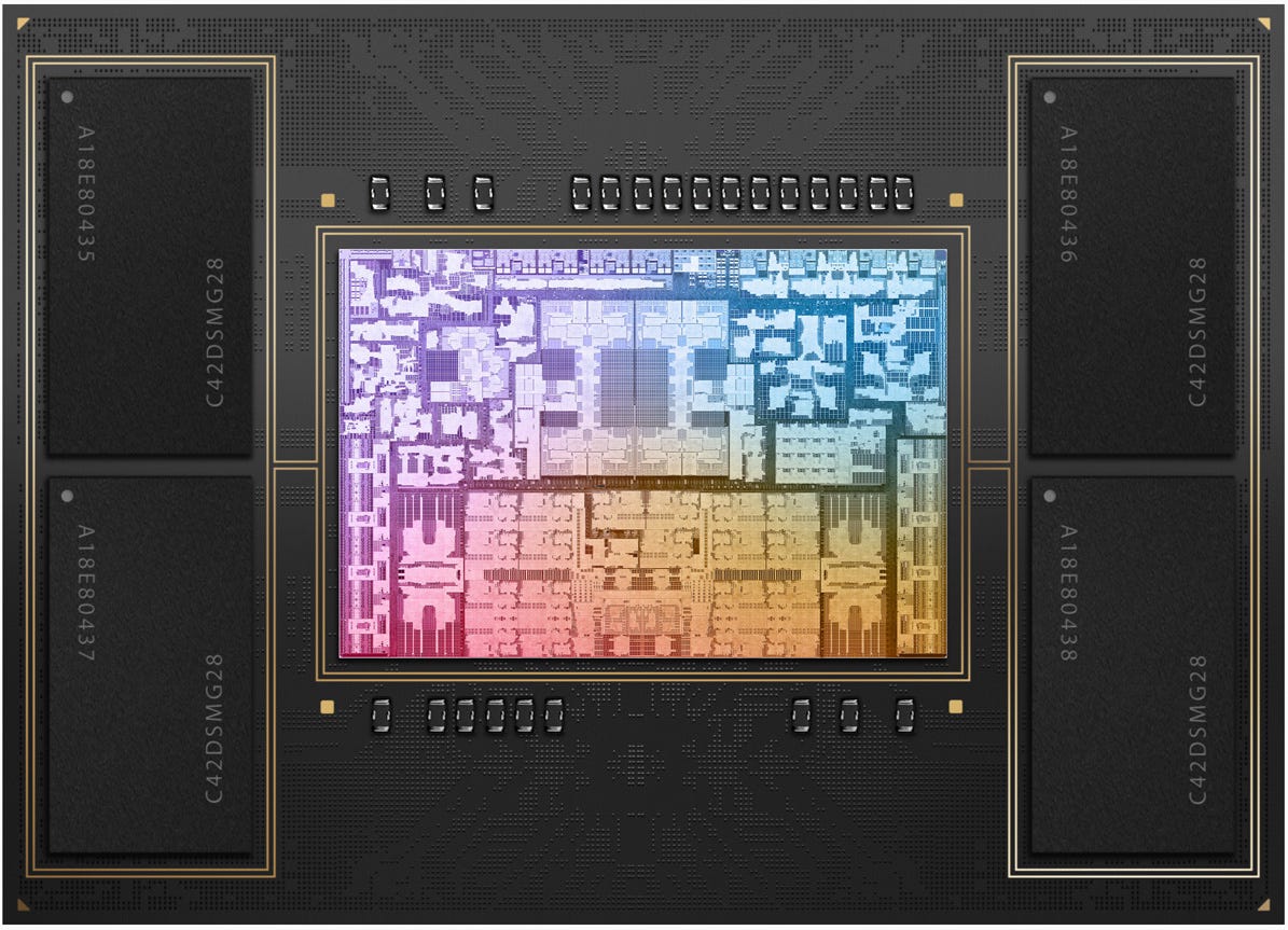
M2 Pro uses a ~289 mm2 die1, making it substantially larger than AMD Phoenix’s 178 mm2 die. Apple uses this massive amount of silicon to implement a 19 core iGPU. AWS is now offering M2 Pro instances, which allows us for some limited testing. In particular, the iGPU is accessible. Special thanks goes out to Titanic for renting a M2 Pro bare metal instance.
Cache and DRAM Latency
M2 Pro’s iGPU uses a traditional two-level cache hierarchy to accelerate GPU-side memory access. Like the M1, M2 Pro’s iGPU cache hierarchy starts with a tiny 8 KB L1 cache. It’s about as fast as the 32 KB L1 vector cache on Phoenix. Then, a 3 MB L2 cache provides ample capacity. Despite being 50% larger than Phoenix’s 2 MB L2, Apple achieves similar latency. Comparing to M1, M2 Pro’s larger iGPU roughly triples L2 caching capacity in exchange for a slight latency increase.
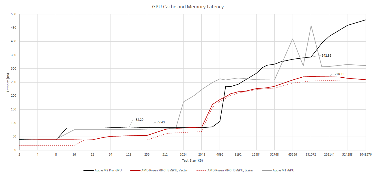
After spilling out of the L2 cache, M2 Pro’s iGPU accesses a system-level cache with a 234 ns latency. DRAM access takes more than 342 ns at the 128 MB test size. Going further sends latency beyond 400 ns, perhaps due to TLB misses. M2 Pro thus has higher DRAM access latency than AMD’s Phoenix, which has similar memory access latency to recent discrete GPUs.

M2 Pro’s DRAM latency is most similar to that of older Intel iGPUs. The i5-6600K’s HD 530 takes 312 ns to get data from DRAM with a 128 MB test array, which puts it just under the M2 Pro’s 342 ns.
OpenCL’s image1d_buffer_t gives access to a different first-level cache with 24 KB capacity. M2 Pro likely has a separate 24 KB texture cache. Accesses to this cache experience similar latency to those on NVIDIA’s Maxwell architecture.

Compute applications that can use buffer or texture accesses can get more first level caching capacity, but the 8 KB L1 data cache is disappointingly small. We haven’t seen GPU first level caches with this little capacity since AMD’s Terascale architecture from before 2011. Besides compute applications, games increasingly use compute shaders even when raytracing is not in the picture. At larger L1 cache would help keep bandwidth off the L2, reducing power consumption and improving performance.
Bandwidth
M2 Pro’s L2 is no slouch. The iGPU can pull over 1 TB/s from L2, putting it ahead of some older discrete GPUs like Radeon R9 390. A big iGPU demands more shared cache bandwidth, and M2 Pro is no exception.
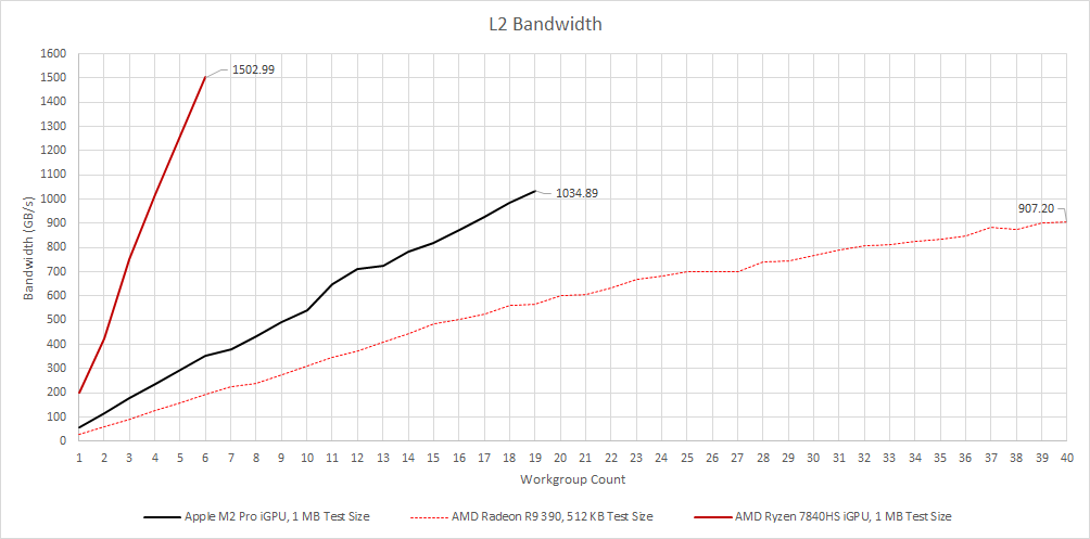
However, AMD’s Phoenix has a large L2 bandwidth lead. AMD has emphasized high bandwidth with RDNA 2 and RDNA 3, and sometimes it pays off (as we saw in Starfield). With small L1 caches, M2 Pro may be more reliant on L2 bandwidth than RDNA 3 or Nvidia’s Ada architecture.
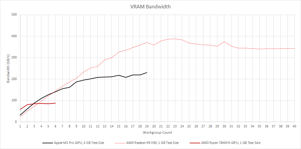
For access that spills out of cache, the situation flips around. Radeon R9 390 now comes out on top, thanks to its massive 512-bit GDDR5 memory bus. M2 Pro is still no joke and achieves over 200 GB/s of memory bandwidth thanks to its 256-bit LPDDR5 setup. AMD’s Phoenix uses a 128-bit memory bus and can’t get anywhere close.
Apple’s recently announced M3 Pro carries forward M2 Pro’s design goals, but memory bandwidth has been reduced to 150 GB/s. The M3 Pro can be configured with 18 GB or 36 GB of DRAM, compared to 16 or 32 GB on the M2 Pro. That divisible-by-3 number suggests Apple has switched to a 192-bit memory bus. In the discrete GPU world, the RX 6500 XT has just under 150 GB/s of bandwidth and slightly less FP32 throughput than the M2 Pro’s iGPU. M2 Pro’s very high DRAM bandwidth likely wasn’t helping most applications. A narrower, better utilized DRAM bus could save packaging and power costs.
Like Van Gogh and console chips, M2 Pro’s large memory bus aims to feed the GPU. Achieving the same 200 GB/s figure from the CPU side is not possible, but the CPU still benefits from it.

125 GB/s is a lot of bandwidth for eight cores, and is out of reach for desktop platforms. Just as Digital Foundry saw on console chips, M2 Pro’s memory latency is also higher but not to the same extent. M2 Pro’s CPU sees a 116.5 ns latency with a 1 GB test size using macOS’s default 16 KB page size.
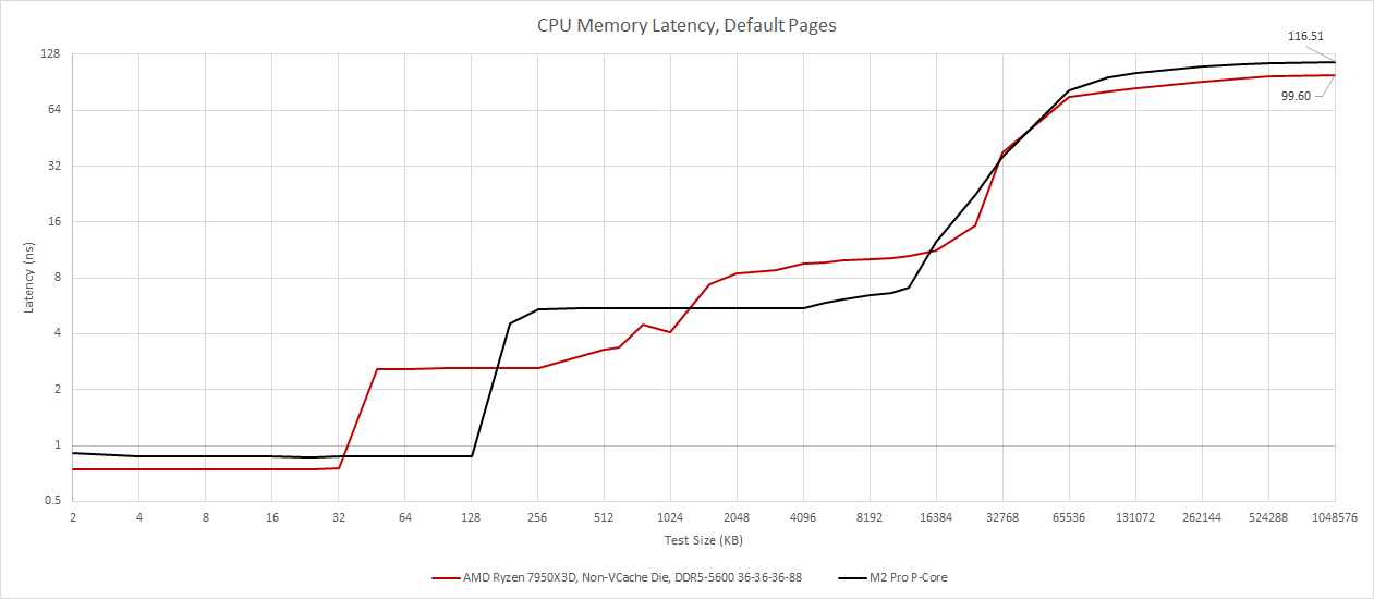
For comparison, AMD’s 7950X gets 84.06 ns using 4 KB pages over a 1 GB array. AMD’s Phoenix suffers from higher latency and hits 126.7 ns with the same 1 GB test size.
Local Memory Latency
GPU programs can allocate fast scratchpad memory, referred to local memory in OpenCL. M2 Pro allows a program to allocate up to 32 KB of local memory. Each GPU core could have more scratchpad storage though. For example, GCN has the same 32 KB limit, but each compute unit has 64 KB of scratchpad storage.
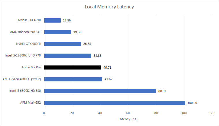
Local memory is directly addressed and therefore is usually faster than cache access, because tag comparisons aren’t needed. However, M2 Pro’s local memory takes slightly longer to access than the 8 KB L1 data cache. Recent discrete GPUs from AMD and NVIDIA enjoy faster access to their local memory.
Atomics
Curiously, using atomics on local memory is faster than pointer chasing with one thread. Atomics are used to ensure a complex operation on a value in memory to execute without interference, even if other threads are contending for access, which makes them useful for cross-thread communication. Here, we’re using OpenCL’s atomic_cmpxchg to pass a value between two threads through local memory.

Apple performs very well here and pulls ahead of GTX 980 Ti, even though M2 Pro’s local memory was slower for pointer chasing accesses. It’s still not as fast as recent discrete GPUs though.
We can also test atomics on global memory. These accesses are comparable to core-to-core latency tests on a CPU, and are harder to cope with because the two threads can be located anywhere on the GPU.
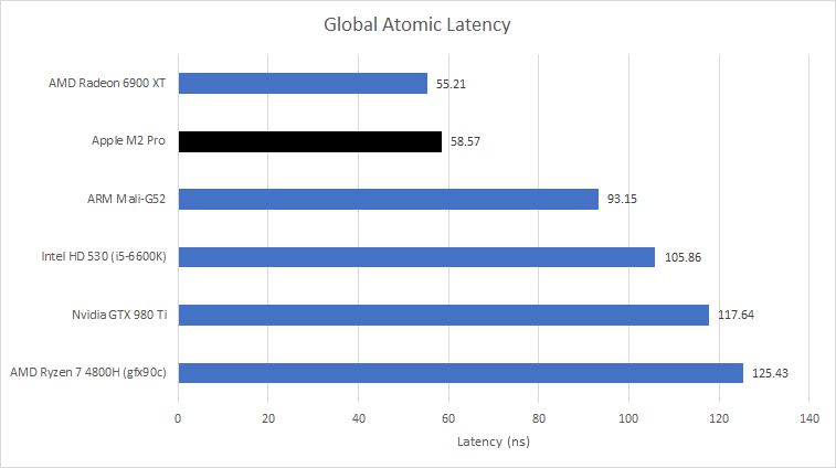
M2 Pro’s iGPU handles this well with 58.57 ns latency. It’s comparable to AMD’s RDNA 2, and much faster than older iGPUs from Intel and AMD.
FluidX3D
FluidX3D uses the lattice Boltzmann method (LBM) to simulate fluid behavior. It features special optimizations that let it use FP32 and still deliver accurate results in “all but extreme edge cases”. LBM isn’t cache friendly, so memory bandwidth has a large influence on FluidX3D results.
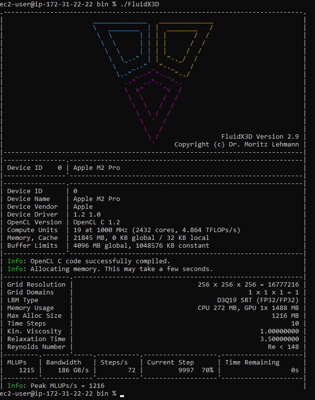
Here, M2 Pro’s iGPU sees a massive advantage over AMD’s Phoenix. From vkpeak, M2 Pro delivers 6.5 TFLOPs of FP32 performance. That puts it just under AMD’s Phoenix, though RDNA 3 achieves its 8.6 TFLOPs theoretical figure through a difficult-to-feed dual issue mechanism. In any case, there’s no arguing with a giant memory bus.
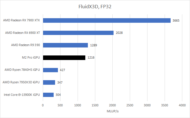
M2 Pro performs very closely to the old Radeon R9 390, which also has a massive memory bus. Recent discrete GPUs score higher because they have higher bandwidth GDDR6 setups. But M2 Pro stands in a class of its own if we focus on iGPUs.
Final Words
Large iGPUs have not taken off in the PC space. Consumers want to make their CPU and GPU choices separately. The CPU side demands high DRAM capacity but isn’t very sensitive to bandwidth. In contrast, the GPU side needs hundreds of gigabytes per second of DRAM bandwidth. Discrete GPUs separate these two pools, allowing the CPU and GPU to use the most appropriate memory technology. Finally, separate heat sinks allow more total cooling capacity, which is important for very large GPUs.
However, consoles have given big iGPUs a niche. Compact form factor and power efficiency take priority in consoles. Bringing the GPU on-die eliminates the need for PCIe interfaces and traces on the motherboard. CPU-to-GPU communication can be of higher bandwidth and more efficient with a monolithic die. A shared memory controller is more power efficient than two separate memory controllers with less area too. And it works well when the CPU-side memory demands are a rounding error compared to the GPU’s.
Apple has decided the same advantages justify the sacrifices. M2 Pro gets a very scaled up version of M1’s iGPU. L2 cache grows to 3 MB, and bandwidth increases from just under 400 GB/s on M1 to over 1 TB/s on M2 Pro. But even a larger L2 doesn’t provide enough memory bandwidth with a typical 128-bit memory bus setup. So Apple uses a 256-bit memory bus, making M2 Pro a console-like chip with over 200 GB/s of memory bandwidth on tap. But unlike console chips, M2 Pro gets its high bandwidth with minimal latency penalties. It’s an excellent compromise that lets M2 Pro compete with setups with separate CPUs and GPUs, irregardless whether a workload stresses the CPU or GPU.
But the limitations remain. M2 Pro can’t be configured with more than 32 GB of memory. Desktop DDR5 systems can pack 128 GB of DRAM. On-package memory and a huge chunk of leading-edge silicon also drive up costs. A Mac Mini with 32 GB of memory and a fully enabled M2 Pro costs $1999.

On that note, I’m skeptical of AMD Strix Halo rumors. Strix Halo is expected to combine 12 to 16 Zen 5 cores with up to 20 “RDNA 3.5” cores, and feed the whole thing with a 256-bit LPDDR5X memory controller. It feels like M2 Pro. But AMD caters to a different market. PC enthusiasts tend to value low cost and flexibility. A $1999 price tag to save every bit of power and area is a stretch when more powerful systems can be built for less. I doubt AMD can make Strix Halo cheaper either. M2 Pro looks costly not because of the Apple tax, but rather because giant monolithic dies on cutting edge nodes are expensive. With stiff competition from more flexible and cost effective options, and without a captive audience, Strix Halo is unlikely to enjoy the economy of scale that M2 Pro or console chips do.
M2 Pro’s large integrated GPU is therefore something few others besides Apple can pull off. It matches their goal of maximizing GPU and CPU power in a small form factor, and Apple has done a good job of making it work. It’ll be interesting to see what Apple pulls off with their next generation.
If you like our articles and journalism, and you want to support us in our endeavors, then consider heading over to our Patreon or our PayPal if you want to toss a few bucks our way. If you would like to talk with the Chips and Cheese staff and the people behind the scenes, then consider joining our Discord.
Appendix
According to Locuza and SemiAnalysis, the M2 P-Core is around 2.76 mm2. Pixel counting on Apple’s render gives a die size of about 289.22 mm2 if that’s accurate.