
Hot Chips 2023: AMD’s Phoenix SoC

AMD’s mobile and small form factor journey has been arduous. In the early 2010s, the company’s Bulldozer-derived CPU cores stood no chance as Intel made massive gains in power efficiency. Zen narrowed the gap, but AMD still had a lot of work to do. Idle power consumption was still worse than Intel’s. The GPU side was stronger thanks to AMD’s acquisition of ATI, but AMD’s integrated GPUs were often left using horribly out of date graphics architectures. Terascale 3 remained in use on APUs well after GCN discrete GPUs hit the market. AMD launched the Ryzen 7 5800H in 2021 with Vega (improved GCN) graphics, when desktop GPUs had already transitioned to using RDNA 2.
Recent AMD products have been turning the situation around. Van Gogh (Steam Deck APU) and Rembrandt finally brought RDNA 2 into integrated GPUs. Phoenix takes another step in the right direction, combining current-generation Zen 4 cores and RDNA 3 graphics into a potent package. We’d like to thank AMD for putting together an excellent Hot Chips presentation on the Phoenix SoC.

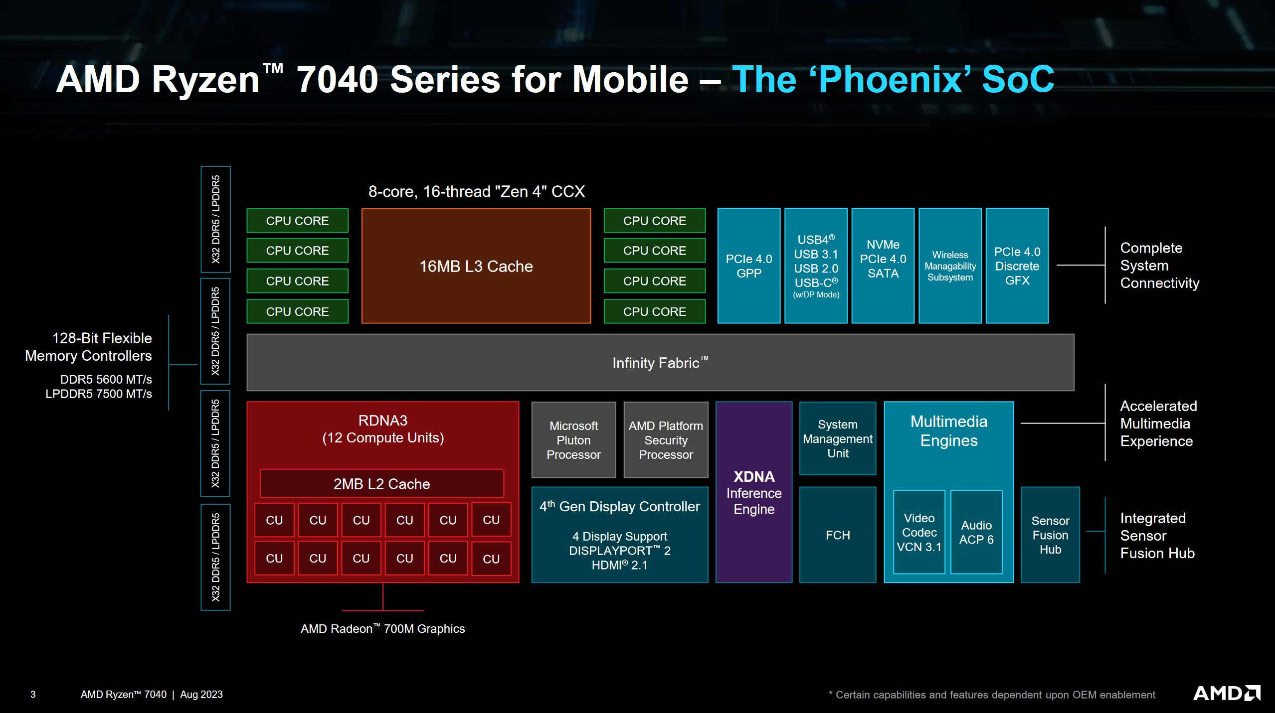
Alongside using up-to-date architectures for the all-important CPU and GPU, Phoenix integrates a variety of accelerators to improve power efficiency in specific applications. Intel had been integrating accelerators like their GNA AI accelerator for a while, and AMD is looking to catch up. An XDNA accelerator helps with machine learning inference, and an audio controller offloads signal processing from the CPU. Importantly for a mobile SoC, Phoenix also features a capable video engine.
We’re going to complement our coverage of AMD’s Phoenix presentation with test data, since Cheese owns a laptop with the Phoenix-based Ryzen 7 7840HS. That laptop uses DDR5-5600 46-45-45-90, and runs the cores at up to 4.5 GHz. HP has thus chosen to artificially limit clock speeds, because the SKU should be boosting to 5.1 GHz.
Jiray has also contributed some data from the Ryzen Z1 Extreme as implemented in the ASUS ROG Ally handheld. That configuration gives us a look at Phoenix with LPDDR5. Curiously, ASUS lets the handheld reach 5.1 GHz boost clocks.
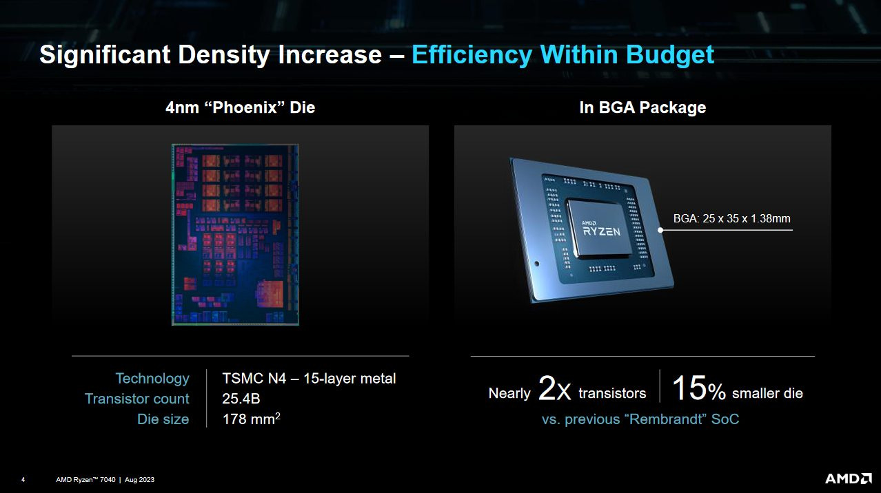
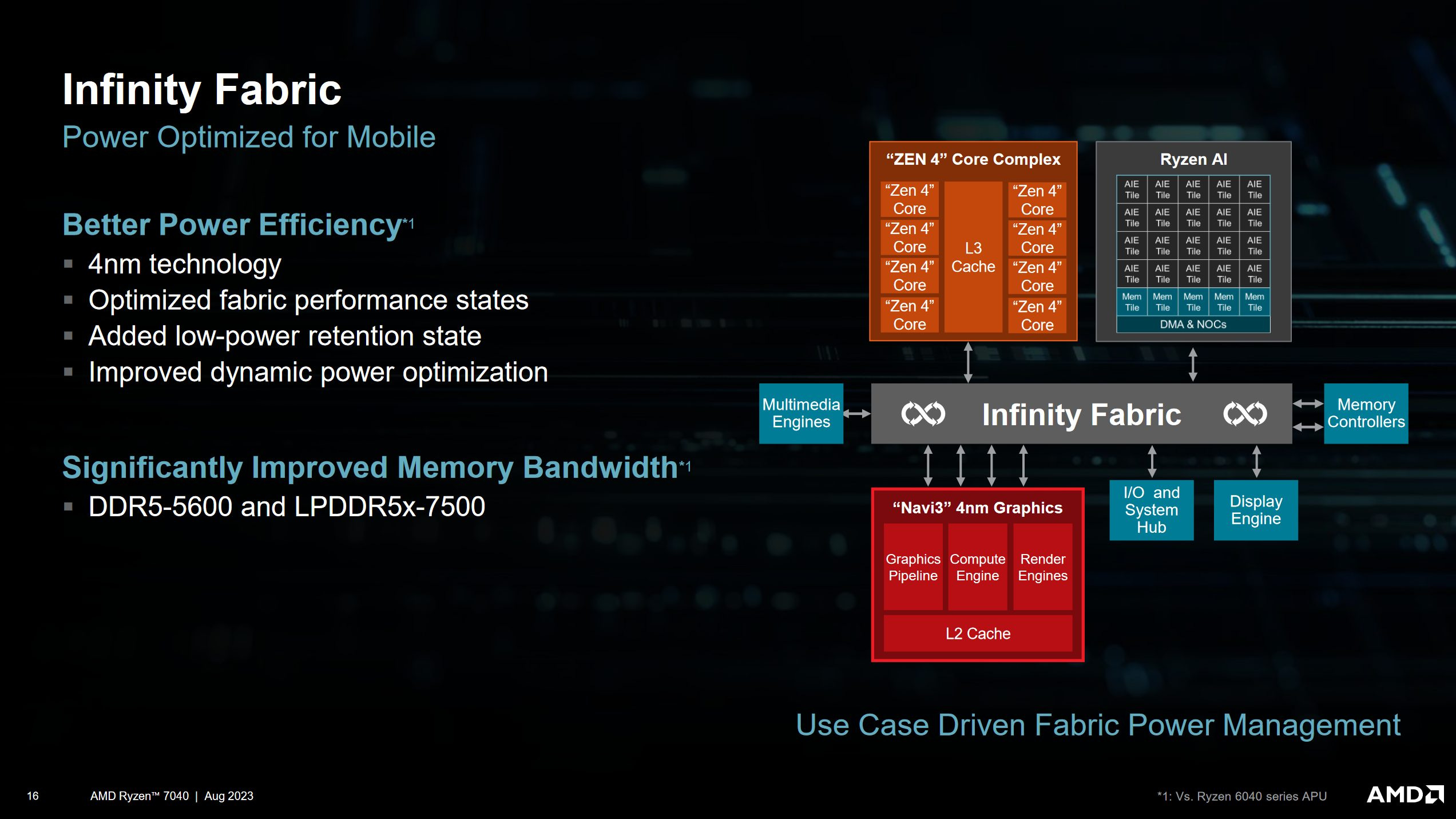
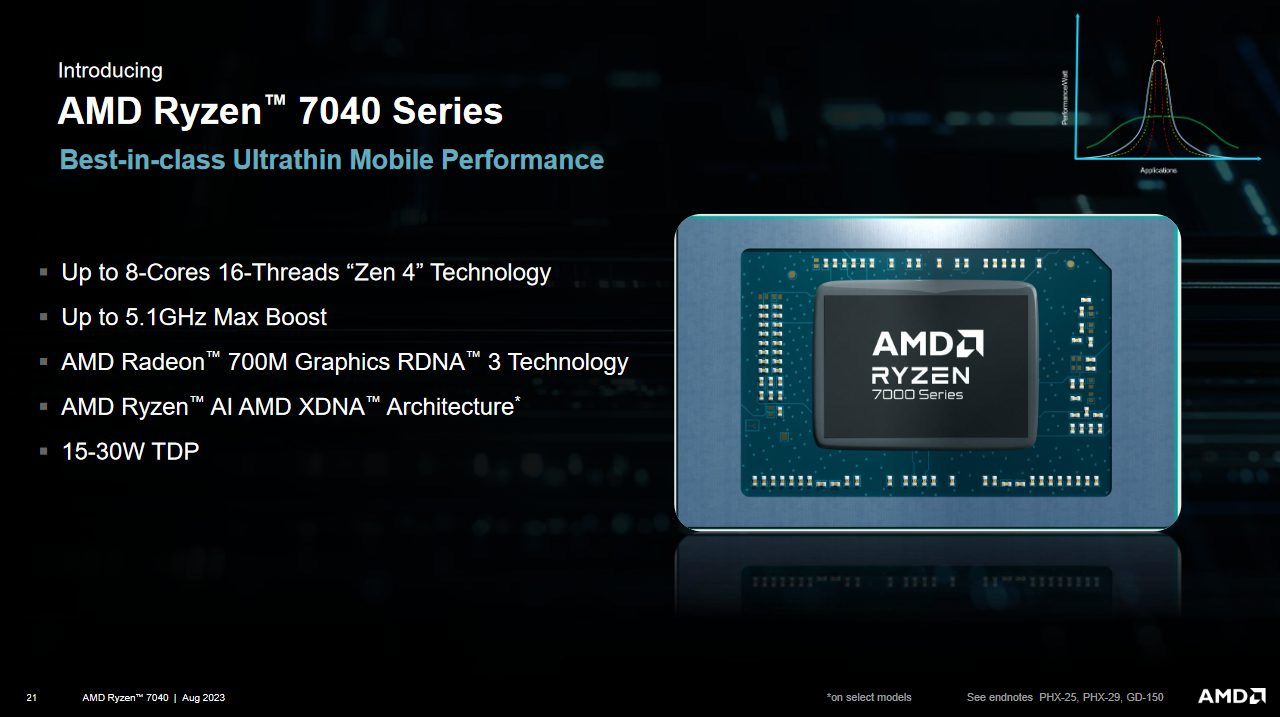
Phoenix is manufactured on TSMC’s N4 process and occupies 178 mm2. The chip has 25.4 billion transistors, and combines Zen 4 cores with RDNA 3 graphics. Alongside the all-important CPU and GPU, AMD has added several supporting IP blocks to accelerate ML inference and signal processing. Phoenix’s die ends up being smaller than AMD’s prior Rembrandt, and fits into the same 25x35mm BGA package.
CPU Side
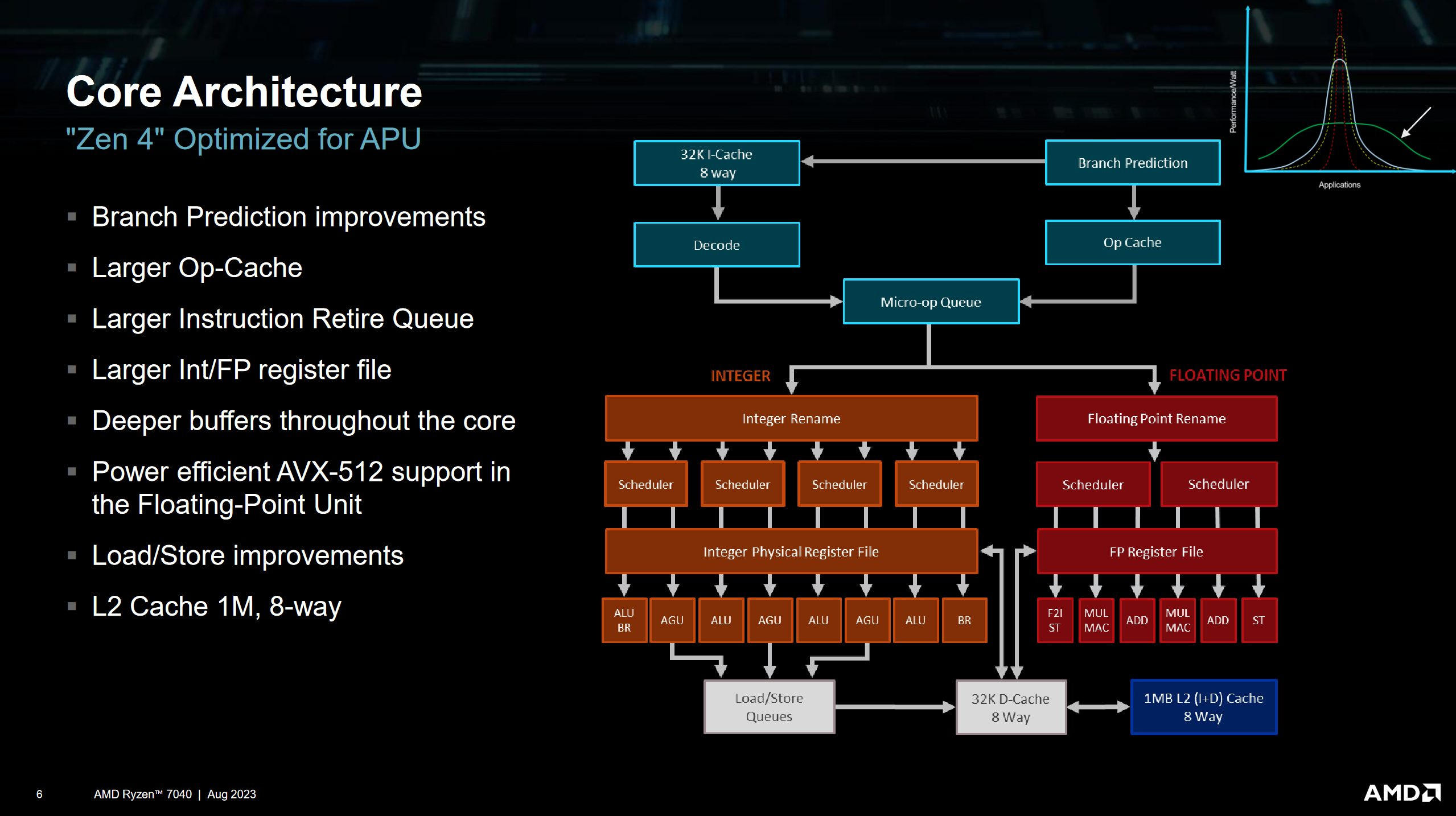
On the CPU side, Phoenix has a cluster of eight Zen 4 cores. We’re very familiar with the core architecture already, and recommend checking out our articles on that. Phoenix however has a different cache setup, with only 16 MB of L3 instead of the usual 32. AMD likely shrank the L3 slices to 2 MB per core to reduce die area usage.
From our testing, latency is identical to desktop Zen 4’s. Actual latency will be slightly worse because desktop Zen 4 clocks higher. For example, the Ryzen 9 7950X3D’s non-VCache chiplet sees 8.85 ns of latency at a 16 MB test size. The Ryzen 7 7840HS gets 10.92 ns of latency at the 10 MB test size. Part of that difference is because HP insists on limiting clock speed to 4.5 GHz, even though the 7840HS should be able to boost to 5.1 GHz.
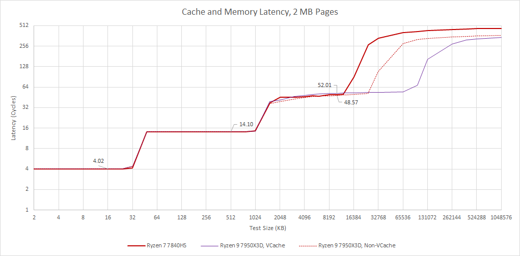
Memory latency is also higher at 103.26 ns for the 1 GB test size, compared to 87.68 ns on the 7950X3D. Memory timings play a role here, because my 7950X3D is using DDR5-5600 36-36-36-88. Laptops often have worse memory timings, and the DDR5-5600 CL46 memory used by HP is no exception.

Phoenix’s memory controller supports both DDR5 and LPDDR5. The latter is useful in handhelds where power efficiency is of paramount importance. Memory latency with LPDDR5 is higher at 119.81 ns. However, AMD has dramatically improved LPDDR5 latency compared to Van Gogh, which suffered massive latency when CPU cores accessed DRAM.
Bandwidth to Infinity Fabric
The CPU cluster interfaces with the rest of the system through a 32 byte per cycle Infinity Fabric link. Unlike desktop designs where the write path is half as wide, the CPU-to-fabric write path can also handle 32 bytes per cycle. This is very unlikely to affect real world performance, as I have seen no workload where a single core needs more than 30 GB/s of write bandwidth. A workload with more than one thread could demand more bandwidth, but can also be split across CCX-es.
Try writing zeroes and see what happens
Paraphrased, from Mahesh Subramony on the sidelines at Hot Chips 2023
Furthermore, AMD has implemented write optimizations to reduce Infinity Fabric traffic. Write bandwidth from a single 7950X3D CCD can exceed 68 GB/s when zeroing cachelines with CLZERO. Zeroing out memory is surprisingly common, because programs will initialize memory to ensure newly allocated memory starts at a known state. Operating systems will often do so as well. If applications zero memory with recognized methods, they can see higher effective write bandwidth than a generic test may suggest.
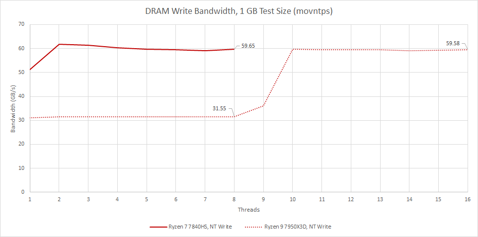
Stepping back, maximum write bandwidth is very close to that of desktop Zen 4. Read behavior is slightly different because the single cluster’s 32 byte per cycle interface can’t saturate the memory controller.
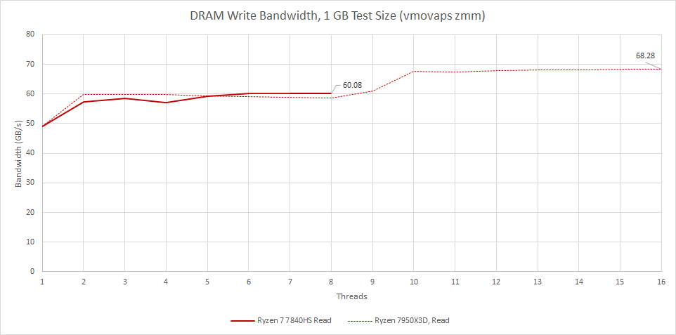
However, 60 GB/s is still plenty of bandwidth for eight cores. Caches should be absorbing the bulk of memory accesses in most client programs. Some applications may take all the bandwidth they can get, like scientific computing or machine learning, but mobile SoCs aren’t your best bet for that.
Infinity Fabric Optimizations
Infinity Fabric is AMD’s coherent interconnect. It’s critical to power efficiency because interconnect power can be a significant portion of chip power consumption, especially in workloads that aren’t pushing compute at full tilt. AMD has profiled a variety of workloads, and set up Phoenix’s Infinity Fabric to enter different operational modes based on whether a workload is compute bound, IO bound, or has very specific characteristics (like videoconferencing).
These optimizations avoid Van Gogh’s problems, where it was limited to around 25 GB/s of CPU-side bandwidth, thanks to an Infinity Fabric implementation heavily optimized for gaming within a tiny power budget. On Cheese’s HP laptop, Infinity Fabric clock varies depending on workload:
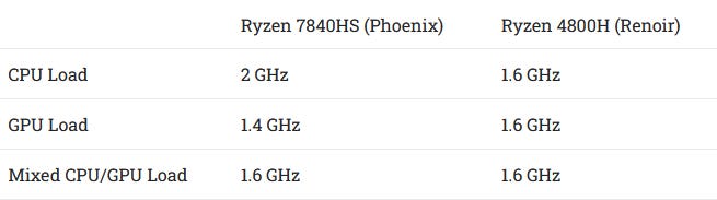
My suspicion is AMD’s using low fabric clocks to improve energy efficiency when the GPU’s pulling a lot of bandwidth. The GPU has four 32B/cycle ports to fabric, letting it get enough memory bandwidth even at low fabric clock. CPU workloads are given higher fabric clocks because client programs tend to be more sensitive to latency than bandwidth, and higher fabric clock improves latency. Phoenix’s variable Infinity Fabric clocks contrast with Renoir’s, where fabric clock goes to 1.6 GHz regardless of what component is generating memory traffic.
To further save power, AMD aggressively pursues power and clock gating opportunities. A new Z8 sleep state allows power and clock gating for brief periods of idleness, like between keystrokes, with imperceptible wake time. Phoenix can achieve high residency in Z8 state during video playback, suggesting the media engine’s buffers and caches are large enough to let it make memory accesses in short bursts.
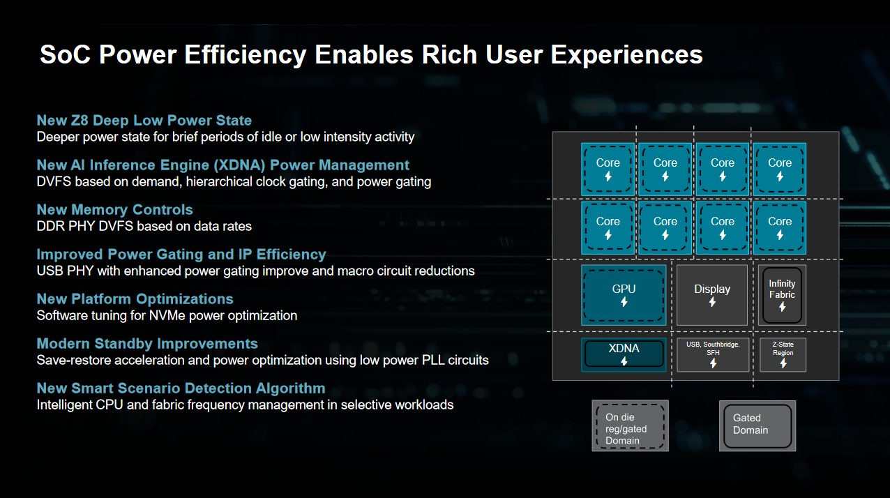
Additional power savings come from optimizing various physical interfaces. Memory controllers can dynamically change clock and voltage states depending on how much traffic they have to serve. A USB 2.0 interface that AMD has been using for years turned out to have a lot of power optimization opportunities, so AMD tuned that as well.
GPU Side
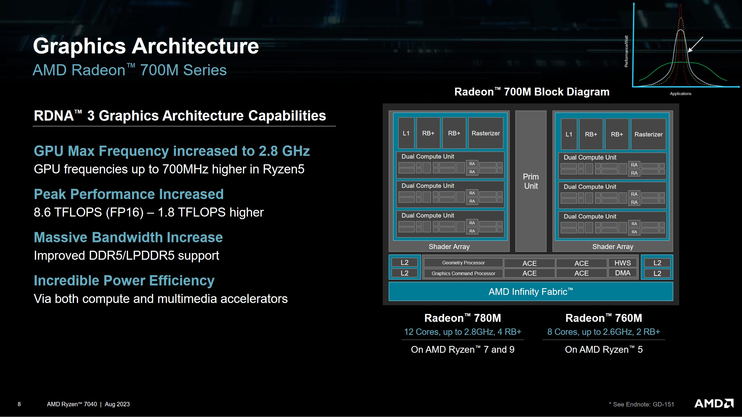
Phoenix’s GPU is based on AMD’s current-generation RDNA 3 architecture, and gets a proper “Radeon 780M” moniker rather than just being called Vega or gfx90c. It features six WGPs for a total of 768 SIMD lanes, capable of 1536 FP32 operations per cycle. These are divided into two shader arrays, which each have 256 KB of mid-level cache. A 2 MB L2 cache helps insulate the iGPU from DRAM, and is pretty important to the iGPU’s performance. Compared to Van Gogh, Phoenix has twice as much L2 cache, slightly more memory bandwidth, and 50% more SIMD lanes.
To get a sense of how disproportionately big Phoenix’s L2 cache is, AMD’s RX 7600 discrete GPU also has 2 MB of L2 cache, as does Nvidia’s old RTX 3050.
Latency at L0, L1, and L2 is quite similar when compared to the RX 7600, though the discrete card is slightly faster thanks to higher clock speeds.
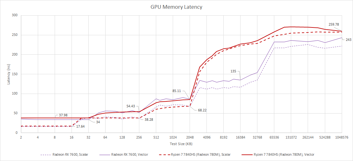
Past L2, Phoenix’s iGPU suffers much higher latency because it lacks an Infinity Cache. (LP)DDR5 gives the iGPU a better bandwidth per SIMD operation ratio than that of desktop GPUs, so dedicating area towards another level of cache can’t be justified.

DDR5’s bandwidth really can’t be understated. With DDR5-5600 or LPDDR5-5600, Phoenix can achieve higher GPU-side DRAM bandwidth than Nvidia’s GDDR5 equipped GTX 1050 3 GB from several years ago. 5.6 gigabits per pin is also faster than some early GDDR5 implementations.
If GPU-side memory accesses hit cache, Phoenix’s iGPU enjoys several times as much L2 bandwidth as Van Gogh.

For perspective, Nvidia’s flagship GTX 980 Ti from 2015 gets 686.9 GB/s of L2 bandwidth in the same test. Phoenix won’t have to worry about L2 bandwidth issues at all, even with its large shader array.
Unlike top end desktop RDNA 3 parts, the iGPU runs the frontend and shader array at the same clock. With smaller GPUs, AMD did not see much benefit in clocking the work distribution hardware faster, because the shader array is often the bottleneck. We already saw signs of this on AMD’s RX 7600, and Phoenix’s iGPU has an even smaller shader array.
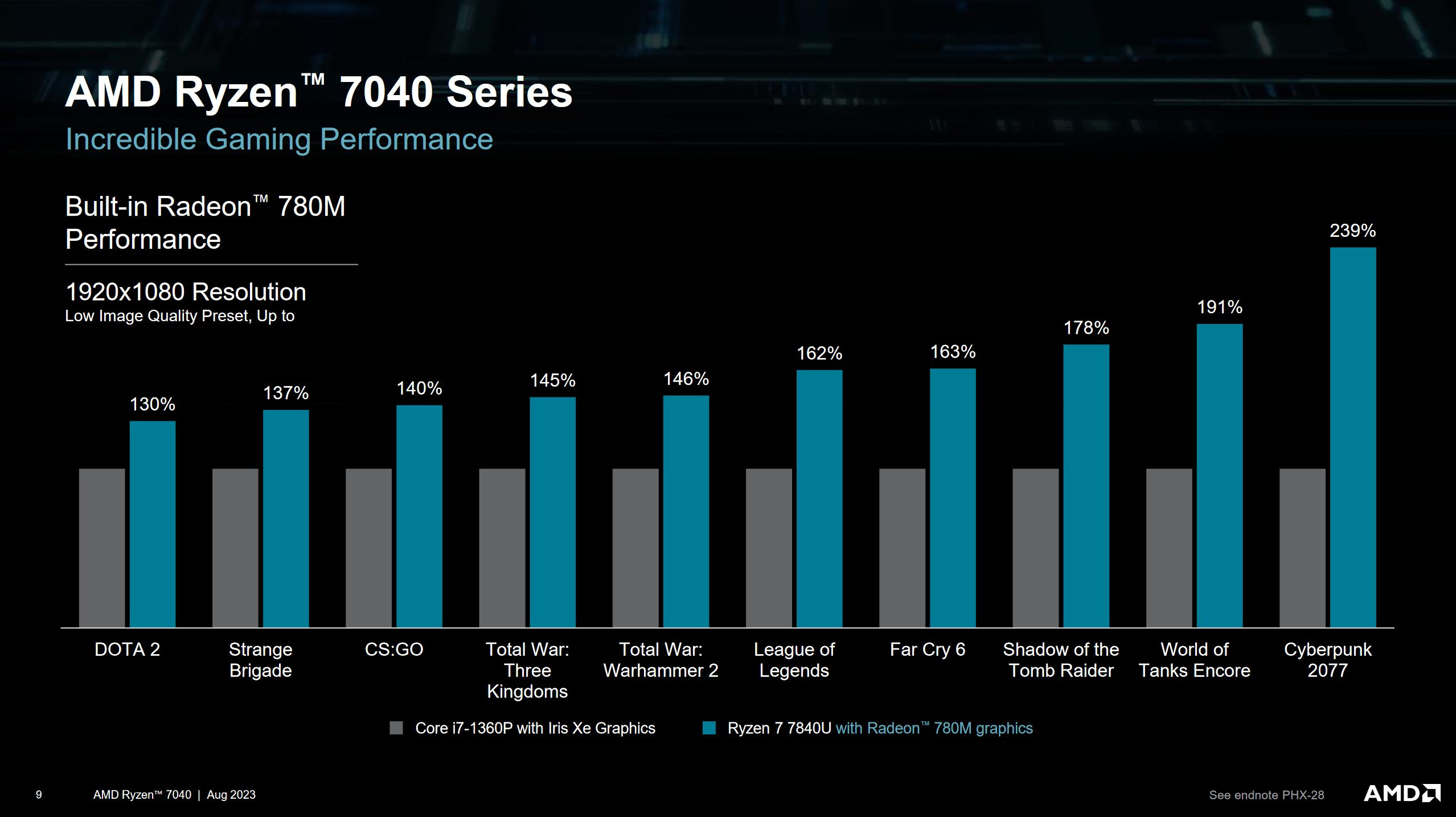
Valve’s Steam Deck already demonstrated how a lot of PC games can run on a handheld. Phoenix’s iGPU is wider, faster, and enjoys more bandwidth than the Steam Deck’s. AMD didn’t provide framerate figures, instead choosing to show Phoenix’s performance advantage over Intel’s iGPU. But given the Steam Deck’s performance, I expect Phoenix to deliver playable framerates at 1080P or 720P with some settings turned down.
Video Engine
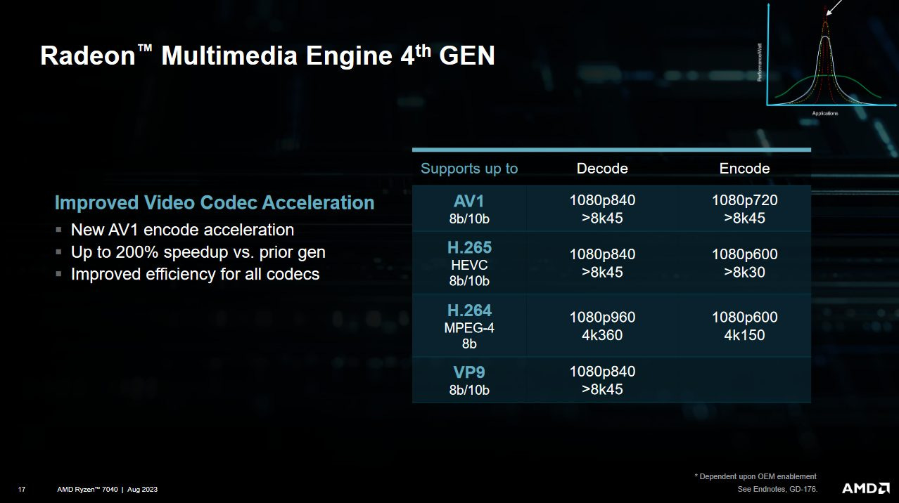
Even if it’s not used for gaming, RDNA 3 comes with a AV1-capable video engine, making Phoenix more future proof as next-generation video codecs start to gain traction. While the engine is not new, AMD did reveal that it uses a race-to-idle scheme to save power. It also has enough throughput to handle several simultaneous video streams, which is important for videoconferencing.
XDNA AI Engine
Machine learning has taken off in the past few years, and AMD has put an AI engine (XDNA) on Phoenix to accelerate inferencing. XDNA is built from AIE-ML tiles using a Xilinx developed architecture. Phoenix’s XDNA implementation has 16 AIE-ML tiles, and can be spatially partitioned to let multiple applications share the AI engine.
AMD didn’t go into specifics of the AIE architecture, but thankfully documentation is public.
XDNA aims for enough throughput to handle small ML loads while achieving very high power efficiency. It runs at very low clock and uses very wide vector execution. Documentation suggests a 1 GHz clock, but Phoenix’s XDNA might be running at 1.25 GHz as AMD says BF16 is supported with 5 TFLOPS of throughput. To drive the very wide vector units, XDNA has two vector register files. One 6 KB set of registers provides multiplier inputs. A separate 8 KB register file holds accumulator values and is accessed at a later stage in the multiply-add pipeline. Both register files can be addressed in 1024-bit, 512-bit, or 256-bit modes, with consecutive 256-bit registers forming a 512-bit or 1024-bit one.

Multiply-add operations seem to have 5-6 cycle latency depending on whether you need FP normalization. It’s a bit long for something running around 1 GHz, but XDNA gives you permutes as part of the deal. Simpler 512-bit adds and shuffles enjoy faster 3 cycle latency.
Each XDNA tile feeds its massive vector units with 64 KB of directly addressed data memory. The data memory is not a cache, saving power because no tag checks are needed. Further power savings come from using 20-bit addressing, which ought to be enough for anyone. Addresses are generated by three AGUs, which operate on 20-bit pointer and modifier registers. Using separate registers for addresses is nothing new (the 6502 had two index registers), and avoids needing six extra ports on the main scalar register file.

After addresses are generated, the data memory can handle two 256-bit loads and one 256-bit write per cycle. XDNA enjoys the same bandwidth when accessing data memory on neighboring tiles, which gives a single tile high bandwidth access to 256 KB of memory. XDNA can save significant memory bandwidth (and computational power) with support for 50% sparsity, though ML models have to be developed with sparsity in mind to see benefits. The memory subsystem can decompress sparse matrices, and mask registers let the vector units avoid pointless calculations.

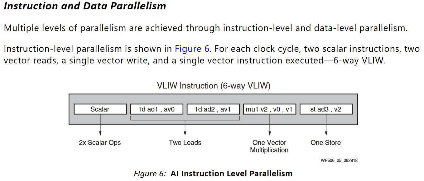
At the frontend, each XDNA tile has 16 KB of program memory for instruction storage. Again, this isn’t a cache, so power is saved by avoiding tag checks and using fewer address bits. VLIW instruction formats allow simple decode logic while letting the frontend bring in up to six instructions per cycle, as long as they’re in the right mix. A VLIW bundle with 6 instruction occupies 16 bytes, but bundles can be shorter too if not all of the slots are needed.
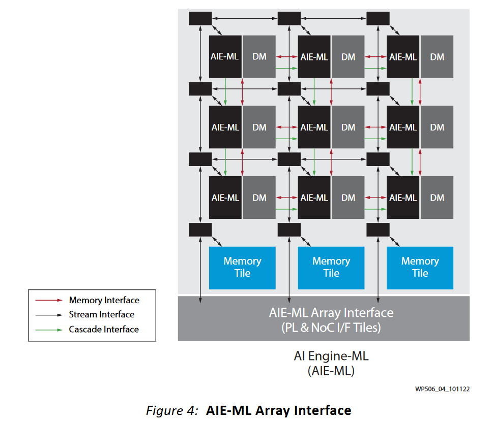
At the engine level, XDNA uses a specialized interconnect and memory subsystem. I already mentioned how each tile can directly access data memory on its neighbors with very high bandwidth. But that’s not it. Tiles can forward accumulator outputs to their neighbors too, with dedicated 512-bit interfaces. A general AXI4 interface allows more generic transfers between tiles, and crossing tile boundaries happens with two cycle latency. The whole engine has a shared block of L2 SRAM, which acts as staging memory. AMD didn’t disclose the L2 SRAM size, but I suspect it’s a row of four memory tiles. Each memory tile has 512 KB of capacity, so Phoenix’s XDNA engine could have 2 MB of L2 SRAM.
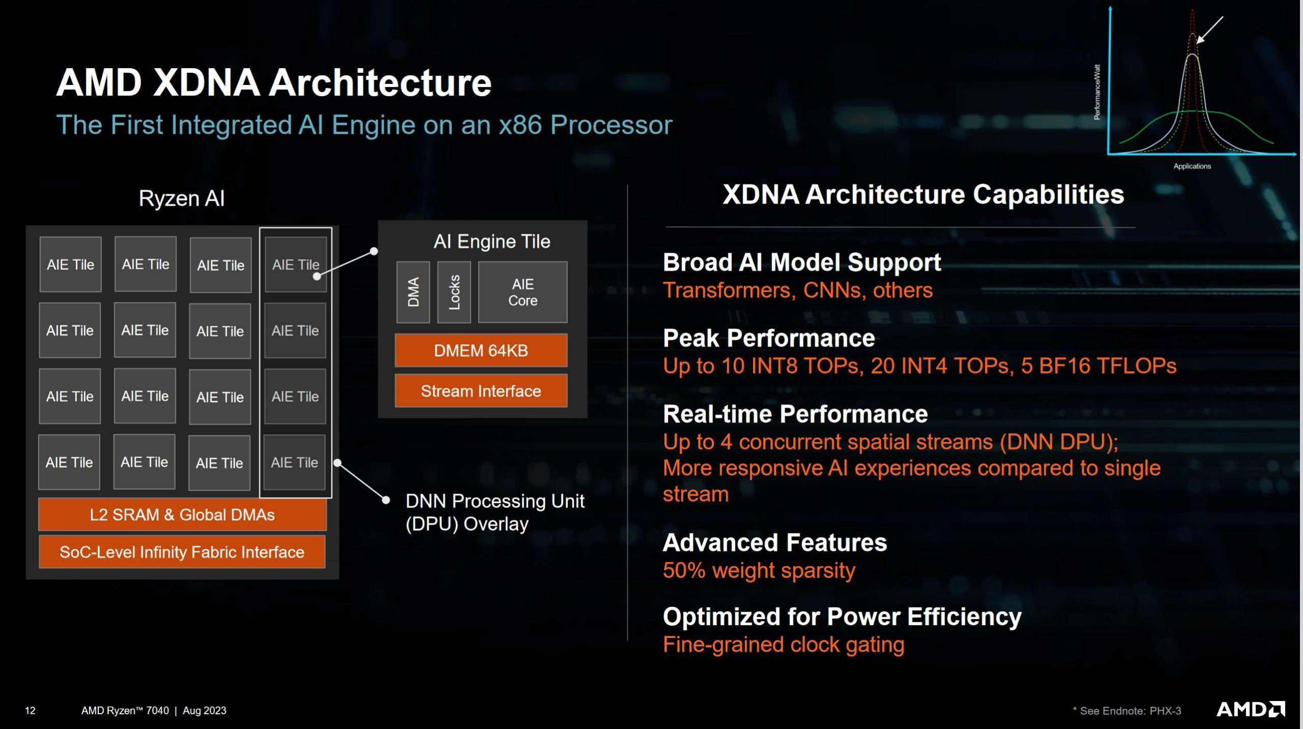
System memory is accessed via DMA, which streams in data using a 32-byte per cycle port to Infinity Fabric.
If applications take advantage of it, XDNA should let Phoenix handle AI workloads with better power efficiency than the GPU. Technically, the RDNA 3 iGPU can achieve higher BF16 throughput with WMMA instructions. However, doing so would likely require a lot more power than the more tightly targeted XDNA architecture. Saving every bit of power is vital in a mobile device running off battery, so XDNA should let programs use AI with minimal power cost. AMD says most applications they’re targeting are friendly to INT8 operations, and XDNA should provide massive throughput there.
Zooming up, AMD’s Xilinx acquisition is starting to bear fruit. Previously, AMD’s smaller company size and lower budget meant they had less capability to branch out into side projects. AMD’s mobile chips had no answers for Intel’s GNA or IPU. XDNA is a step in the right direction, and gives AMD a potent accelerator for machine learning.
Audio Co-Processor
As you might have noticed, offloading processing to dedicated accelerators is a becoming a favored way to improve power efficiency. Phoenix goes further than offloading AI by offloading audio processing too. In fact, you could run AI noise reduction on the audio coprocessor if you can fit it within its two DSPs.
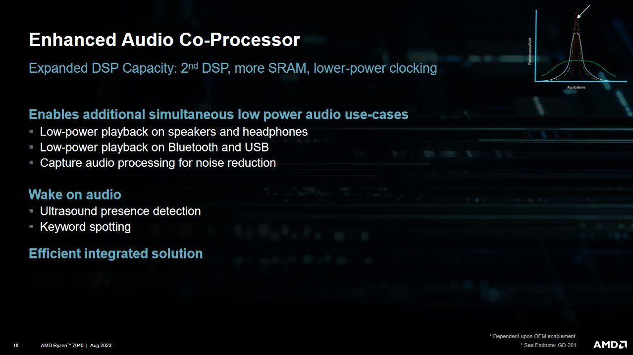
The audio processor can run at a very low clock while it’s being used as a wake source. With voice assistants playing a role across several operating systems, this could potentially save a lot of power.
Another cool use of low power, always-on DSPs is using ultrasound sonar to detect humans. AMD’s ultrasound runs at above 20 KHz but below 35 KHz, letting it get through the microphone and speaker’s band pass filters. Then, it can use Doppler shift to distinguish human movement from static objects in the same way that a look-down radar filters out ground clutter.

AMD has opened up this ultrasound engine to third parties. As another note, dog hearing can cover the 20-35 KHz range, so the ultrasound engine may be able to detect static dogs by making them non-static, after which they will cause a Doppler shift.
Final Words
Phoenix is the latest addition to AMD’s long line of APUs (chips with integrated graphics). Ever since Picasso launched with Zen cores and Vega graphics, AMD’s APUs saw massive improvements from generation to generations. That’s largely because AMD started from so far behind. But Zen 2 and Zen 3 APUs were already very solid products, so Phoenix’s improvements make it a very dangerous competitor.
AMD has put a lot of focus into reducing power consumption across every area of the chip. Zen 4 cores do an excellent job on the CPU side, while RDNA 3 provides strong graphics performance. Hardware offload helps power efficiency on specialized AI and audio processing workloads. To support all this, Infinity Fabric gets lower power states and very flexible clock behavior. Phoenix ends up being able to perform well across a wide range of form factors and power targets.
Today, Phoenix has already surfaced in a variety of products. These include handhelds like ASUS’s ROG Ally, along with a variety of laptops and mini PCs. AMD now has a mobile CPU ready to take on Intel’s best, and Intel should be worried.
We’d like to thank AMD for putting together an excellent presentation at Hot Chips 2023, and hope to see their mobile efforts reach even further in the future.
If you like our articles and journalism, and you want to support us in our endeavors, then consider heading over to our Patreon or our PayPal if you want to toss a few bucks our way. If you would like to talk with the Chips and Cheese staff and the people behind the scenes, then consider joining our Discord.