
Cortex X2: Arm Aims High

Arm has traditionally targeted the low end of the power and performance curve, but just as Intel has been looking to expand into the low power market, ARM is looking to expand into higher power and performance segments. The Cortex X series is at the forefront of this effort.
Delivers ultimate peak performance within an expanded envelope for power and area.
Here, we’ll be looking at the Cortex X2 as implemented in the Snapdragon 8+ Gen 1. This SoC features a single X2 core, alongside four Cortex A510 and three Cortex A710 cores. The Cortex X2 in this SoC typically runs at 2.8 GHz, although lscpu indicates its clock speed can range from 787.2 MHz to 3.187 GHz.

When placed under load, the Cortex X2 quickly boosts to an intermediate clock speed of 2.56 GHz. After 55 ms, it reaches 2.8 GHz. No higher clock speeds were observed when testing over a longer duration.
Core Overview
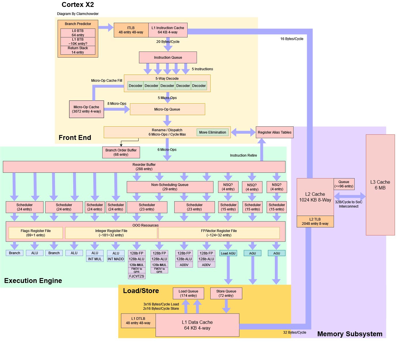
Cortex X2 is similar to its 7-series cousin, the Cortex A710, but is substantially larger. X2 has more reordering capacity, a wider pipeline, and more execution units. Despite these changes, X2 has a 10-stage pipeline just like A710.
Branch Prediction
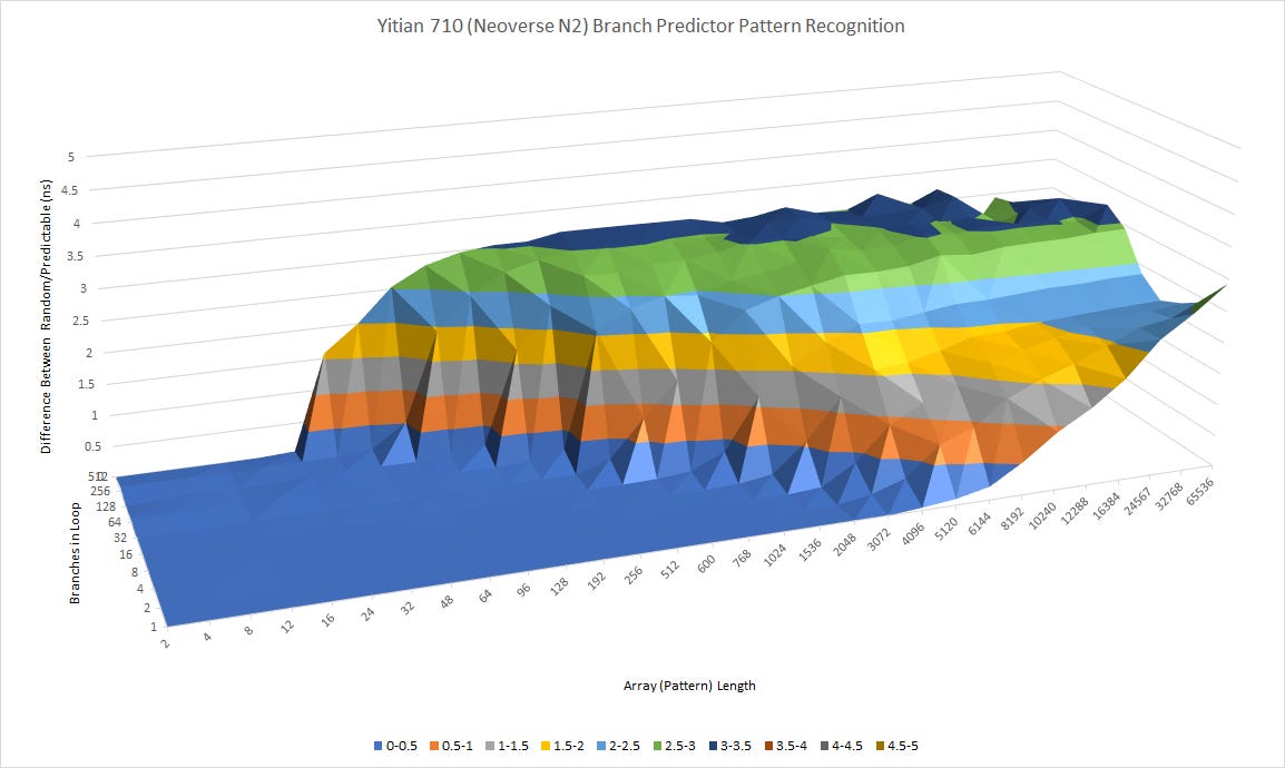
Branch prediction is important for any CPU because wasted work from mispredicts will hurt both performance and power efficiency. Cortex X2 gets more area and power budget than other ARM cores, and therefore gets a more capable branch predictor. It can recognize somewhat longer patterns than Cortex A710 and its server cousin, Neoverse N2. Alongside that, it does better when there are a ton of branches in play.

However, ARM’s statement that X2 has an “expanded envelope for power and area” has to be taken in context. X2 still goes into mobile chips even if high end SoCs only feature a single X-series core. Passive smartphone cooling means X2 is still working within a much tighter power budget than desktop CPUs. AMD’s Zen 4 in comparison pulls all the stops to maximize branch prediction accuracy.


The branch predictor’s job is to make sure the frontend is well-fed with fetch addresses. Accurately predicting branch direction is one component of this. Another component is delivering those fetch addresses quickly. To do so, the branch predictor keeps a cache of branch destinations, called a branch target buffer (BTB).

Cortex X2’s BTB is mostly unchanged from A710’s. A micro-BTB can handle two taken branches per cycle, and can track up to 64 branches. Then we see about 10K branches tracked with 1-2 penalty cycles. Returns are handled with a 14 entry return stack as well.
Frontend: Fetch and Decode
Cortex X2 has an enlarged version of A710’s frontend, and enjoys both increased caching capacity and higher throughput. The micro-op cache grows to 3072 entries, making it larger than Sunny Cove’s. Also, X2 mandates a 64 KB instruction cache, while A710 implementers could pick between 32 KB or 64 KB instruction cache.

Compared to AMD’s Zen 4, X2’s micro-op cache is smaller, but its larger instruction cache is a notable advantage for larger code footprints. If code footprints exceed 32 KB (but not 64 KB), and have a lot of unpredictable branches, Zen 4 will suffer from L2 latency and see a lot of frontend bubbles.
In terms of throughput, X2’s micro-op cache can provide 8 operations per cycle, which is more than enough to feed the 6-wide renamer downstream. The 5-wide decoder can provide generous instruction throughput for larger code footprints and compares favorably to the 4-wide decoders found on Zen 4 and A710. X2 can sustain more than four instructions per cycle even when running code from L2.

However once you get past L2, Zen 4 pulls ahead again. Thanks to AMD’s very high performance L3 and an aggressive branch predictor, Zen 4 can sustain over 3 IPC when running code from L3. Cortex X2 doesn’t do badly and can still average 1.66 IPC in that case.
Out of Order Execution
After micro-ops from the frontend have been renamed, out-of-order execution tracks and executes them as their data dependencies become available. X2 has a much larger OoO engine than A710 while enjoying similar instruction fusion optimizations. ROB size increased to 288 entries with other structure sizes scaled up to match.

X2 ends up getting close to Zen 4 in most areas, and even exceeds it in a few. ARM’s core can keep a staggering number of loads in flight. Instruction fusion allows it to track 249 FP operations pending retirement, while Zen 4 can only track 154. However, Zen 4 does better if 512-bit vectors are used because its large AVX-512 register file lets it keep a lot more explicitly parallel work in flight.
A710 had an overbuilt scheduler considering its ROB capacity and other structure sizes. Cortex X2 brings things back into balance. Integer scheduler capacity is surprisingly similar to Zen 4’s, with four 24 entry queues. Zen 4 shares those scheduler queues with the AGUs, while Cortex X2 has separate AGU schedulers.
FP/Vector Execution
Arm’s Cortex 7 series cores had weak vector execution thanks to tight area and power constraints. Cortex X2 uses its larger power and area budget to implement a quad-pipe FP and vector setup. All four pipes can handle common math operations and enjoy the same low floating point execution latency that Cortex A710 does. Cortex X2 is therefore a very strong contender for scalar or 128-bit vector operations.
I wasn’t able to fully utilize all four pipes even with instructions that should have been able to do so (according to the optimization guide), but even so, throughput is very good.

Zen 4 still has an advantage with longer vector lengths and lower latency for vector integer operations. But even if Zen 4 uses 256-bit vectors, Cortex X2 can put up a decent fight because it has identical theoretical throughput (per cycle) for common operations. For example, Zen 4 can do two 256-bit FMAs per cycle. Cortex X2 can match that by doing four 128-bit FMAs. AMD’s core also enjoys better scheduling capacity. X2 seems to have a pair of 23 entry schedulers. I couldn’t find any operations that only go to one of the ADDV pipes, so I can’t tell if it’s a single 23 entry queue, or a 11+12 entry setup. I think a pair of dual port schedulers is more likely. AMD’s Zen 4 uses a pair of 32 entry schedulers, giving it 64 FP scheduling entries compared to Cortex X2’s 46.

Like Zen 4, X2 has a non-scheduling queue (NSQ) in front of the FP schedulers, which lets the core track more incomplete operations without using a larger scheduler. An NSQ can contain a lot more entries than a scheduling queue, because it doesn’t have to check each entry each cycle to see if it’s ready for execution. With its 29 entry NSQ, Cortex X2 can keep a total of 75 incomplete FP operations in flight. X2 is an improvement over A710, but AMD prioritizes FP execution more. Zen 4 uses a larger 64 entry non-scheduling queue and can keep a total of 128 incomplete FP operations in flight.
Memory Execution
Cortex X2 handles memory accesses with three address generation units (AGUs), with some similarities to A710 and Zen 4. The memory subsystem can handle three memory accesses per cycle, of which three can be loads and two can be stores. Its scheduling setup appears similar to the one on Neoverse V2, but with slightly smaller scheduling queues and tiny non-scheduling queues in front of them.
After addresses are calculated, the load/store unit has to ensure they appear to execute in program order. Loads might have to get their data from prior in-flight stores. Ideally, data from the store gets sent to a dependent load with minimal delay. But detecting dependencies can be complicated because loads and stores can overlap without matching addresses.
Cortex X2 acts a lot like prior ARM cores starting from Neoverse N1. The load/store unit can forward either half of a 64-bit load to a dependent 32-bit store, but can’t handle any other cases. Fast-path store forwarding has a latency of five cycles, while the slow path incurs a 10-11 cycle penalty.

Zen 4 has a far more robust mechanism for resolving memory dependencies. Any load contained within a prior store can have its data forwarded, and exact address matches can be handled with zero latency. ARM is falling a bit behind here with essentially pre-2010s forwarding capability on a core design going for ultimate performance. However, the slow fallback path on Zen 4 is more expensive at 19-20 cycles, likely indicating Zen 4 has more pipeline stages between between address calculation and store retirement.
Cortex X2 does better with avoiding misalignment penalties. Zen 4’s data cache has 32B store alignment, so stores that cross a 32B aligned boundary have a throughput of one per two cycles. X2 doesn’t see any penalty unless accesses cross a 64B cacheline boundary.
Henry Wong experimented with smaller load and store sizes and didn’t see a significant difference. However, vector loads do behave differently on on some CPUs. Cortex X2 can again forward either 64-bit half of a 128-bit store, but curiously can also forward the low 32 bits and merge that with another 32 bits from the data cache to quickly complete a partially overlapping 64-bit load.

Zen 4’s vector side acts a lot like the scalar integer side, but with a couple cycles of additional latency. AMD can impressively handle misaligned loads with no cost, but again is more prone to hitting misaligned store penalties than Cortex X2.

Address Translation
User programs don’t directly address locations in DRAM. Instead, they use virtual addresses, and the operating system sets up a map of virtual address to physical addresses for each process. This allows cool things like swapping to disk when physical memory runs low. However, hardware has to translate addresses on the fly while maintaining high performance. Translation lookaside buffers (TLBs) cache virtual to physical address mappings. TLB hits let the CPU avoid traversing the operating system’s paging structures, which would turn one memory access into several dependent ones.
Cortex X2 has a two-level TLB setup. The first TLB level has 48 entries and is fully associative. It’s a welcome size increase over the 32 entries in A710, but is still smaller than Zen 4’s 72 entry DTLB.

L1 DTLB misses can be caught by Cortex X2’s 2048 entry L2 TLB, with a cost of 5 extra cycles. This is a welcome improvement over the Cortex A710’s 1024 entry TLB, and Neoverse N2’s 1280 entries. Cortex X2’s improved TLB sizes let it incur less address translation latency for programs with larger data footprints. It’s still a step behind Zen 4’s 3072 entry L2 TLB, but it matches Zen 2.
Cache and Memory
Caching is an important component of a CPU’s performance. In the Snapdragon 8+ Gen 1, Cortex X2 gets a triple level cache hierarchy. The large 64 KB L1D has 4 cycle latency. It’s not the best for a CPU clocked below 3 GHz, considering the old AMD Athlon and Phenom CPUs achieved 3 cycle L1D latency years ago. As a consolation, indexed addressing doesn’t cost an extra cycle like on recent AMD and Intel CPUs.

Arm mandates a 64 KB L1D on Cortex X2, but lets implementers configure the L2 with 512 KB or 1 MB of capacity. The L2 is inclusive of the L1D, so Arm is making a good decision in not offering smaller L2 options. Both L2 configurations have 8-way associativity, so Arm is changing capacity by increasing the number of sets. Qualcomm picked the 1 MB option on the Snapdragon 8+ Gen 1. L2 hits have 11 cycle latency, which comes out to just under 4 nanoseconds. Cortex X2 can’t clock as high as Zen 4, but the short L2 pipeline helps close some of the gap. Just like the L1D, the L2 is always ECC protected. I’m glad Arm isn’t making ECC protection optional.
The L2 has a 256-bit bus to the DSU-110, which connects cores to the rest of the system. Arm lets implementers configure the DSU-110 with up to 16 MB of L3 cache. The L3 is 16-way set associative with power of two capacities, or 12-way set associative if capacity is divisible by 3. Qualcomm in their infinite wisdom has chosen 6 MB of L3 cache, so the Snapdragon 8+ Gen 1’s L3 is 12-way set associative.
The L3 is arranged into slices, and is filled by victims from core private caches. Cortex X2 suffers higher L3 latency than Zen 4. At the 4 MB test size, its 18.18 ns result is similar to the 17.41 ns seen by the Intel Core i9-12900K’s E-cores. A small 6 MB cache should make up for its lack of capacity by at least being fast, but I suppose that would be asking too much from a mobile SoC. At least it’s reasonable from the ~51 core cycle latency.

Arm’s Technical Reference manual suggests five to seven cycles are spent accessing L3 data storage, so the remaining cycles are spent checking tags, traversing the interconnect, and at upper level caches. Program-visible L3 latency includes time spent accessing the L2 TLB, since the L1 TLB is not large enough to cover the L3 cache.
At the 1 GB test size, we see 202 ns of DRAM latency. L2 TLB misses and page walks add potentially heavy address translation latency on top, but separating that from DRAM latency is difficult because there’s no way to use huge pages on Android. It’s not too bad for a cell phone SoC, but is a world apart from desktop or laptop CPUs. It’s also worse than Apple’s M1, which should worry Qualcomm because Apple shares designs across phones and tablets.

Apple’s 12 MB shared L2 serves the same role as the Snapdragon 8+ Gen 1’s 6 MB L3, but has both higher capacity and lower latency. I wonder how Cortex X2 would do if it were better fed.
Bandwidth
Cortex X2’s three AGUs and triple port data cache allow it to service three 128-bit accesses per cycle. The core therefore can get the same per-cycle L1D bandwidth as A710 and Apple’s M1, and beats older Arm cores like the Neoverse N1 by a large margin. Apple’s M1 still gets an absolute bandwidth lead thanks to higher clocks. Compared to recent x86 cores, X2’s L1D bandwidth is still low due to lower clocks and lack of wider vector support.

L2 bandwidth is decent at 28 bytes per cycle. It’s close to Apple M1’s L2 bandwidth. Zen 4 and Skylake again enjoy a large L2 bandwidth lead over Cortex X2 thanks to higher clock speeds.

L2 misses go into a transaction queue with size configurable from 72 to 96 entries. The large transaction queue helps the core cope with high L3 latency, so X2’s L3 bandwidth is on par with Skylake. DRAM bandwidth from the single Cortex X2 core is decent at 32.5 GB/s, hinting at the L3’s ability to track a lot of pending misses. The DSU-110’s CHI (Coherent Hub Interface) can track up to 128 reads per master port. If Qualcomm is using that to connect memory controllers, it would explain the decent memory bandwidth in the face of high latency.
Write Bandwidth
We can examine bandwidth without latency restrictions by testing writes instead of reads. Normally, writes have much lower bandwidth because a write access involves a read-for-ownership first to fill the line into cache. However, Cortex X2 detects when entire cachelines are being overwritten without any of the data getting read. If that happens to enough consecutive lines, the core’s bus interface switches into write streaming mode. In write streaming mode, cache misses don’t cause fills and simply write out the data. Thus, writes won’t be held back by read latency and RFO bandwidth won’t compete with writebacks.

Bandwidth from L1D is lower because only two AGUs can handle writes. But every lower level in the cache hierarchy benefits. L2 bandwidth goes up to 30 bytes per cycle, while L3 bandwidth reaches 67 GB/s. Finally, DRAM bandwidth sits around 41.2 GB/s. I suspect that’s a better reflection of what the memory controller can deliver using its 64bit LPDDR5-6400 interface.
Final Words
Arm’s Cortex X line reaches for higher performance with an increased power and area budget. Cortex X2 is the second member of that line. It apparently has an area of about 2.1 mm2, making it just slightly smaller than Zen 4c. While Arm tries to move up the performance ladder, Intel and AMD are trying to move down to hit lower power and area targets. Arm’s efforts to move up the performance ladder mean it’s starting to overlap with AMD and Intel as those x86 companies try to move down into lower power and area targets.
AMD, Arm, and Intel share another commonality. They all have to maintain multiple cores to broaden their coverage of performance targets. AMD has the most modest and cost efficient approach. Zen 4c uses a different physical implementation of the Zen 4 architecture to reduce core area at the cost of clock speed. Intel goes all the way for maximum flexibility. Gracemont is a completely different core than Golden Cove, so Intel is splitting engineering effort between two core lines. Arm lands in the middle. Cortex X2 is a scaled up A710. The two cores have similar scheduler layouts and instruction fusion optimizations, so they’re really siblings rather than completely different designs. Some of Arm’s engineering effort can be shared across both cores, but additional time has to be spent tuning and validating A710 and X2.
To build Cortex X2, Arm took everything in A710 and moved the sliders up. Out-of-order structures enjoy increased capacity. L1, L2, and micro-op cache sizes get larger. X2 gets a quad pipe FPU, giving it a welcome upgrade over A710’s dual pipe one. Floating point units are area hungry because FP operations involve several basic operations under the hood, so X2’s larger area budget is getting put to good use. The L2 TLB is another good use of extra area. A710’s 1024 entry L2 TLB was small by modern standards, so X2’s 2048 entry one is great to see.
Cortex X2 is therefore a cool showing of what Arm’s out-of-order architecture can do when allowed to stretch its legs. Arm’s engineers have made good use of their increased area and power budget to patch up A710’s weakest areas. Newer Cortex X cores carry forward X2’s strengths while using increased transistor budgets to continue patching weaknesses.

I like where Cortex X is going and can see Arm putting pressure on AMD and Intel to keep up the pace. But when your core is stuffed into a SoC with a slow L3 and horrible DRAM latency, it’s going to suffer even when core width and structure sizes look competitive. I hope future implementations will better showcase Cortex X’s potential.
If you like our articles and journalism, and you want to support us in our endeavors, then consider heading over to our Patreon or our PayPal if you want to toss a few bucks our way. If you would like to talk with the Chips and Cheese staff and the people behind the scenes, then consider joining our Discord.
Your code seems to do 20 instructions, two blocks of 10 instructions. So the throughput will actually be min(10/latency, throughput) which corresponds to the 2.5 result above. Doing 16 independent instructions make the throughput goes to 4 IPC as advertised.
Some other tests are showing 2.53 too.