
Arm’s Cortex A510: Two Kids in a Trench Coat

Arm’s 5-series line moves slowly. The Cortex A53 and A55 each served across multiple generations of 7-series companions, and both were 2-wide in-order cores running at low clocks. When your architecture is only expected to handle non-demanding background tasks, you don’t need to push the performance envelope. But as Arm evolved the ARM instruction set, they needed a little core companion that could keep pace. The Cortex A55 needed a successor, and Arm took that opportunity to shake up the 5-series lineup.
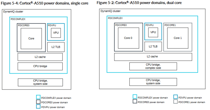
The resulting Cortex A510 introduces a pile of changes. It breaks the 2-wide in-order formula by going 3-wide, but stays in-order. Two A510 cores can be clustered and share a L2 cache, FPU, and L2 TLB. Arm calls this a merged core configuration, and hopes it’ll increase area efficiency with minimal performance impact. Qualcomm has chosen the merged core option in their Snapdragon 8+ Gen 1, and I’ll be using that to test the A510.
High Level
Cortex A510 is a 3-wide in-order core. Cores can be clustered into pairs and share resources to save area, or can be implemented separately. Arm offers a variety of configuration options for core cache sizes and the shared FPU.
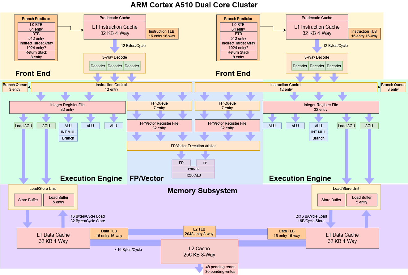
A510 has an eight stage pipeline much like the A55, but the pipeline layout has changed to accommodate the wider decoders. Decoding now takes three pipeline stages instead of one.

However, A510 can redirect the pipeline from the first execution stage if a branch is mispredicted, while A55 could not do so until the writeback stage. Therefore, both cores have a minimum 8 cycle mispredict penalty.
Frontend: Branch Predictor
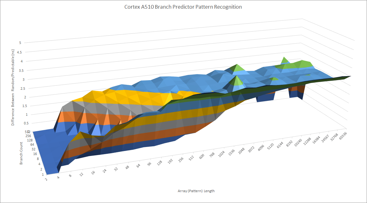
The A510’s branch predictor is an improvement over the A53’s, but is still a basic affair. Qualcomm’s Kryo and Arm’s 7 series cores have predictors capable of recognizing longer patterns, and desktop cores or Arm’s X series take that even further.
To quickly deliver branch targets, Arm has opted for a two level BTB setup. A 64 entry first level BTB can deliver taken branch targets with single cycle latency, while a 512 (?) entry L2 BTB incurs 2 cycle latency. After that, A510 uses a branch address calculator and can handle branches with 4 cycle latency as long as they fit in L1i.

Compared to the Cortex A55, the A510 has twice as much L1 BTB capacity. The A55 likely has no L2 BTB at all, and uses a branch address calculator with 3 cycle latency. A510 will be better for small to moderate branch footprints, but the gap closes as more branches come into play.

Returns are handled by a 8 entry return stack. It’s shallow by big or medium core standards, meaning A510 will struggle with deep calls or crazy recursion. Arm has chosen not to increase the return stack size from A53.
Frontend: Fetch and Decode
Once the branch predictor has provided a fetch target, the frontend looks up the address in the L1 instruction cache (L1i). A510’s L1i is 4-way set associative and can be configured with 32 or 64 KB of capacity. It’s virtually indexed and physically tagged, so lookups to the 16 entry fully associative TLB happen in parallel with cache indexing. The L1i uses a pseudo-random replacement policy, which does away with having to store LRU bits but could decrease hitrate.
Qualcomm has chosen a 32 KB L1i for the Snapdragon 8+ Gen 1’s A510 cores, showing a preference for area density over performance.

A510 can consume an average of 24 bytes per cycle from the L1i, enough to feed the 3-wide decoders. L2 code fetch bandwidth is also improved compared to its predecessor. However, A510 still suffers from poor instruction bandwidth compared to its big-core companions if code spills out to L3.
In a merged core configuration, two A510 cores in the same complex have separate instruction caches and decoders. A cluster can therefore sustian 6 IPC with both cores active as long as code fits within L1i. Once code footprint exceeds L1i capacity, cores will have to fetch code from L2. The L2 is shared by both cores in a complex.

L2 code bandwidth is lower when testing with both cores in a complex versus testing cores in different complexes. Perhaps there’s contention at the shared L2. Code fetch bandwidth from L3 and beyond remains identical regardless of whether we test cores in the same complex. Throughput is likely limited by how many instruction cache misses each core can track.
Execution Engine
After instructions are decoded, they’re dispatched to the execution engine where they can be issued to one of many execution pipes. Like the A53, the A510 can be thought of as having three dispatch ports able to send instructions to several stacks of execution units. Instructions can co-issue if they’re independent, have their inputs ready, and don’t oversubscribe an execution pipe.
Cortex A510 is not strictly in-order and can handle cache misses without blocking up the pipeline. It evidently has queues capable of tracking a few instructions fetched after a load that missed cache. These can’t be compared to out-of-order CPUs with schedulers and significant capacity to hide cache latency because A510 will quickly hit a situation that forces a stall. However, Cortex A510 is better than the A53. Specifically, the A510 can overlap two cache misses with the following between them:
12 total instructions, up from 8 on the A53
6 FP instructions, up from 4 on the A53. This includes 128-bit vector instructions on the A510 but not on the A53. A53 finds vector operations scary and will stall immediately on encountering one
3 branches, unchanged from A53
5 loads. The A53 would stall on any memory access past a cache miss.
Integer Execution
A510 can triple-issue most common operations, including integer adds, logic operations, compares, and register to register moves. Arm’s optimization manual shows a lot of pipes, but not all of them can be thought of as separate execution ports. For example, not-taken jumps and multiplies can’t be dual issued even though they use the branch and MAC pipes. Both are rarer operations that should not show up often within the same three instruction group, so this isn’t a big deal.

In addition to better integer throughput, the A510 adds execution to support pointer authentication for Armv9.
Floating Point and Vector Execution
Maximizing co-issue opportunities is important for in-order cores because a missed dual issue opportunity means lost throughput that can’t be recovered later on. Contrast that with an out-of-order core where large buffers can smooth out spikes for execution unit demand and sustained averages matter more. In-order CPUs therefore need multiple copies of execution units to make the most of co-issue opportunities. Floating point units stand out because FP operations are less common than integer ones, but FP units are expensive. For example, adding two FP numbers involves shifting the mantissa until the exponents match, adding the mantissas, then normalizing the result. The FPU in Cortex A53 and A55 was powerful for a small core and under-utilized in the vast majority of applications. Even in FP heavy programs it would be under-fed thanks to cache and execution latency, which an in-order core struggles to hide.

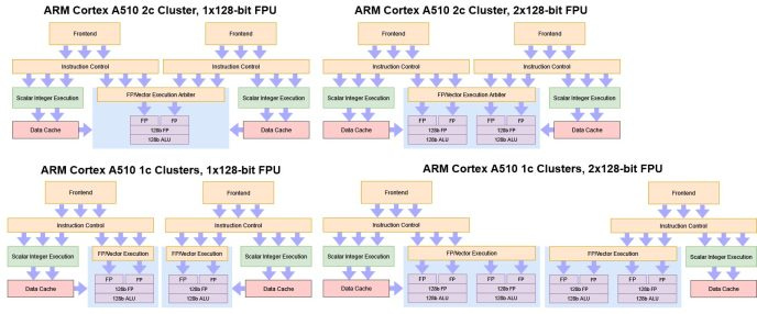
Arm decided having a small, better utilized FPU was better than replicating a FPU per-core. Implementers can opt to not have a merged core configuration or select a more powerful 2×128-bit FPU in the unlikely event that they want high vector performance with low performance cores. In all cases, the FPU sits on a shared power domain and can be powered off independently. Applications that don’t touch the floating point or vector units may be able to run at lower power with the FPU turned off. However, voltage and clock controls don’t get as much flexibility. The entire cluster sits on a single clock and voltage domain.
For the Snapdragon 8+ Gen 1, Qualcomm chose a 2×64-bit shared FPU for maximum area efficiency. A single core can execute two scalar FP operations per cycle, or one 128-bit vector operation. Crypto operations like AES instructions use the same 2×64-bit/128-bit pipe, so an A510 core pair can’t achieve more than 128 bits worth of vector or FP throughput per cycle.

For basic floating point and vector operations, A510’s FPU provides similar throughput to Cortex A55’s. Latency sometimes regresses but remains acceptable. Interestingly, hitting both cores in a complex with FP latency bound tests results in higher observed execution latency. Maybe operations can get unlucky with arbitration logic even when the FP pipes aren’t being saturated.
Cortex A510’s FPU has a PALU pipe for SVE predicate operations that’s not shared even in a merged core configuration. Preventing contention for predicate operations should help keep the FPU fed in SVE workloads by reducing how often vector operations get held up waiting for predicate register dependencies. However, I can’t test this because SVE is not supported on the Snapdragon 8+ Gen 1.
Load/Store
Memory accesses are handled by a pair of address generation pipes. Both can handle loads, and one can handle stores. Indexed addressing requires an additional cycle, giving 4 cycle L1D latency for indexed loads and 3 cycle latency for simple ones. Generated virtual addresses are translated into physical ones by a small 16 entry, fully associative data TLB. A510’s TLBs can handle 40-bit physical addresses, letting the core address 64 GB of physical memory.
For a dual-core configuration sets 0x000-0x0FF access the main TLB and sets 0x100-0x147 access the TLB for IPA and walk entries.
Cortex A510 Technical Reference Manual
Data TLB misses are handled by a 8-way set associative L2 TLB, which is shared by two cores in a complex. Arm didn’t directly specify the entry count but hints that it has up to 2048 entries. The technical reference manual says eight bits are used to index into the main TLB (L2 TLB), so there are 256 sets. Multiplying that by eight ways gives 2048 entries. A510 thus has twice as much L2 TLB capacity as the prior Cortex A55, which used a 1024 entry 4-way L2 TLB. A L2 TLB hit adds 5 cycles of latency over a dTLB hit from testing, though the TRM suggests the penalty should be just three cycles.
Sharing the L2 TLB is a complicated choice. In-order CPUs already struggle with latency and any extra latency from page walks will be devastating. However, the L2 TLB is a major area consumer. The 2048 or 3072 entry L2 TLBs on Zen 3 and 4 are visible as huge chunks of SRAM. Arm’s strategy mirrors Bulldozer’s. The L2 TLB can provide a lot of address translation caching capacity for single threaded loads while maintaining passable capacity for multithreaded ones. At best, a thread gets 8 MB of TLB coverage. At worst, it hopefully gets 1024 entries on average, matching the Cortex A55. Cortex A510’s shared L2 TLB thus help increase utilization for an area-hungry shared resource, but sharing the L2 TLB will probably hurt multithreaded performance more than sharing the FPU.
Cache Alignment and Store Forwarding
Alongside address translation, the load/store unit has to handle memory dependencies. Unlike Arm’s higher performance cores, A510 doesn’t suffer any failed store forwarding penalties. Even partial load/store overlaps are handled with 4 cycle latency. Misaligned accesses can increase latency to 7-8 cycles. A510 is likely taking advantage of its short pipeline and blocking dependent loads until prior stores commit, avoiding a complex store forwarding mechanism.
A510’s data cache has 32 byte alignment for loads and 16 byte alignment for stores. Accesses that cross an alignment boundary see reduced performance because the load/store unit has to make two accesses under the hood. Cortex A55 had 8 byte load alignment and 16 byte store alignment, and therefore could suffer more from misaligned loads.

Vector memory accesses have similar behavior but are more prone to misaligned access penalties. Stores must be perfectly 16B aligned for maximum write bandwidth.
Cache and Memory Access
The L1 data cache is the first stop for memory accesses. Cortex A510 can be configured with either a 32 KB or 64 KB data cache. Both options are 4-way set associative and VIPT. A pseudo-random replacement policy reduces metadata storage requirements in exchange for slightly lower hitrate. Because the data cache can hold the only copy of up-to-date data, it has ECC protection.
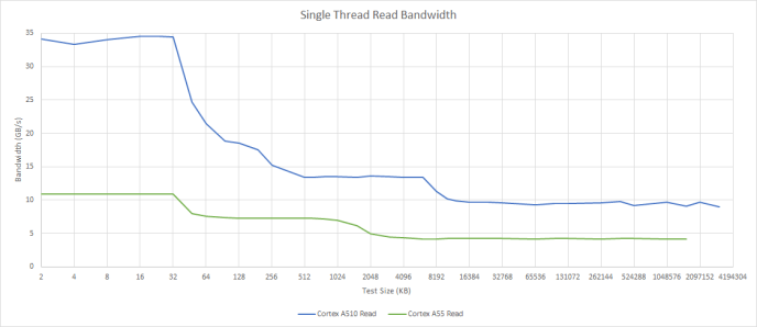
Compared to the Cortex A55, A510 has a massive bandwidth advantage thanks to native 128-bit memory accesses. Unlike Bulldozer, L1D bandwidth scales linearly when testing both cores in a cluster. Each A510 therefore has private 128-bit datapaths between its load/store unit and vector register file.
Past L1D, A510 continues to enjoy more bandwidth from L2, L3, and memory. While a small core like the A510 probably won’t use much bandwidth on average, the improvements should help simple memcpy/memset routines.

Cortex A510’s L2 cache is optional. If implemented, the L2 is 8-way set associative and can have capacities from 128 to 512 KB. Qualcomm seems to use a 128 KB L2 for the Snapdragon 8+ Gen 1’s A510 cores. L2 ECC protection is optional, letting implementers sacrifice reliability for slight area savings. The L2 is shared between two cores in a cluster, as is the off-cluster CPU bridge.

If both cores in a cluster are hammering the L2, bandwidth doesn’t scale well. A510’s cluster behavior is again the opposite of Bulldozer’s, where the L2 provided a lot more bandwidth with both threads in a module active. Past L2, dual core bandwidth can also be constrained by the CPU bridge. Two cores in a cluster can’t pull more L3 bandwidth than one. Strangely, the situation reverses in DRAM where two cores in a cluster can get more bandwidth than one alone.
Latency
Cortex A510 has similar L1 and L2 latency to the Cortex A55. L1 accesses complete in four cycles for simple addressing or 5 cycles for complex addressing. L2 latency is somewhere between 9 to 13 cycles. L2 TLB penalties appear very quickly with 4K pages because the L1 dTLB only has 16 entries.

Past L2, latency is dependent on the SoC implementation. The Snapdragon 8+ Gen 1 has a 6 MB L3 cache, while the Snapdragon 670 has a smaller but faster 1 MB L3. DRAM latency is abysmal, as is typical for mobile chips. We’re looking at 4K pages because Android doesn’t support testing with large pages, but results are horrible even with page walk latency in mind. Over 300 ns of memory latency is crazy. Some GPUs can get data from VRAM faster than that.
Clock Behavior
On the Snapdragon 8+ Gen 1, lscpu says the Cortex A510 cores clock between 307 and 2016 MHz. Much like its Cortex A710 and X2 siblings, A510 can never reach the maximum clock set by Qualcomm.

Clock speeds max out at 1.8 GHz under short or sustained load, so the Snapdragon 8+ Gen 1’s A510 cores run at similar clocks to the Snapdragon 670’s A55 cores (1.7 GHz).
A510 idles at around 0.56 GHz, and boosts to 1.8 GHz in just under 16 ms.

Cortex A510 is therefore the fastest boosting core on the Snapdragon 8+ Gen 1, if only because it maxes out at the lowest clock speeds and requires the lowest power increase to get there.
Final Words
Cortex A510 shakes up Arm’s 5-series lineup. Increasing transistor budgets on better process nodes enable more aggressive designs, and that trickles down to Arm’s 5-series line. Cortex A510 breaks the two-wide, in-order trend that has characterized Arm’s “little” cores for more than a decade. Alongside the core width increase, branch prediction, cache bandwidth, and nonblocking load capability get incremental improvements. Shared resources help improve area efficiency because SoC makers love spamming them.
Shared Resources
Arm has done an excellent job for their first shot at shared resources. A53 and A55 had underutilized dual-issue FPUs.They average less than 1 IPC on code that would be mid-to-high IPC on high performance CPUs. Even FP heavy code needs plenty of scalar integer instructions for control flow and address generation, so A55 and A53’s FP pipes were mostly sitting idle. The L2 TLB is more complicated because in-order cores suffer heavily from cache and memory latency. But if the alternative was two private 1024 entry L2 TLBs like Cortex A55, a large shared 2048 entry one is better. It’ll improve address translation caching capacity for a single thread, while not being worse than A55 for multithreaded loads if Arm does QoS properly.
Then, we have the shared L2 cache and CPU bridge. Arm has used shared L2 caches before with Cortex A72 so sharing these resources isn’t new. Bandwidth never scaled well when all cores in a complex were loaded up. A510 is no different. Beefing up the L2 cache or CPU bridge doesn’t make sense because in-order cores stall so often on memory latency that they won’t make good use of bandwidth.
Implementing shared resources shows Arm’s willingness to take risky moves. While the company’s 7 and X series Cortex architectures see the biggest engineering challenges, the 5 series is not left out of the fun. Multithreaded components present tuning and validation challenges. Arbitration has to avoid starving either thread under heavy load, and power management has to account for whether both cores are active. A core can only tell the shared FPU to power off if the other core is also off, a check that’s unnecessary with single core clusters.
None of this is easy, but difficulty makes for a good learning experience. That sort of experience should give Arm’s little core team the confidence to pull off more complicated things in the future.
Note on Bulldozer
Bulldozer is an obvious comparison because it also shares substantial resources between core pairs. However, shared resources had little to do with Bulldozer’s performance problems. In fact, Bulldozer was most competitive in multithreaded applications where there could be contention for shared resources. Bulldozer issues came from having less per-thread reordering capacity and higher cache latency than Sandy Bridge in a market where single-thread performance was of paramount importance. Cortex A510 does not target the high performance market. If performance did matter A510 would be held back by its in-order execution scheme, not shared resources. Instead of performance, A510 targets low power and area. Sharing resources fits that goal perfectly.
Going Forward
Cortex A510 shows Arm today has more risk appetite and drive to improve their little cores. That’s impressive because the company is maintaining many concurrent CPU lines ranging from the embedded Cortex M to the high performance Cortex X, and they still found engineering resources to do complicated things with their 5-series line.
These engineering investments lay the groundwork for future 5-series cores. Shared resources are great for area efficiency and are here to stay. Its success has been shown with Qualcomm using the merged core configuration in the Snapdragon 8+ Gen 1. Perhaps we’ll see Arm share more resources between core pairs in the future. A shared integer multiplier and divider might work. Maybe there’s room for an even more aggressive approach. I wouldn’t mind if resource intensive web page ads get slammed onto a 8-way clustered little core.
A510’s 3-wide in-order execution scheme is more suspect though. Cortex A53 averaged well under 1 IPC in anything but the most trivial tasks. A510 offers better nonblocking load capability, but bigger buffers will only go so far because in-order cores will be limited by the distance between a cache miss and the first instruction that consumes its data. At some point, an out-of-order core might be more performant and more area efficient. I wonder when or if Arm’s little cores will reach that point.
A510 will likely serve across several generations of big cores as A53 and A55 did, but I look forward to see what Arm does with A510’s successor. Little cores have been a little boring for too many years, and it’s great to see the landscape changing.
If you like our articles and journalism, and you want to support us in our endeavors, then consider heading over to our Patreon or our PayPal if you want to toss a few bucks our way. If you would like to talk with the Chips and Cheese staff and the people behind the scenes, then consider joining our Discord.
On the Dimensity 9000+ the A510 is in the 2-cluster, 2x128B per cluster config.