
Bulldozer, AMD’s Crash Modernization: Caching and Conclusion

In Part 1, we looked at Bulldozer’s core architecture. But the architecture itself isn’t the full story. Memory advances have not kept up with CPU speed, so modern CPUs cope with increasingly sophisticated caching setups. They have to cope with cache latency as well, because high memory latency drives larger caches, and it’s hard to make a cache both large and fast.
To avoid memory bottlenecks, Bulldozer uses a triple level cache hierarchy like many other modern CPUs.
Cache and Memory Access
Bulldozer makes large cache hierarchy changes compared to K10. Latencies are generally higher, but Bulldozer does have a massive amount of on-chip cache.

L1 Data Cache
AMD initially wanted to implement a 64 KB data cache just like the one in K10. But that wouldn’t fit, and ended up sticking out of the module’s sides when they tried. L1D size wound up getting cut to 16 KB, and 3 cycle latency was dropped in favor of making it 4 cycles. Even with a 16 KB cache, AMD had to make concessions to hit their clock speed targets. From AMD’s ISSCC presentation, Bulldozer’s L1D switched to using 8T, 0.294 μm2 bitcells, compared to the 6T ones used in 45 nm K10. 8T means that eight transistors are used to store every bit, reducing storage density. But AMD needed 8T bitcells to improve performance at lower voltages, increase clocks, and reduce power usage. This switch is an example of why transistor density is a poor metric. 8T SRAM would result in higher transistor counts and possibly higher transistor density, but less efficient use of die area. These issues seem related to teething issues on the 32 nm process, because AMD had to use 8T SRAM for Llano’s L1D caches when they shrank K10 to 32 nm. Like Llano, Bulldozer’s L1D uses eight bitcells per bitline. In fairness, most modern designs also use 8T SRAM for the first level caches, so the switch is at least partially due to the challenges of moving to denser nodes.
To cope with the capacity reduction, AMD increased the L1D’s associativity to 4-way. That’s unlikely to make up for the massive capacity decrease, but it’s better than nothing. Smaller capacity also affected the banking scheme, because building a L1D with fewer banks would probably lead to more bank conflicts. K10 and Bulldozer both use banking to let the L1D handle two simultaneous accesses per cycle. To avoid ending up with fewer banks and more bank conflicts, Bulldozer uses a micro-banking scheme to create 16 logical banks within the L1D, similar to K10’s 16 banks.
AMD also took measures to save power. Bulldozer can use a single L1D read to service both L1D ports, if both accesses read the same 16 byte sector. The TLB can also avoid redundant reads if accesses hit the same page, which also happens quite often. 4-way associativity means that 4 tags have to be checked, but AMD uses way-prediction to guess which L1D way will have the requested data. By doing so, it avoids checking four full tags with each access. Bulldozer therefore has a very advanced L1D design, but that’s overshadowed by failing on the fundamentals. The cache simply doesn’t have enough capacity, and hitrate suffers as a result. In some cases, Bulldozer can suffer more than twice as many L1D misses per instruction.

In terms of read bandwidth, the L1D at least maintains performance parity with K10. The cache can service two 128-bit loads per cycle. In theory, each module has two independent L1D caches. However, the FPU can only accept a pair of loads per cycle, and therefore caps a module’s maximum load bandwidth at 2×128-bit.
Unlike read bandwidth, write bandwidth is rather poor because AMD made the L1D write-through.
Write-Through L1D, and WCC
Previously on Chips and Cheese, we compared Netburst’s write through L1D to skydiving without a parachute. In the same way that skydiving setup is easier if you don’t have to care about a parachute, a write-through L1D is easier to implement because the cache never has to hold the only copy of a modified line. That means CPU designers can opt for cheaper parity protection instead of ECC, and don’t have to worry about doing write-backs later. While exhaustive double-blinded studies were not carried out on a large scale, it’s generally accepted that skydiving without a parachute could lead to non-ideal health outcomes. Similarly, Intel learned that a write-through L1D was non-ideal for performance, and didn’t do it again.
AMD’s engineers aren’t stupid, and learned from Intel’s mistake. Instead of writing through to a slow-as-shit L2, Bulldozer’s L1D is write-through to a 4 KB “Write Coalescing Cache” (WCC). The WCC is 4-way set associative, and acts as a write-back cache between the core and L2. Instead of skydiving without a parachute, you can think of this as skydiving with a very small parachute. You might break both legs and various other body parts. But medical literature suggests that waking up in the hospital is an improvement over not waking up at all.

However, the WCC isn’t great. Write bandwidth to it ends up being very mediocre at just over 10 bytes per cycle. Phenom and Sandy Bridge can both sustain a 16 bytes store every cycle, limited by the single write port on their caches. Capacity is also an issue. 4K is not a lot of capacity, especially when it’s shared by two threads. After WCC capacity is exceeded, L2 bandwidth is quite low at just over 5 bytes per cycle on average. Running two threads in the module does not improve write bandwidth.
Bulldozer’s L1D ends up being a significant weak point in the design. Dropping to 4 cycle latency makes the L1D slower than the one in Phenom even if we account for clock speed increases. At the same time, the dramatic reduction in capacity means the core will run into L2 latency more, and have higher demands for L2 bandwidth.
L2 Cache
Bulldozer’s 2 MB, 16-way L2 cache is physically implemented with 0.258 μm2 6T SRAM bitcells. Compared to the 0.275 μm2 6T SRAM bitcells used in Westmere’s L2 cache3, AMD’s bitcells are actually a bit denser. These are arranged into 128 KB slices, each with eight 16 KB macros. The slices are then arranged into four banks. Internally, the L2 cache has a 6 cycle pipeline. We measured 20 cycles of load-to-use latency, which is 16 cycles beyond the 4-cycle L1D. Thinking about the other 10 cycles is a fun exercise. I’m guessing a lot of those are used for queuing and transit.
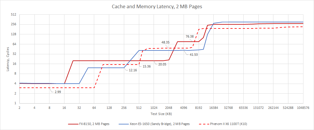
Compared to K10, Bulldozer’s L2 is larger but slower. This is a pretty reasonable tradeoff, because hitrate with a 2 MB cache should be very high. Sandy Bridge’s L2 takes the opposite approach, offering very low latency but only 256 KB of capacity.
In terms of bandwidth, Bulldozer’s L2 is a notable improvement over K10. A single thread gets slightly better bandwidth per clock, and a clock speed bump gives the FX-8150 a 34% L2 bandwidth advantage over the Phenom X6 1100T. Sandy Bridge’s L2 can give a single thread even higher bandwidth, but is much smaller.

When running two threads in the module, Bulldozer can provide twice as much L2 bandwidth. That suggests the L2 has separate paths to each thread’s load/store unit, and lines up with AMD’s publications.

The L2 can thus provide more bandwidth than Sandy Bridge’s, while being eight times larger. I’m a bit sad that the L2 can’t deliver 32 bytes per cycle to a single thread, but perhaps that was an easier way to provide high L2 bandwidth for a multithreaded load. To AMD’s credit, Bulldozer’s L2 does provide an impressive combination of caching capacity and bandwidth, especially if each module is working on a private set of data.

Bulldozer’s L2 is something of a bright point in the architecture. Its size advantage can’t be understated, and will dramatically reduce traffic on the chip’s interconnect. Keeping traffic within the module and off of the L3 is important, because memory performance goes off a cliff after a L2 miss.
L3 Cache, and Interconnect
Bulldozer implements a 8 MB, 64-way set associative L3 cache shared by all cores on the die. While the L3 is large, 8 MB matches the sum of all L2 capacities on the die. To make the L3 effective, AMD tries to make the L3 mostly exclusive of the module-private caches. Specifically, data is removed from the L3 whenever a module brings it into its private caches, unless the data is possibly accessed by multiple modules. The L3 also functions as a victim cache, which means the only way for data to get into the L3 is by getting kicked out of L2.
L3 latency is horrible at over 18 ns. That’s massively higher than Sandy Bridge EP’s 12.7 ns L3 latency. Bulldozer manages to regress compared to Phenom, even compared to Phenom SKUs with lower Northbridge clocks than the FX-8150. For example the Phenom X4 945 has a 2 GHz Northbridge clock, and has 16.35 ns L3 latency. L3 associativity is a distinct culprit here.

From Phenom II to Bulldozer, AMD increased L3 cache capacity to 8 MB by keeping the same number of sets and increasing associativity from 48-way to 64-way. 64-way associativity means that any location in memory can go into 64 possible slots in the cache. Higher associativity reduces the chance of useful lines getting kicked out because of restrictions on where certain memory locations can be cached (conflict misses). But the downside is each way has to be checked to determine if there’s a hit. Doing 64 tag and state checks does not sound cheap at all. I suspect AMD had to lengthen the L3 pipeline to make that happen, increasing latency. But there’s more to the latency story. As the graph above shows, AMD suffered from relatively high L3 latency across Phenom and Bulldozer.
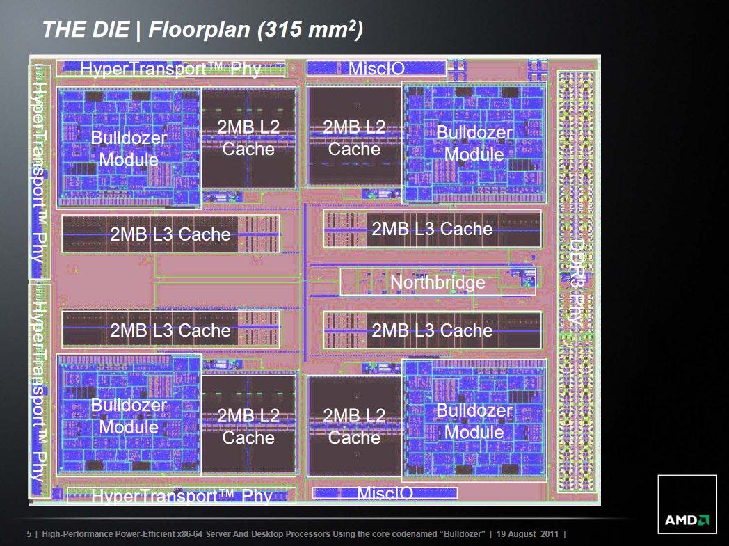
AMD’s Northbridge architecture deserves some discussion here. The Northbridge is AMD’s equivalent of Intel’s “Uncore”, and traces its ancestry back to K8. In K8, more commonly known as Athlon 64, the Northbridge focused on integrating the memory controller onto the die, and enabling more efficient cross-socket connectivity. At this point, the Northbridge’s latency and bandwidth capabilities weren’t too important. DRAM bandwidth would be measured in the low tens of GB/s. IO and cross-socket bandwidth would be lower, and core-to-core traffic would be lower still. And latency for all of those would be very high relative to cache bandwidth.
K10 changes things by adding a L3 cache connected to the Northbridge. Because the Northbridge acted as a central hub between all of the cores, it was a natural place to connect a shared cache. But a cache obviously has much lower latency and higher bandwidth than DRAM. Suddenly, the Northbridge had a lot more to deal with, even though its architecture was mostly unchanged. It ran at much lower clocks than the CPU cores, and tried to handle requests from all CPU cores through a centralized queue.
Bulldozer keeps the same Northbridge architecture. While the L3 looks physically split into four 2 MB sections, all of it has to be accessed behind the centralized Northbridge. In Sandy Bridge, the L3 slices are placed on a ring interconnect, with cache controllers on each ring stop. Intel’s L3 therefore acts a multi-ported, banked cache capable of handling multiple accesses per cycle, and gives Sandy Bridge a massive bandwidth advantage.

But in fairness to AMD, they weren’t alone in trying to stick a L3 behind a centralized crossbar. Intel did the same with Nehalem. We tested Intel’s Xeon X5650, which is a die shrink of Nehalem to Intel’s 32 nm process. L3 latency isn’t great at over 15 ns, but bandwidth is not as horrible as Bulldozer’s. Northbridge or Uncore clock is certainly a variable. Westmere’s Uncore clock is unknown, but it’s unlikely to be more than twice as high as the FX-8150’s 2.2 GHz Northbridge clock.
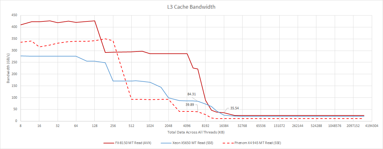
Instead, I think Bulldozer’s victim cache operation is responsible for its read bandwidth deficit. The L3 is only filled by L2 evictions, which means those lines are always written back to L3, regardless of whether they were modified. That can double cache traffic, because the L3 is usually handling a writeback from L2 along with a lookup request. In contrast, Intel’s L3 only receives a victim line if the core wrote to it.
Therefore, when the read bandwidth test sees 35 GB/s on Bulldozer, the L3 is actually dealing with 70 GB/s of bandwidth. If we track L3 hits with performance counters, we see about 35 GB/s. If we include counts from Northbridge event 0x4E2, which tracks L3 fills caused by L2 evictions, we get double that. We can see the full 70 GB/s from software if we use a read-modify-write pattern, in which case the writebacks (copy backs?) are useful to software. But such patterns seem to be more the exception than the rule in practice.
That puts Bulldozer’s L3 bandwidth in a very bad position. A single module on the FX-8150 can pull around 15 GB/s from L3. Running two threads in the module slightly increases bandwidth, but not by much. It’s a slight improvement over the Phenom X6 1100T, where one core can pull 12-14 GB/s from L3, but miles away from Sandy Bridge. The L3 looks even worse when we consider how close it is to DRAM bandwidth. A single module can pull about 12.3 GB/s from DRAM with both threads loaded, or 8.8 GB/s with a single thread. The FX-8150’s L3 therefore beats DRAM bandwidth by less than a factor of two for a single thread, and an embarrassing 25% when a module is running two threads. Sandy Bridge’s L3 is on a different planet.
L3 bandwidth is even more important for multithreaded applications. With all threads active, each module gets under 10 GB/s of bandwidth from L3. That’s less bandwidth than it can pull from DRAM, provided no other modules are active. For sure, having a L3 is still better than nothing, because 35-39 GB/s from L3 is still better than DRAM bandwidth. But Sandy Bridge’s full speed, ring based L3 can give over 30 GB/s to a single core under an all-core load.
Overclocking the Northbridge to 2.4 GHz gives 42 GB/s of L3 bandwidth and 17.2 ns of latency. Maybe we’d see passable L3 performance if the Northbridge clock much higher and run close to core clocks. But attempting to run the Northbridge at even 2.6 GHz resulted in the system locking up, so it’s clear the Northbridge wasn’t designed to run at high clock rates.
The L3 on Bulldozer is a disappointment. It inherits most of K10’s L3 architecture, but regresses performance in return for a minor capacity increase. That regression is unacceptable because K10’s L3 performance was already marginal, and Bulldozer’s increased multithreaded performance means more potential demand for L3 bandwidth. And worst of all, Sandy Bridge is sitting around with an excellent L3 implementation. Bulldozer’s L3 is better than nothing at all, but it’s completely unsuited for its purpose. The L3’s poor performance then dictates a large L2, and it’s hard to make a L2 that’s both large and fast.
Core to Core Coherency Latency
We didn’t cover core to core latency a lot, because cross-core communication is quite rare, and usually not worth spending article space on. But how much something matters depends on both how often it happens, and how expensive it is when it does happen. Bulldozer really pushes the second part of that equation.

Contested lock cmpxchg latency is fine between two threads in a module, but going between modules costs over 200 ns. On average, you’d see about 220 ns of latency for going between threads, assuming the OS isn’t smart enough to schedule threads onto the same module if they communicate with each other a lot. That’s a large regression compared to K10, and also compares badly against Intel’s Sandy Bridge.

Per instruction, core to core latency cost is probably around probably around 10-15% of DRAM latency’s cost, if we compute using figures from the i5-6600K. The i5-6600K’s caching capacity is much lower than Bulldozer’s, so Bulldozer will probably suffer a bit less from L3 misses, bringing that number up a bit. If I had to guess, core to core latency probably docks gaming performance by a percent or so. It’s not a huge issue, but is potentially enough to be slightly more than a rounding error in specific cases.
Memory Controller Performance
In DRAM sized regions, Bulldozer enjoys a traditional AMD advantage with a very low latency memory controller. Compared to Phenom, Bulldozer gains official support for faster DDR3-1866. The test system was set up with relatively fast DDR3-1866 CL10, and we see just 65 ns of memory latency. The Phenom X6 1100T does slightly better at 57.8 ns using DDR3-1600 CL9, but Phenom doesn’t officially support such fast memory anyway.
In terms of bandwidth, Bulldozer gets 23.95 GB/s, beating the Phenom X6 1100T’s 20.55 GB/s. When equipped with fast DDR3-1866, Bulldozer should also outperform Sandy Bridge chips, which only support DDR3-1333.

We’re not going to read too far into memory performance because we can’t match memory setups, but Bulldozer has a reasonably good memory controller.
Performance with 4 KB Pages
2 MB pages are nice for showing raw cache latency, but most client applications use 4 KB pages. On paper, Bulldozer’s larger 1024 entry L2 TLB should help with effective cache access latencies, compared to K10’s smaller 512 entry one. But Bulldozer’s L2 TLB is extremely slow. We see over 15 cycles of added latency at the 1 MB test size. If we try to isolate TLB latency by looking at latency differences when accessing one element per 4 KB page, we get a 20 cycle delta after going past L1 TLB capacity.
One culprit here is that the L2 TLB is placed outside the load/store unit, in what AMD calls the “cache unit” (CU). The CU also contains the L2 cache datapath, placing it far away from the individual cores. Putting the L2 TLB there lets AMD easily share it across both threads, which makes sense because the L2 TLB is a large structure that’s too expensive to duplicate in each thread’s load/store unit. But taking 20 cycles to hit the L2 TLB is not a good tradeoff.
For comparison, hitting the L2 TLB on Sandy Bridge seems to add around 7 cycles, while K10 impressively only suffers a 2-3 cycle penalty. Bulldozer’s smaller L1 TLB doesn’t help either, because that’ll mean fewer lucky hits as memory footprints reach deep into L2 TLB coverage.

As a result, Bulldozer’s L2 advantage is hampered by virtual to physical address translation latency. At test sizes between 512 KB and 2 MB, Bulldozer’s latency ends up quite close to Sandy Bridge or K10’s, even though Bulldozer is fetching data from L2 while the other architectures are doing so from L3. Even when K10 misses its L2 TLB, it still enjoys a massive L3 cache latency advantage over Bulldozer. I suspect that’s because K10 employs a 24 entry page walk cache, which caches entries in the next paging structure up (page directory in this case). That page walk cache would cover 96 MB, and enable relatively fast page walks over that area. Bulldozer uses the L2 TLB as a page walk cache. I have no clue how the architecture determines whether to fill a direct translation or a higher level one into the L2 TLB. But clearly it’s not working very well, because taking 105 cycles to grab data from L3 is moronic.
Bulldozer’s Struggles (Against Sandy Bridge)
Bulldozer struggled to compete against Sandy Bridge especially in single threaded performance. There’s no single cause for this. Rather, Sandy Bridge’s huge lead comes down to a combination of AMD’s struggles and Intel pulling off some incredible advances with Sandy Bridge.
AMD originally wanted to hold the line with Phenom’s IPC while using clock speed increases to deliver a single threaded performance boost. If AMD managed use K10-sized integer and load/store units, I could see that happening. Bulldozer’s shared frontend and FPU can provide full throughput to a single thread. Both shared units are far more powerful than the ones in K10. Combine that with any improvements at all to the per-thread integer and load/store units, and I could actually see an IPC increase over Phenom. But AMD was aiming too high. In one architecture, they were trying to implement a grab bag of advanced architectural techniques, move to a new process node, and multithread parts of the core.
AMD’s 32nm Issues
Unsurprisingly, AMD was forced to cut back. It’s impossible to talk about the cutbacks without talking about the process node and clock speed goals. The company’s publications drop hints of how hard it was to achieve their goals while moving to the 32 nm process.
The change from a 6T cell in 45nm to 8T in 32nm was required to improve low-voltage margin and read timing and to reduce power. Use of the 8T cell also eliminated a difficult D-cache read-modify-write timing path.
Design Solutions for the Bulldozer 32nm SOI 2-Core Processor Module in a 8-Core CPU, ISSCC 2011
Reading between the lines, AMD is saying they switched to less area efficient 8T SRAM because they could not maintain clock speeds. But even that wasn’t enough. They also had to reduce bitline loading by using 8 cells per bitline instead of 16, like on prior generations. From talking to a former AMD engineer, we know the 64 KB L1D was cut to 32 KB, then to 16 KB. The increased area required by the L1D design tradeoffs could also have contributed to making the L1D a write-through design. AMD needed to save all the area they could, and using parity instead of ECC would require less storage.
In the integer unit, AMD duplicated the register file to increase clock speeds. As we saw from die plots earlier, the replicated register file takes a lot of space – space that could have been used to implement more execution units or more reordering capacity.
To remove critical-path wire delay, the physical register file arrays and address generator (AGEN) incrementor are replicated.
Design Solutions for the Bulldozer 32nm SOI 2-Core Processor Module in an 8-Core CPU, ISSCC 2011
It’s easy to blame aggressive clock targets, but I suspect the process node is more at fault here. AMD actually ported K10 to 32 nm for Llano, and suffered similar difficulties even though Llano didn’t target higher clocks. In fact, Llano wound up suffering from lower clocks than its Phenom predecessors. Llano’s story is one for another day, but AMD again points to 32 nm node challenges in its development:
The conversion to the 32nm high-k metal-gate (HKMG) process presents several challenges not encountered in previous generations. The PMOS drive strength increased significantly relative to NMOS. This forced revision of the keeper design for dynamic nodes and caused unacceptable delay increase in some cases.
An x86-64 Core Implemented in 32nm SOI CMOS, ISSCC 2010
In other words, even porting a 45nm design to 32nm with minimal architectural changes was not straightforward, unless you wanted to let clock speeds drop through the floor and eat a massive overall performance decrease. Even with Llano, AMD spent a lot of effort working around 32nm issues before they could deliver a product with acceptable performance.
Electromigration (EM) remediation is more difficult because the current-carrying limits are less than the scaled values projected by geometric scaling. Careful attention is paid to signals with high activity on minimum-width wires. Techniques to reduce capacitance of such nets and specialized straps are used extensively to divert the current across multiple parallel paths.
An x86-64 Core Implemented in 32nm SOI CMOS, ISSCC 2010
I don’t have an electrical engineering background so I won’t read too much into process node challenges, but from reading AMD’s publications, it’s clear that the 32 nm node presented significant difficulties for the Bulldozer effort.
Not Catching Up Enough
While Bulldozer is significantly more advanced than its K10 predecessor, it still trails Sandy Bridge in some areas. Its branch predictor improves over K10’s, but still can’t match Sandy Bridge’s prediction speed or accuracy. Store forwarding is improved, but Sandy Bridge is able to handle far more forwarding cases without penalty. AMD introduced branch fusion for CMP and TEST instructions, but Intel had been iterating on branch fusion since Core 2, and Sandy Bridge can fuse most ALU instructions with an adjacent branch.
In terms of clock speeds, Bulldozer does clock higher than K10. The FX-8150 could boost up to 4.2 GHz, while Llano’s top SKU only reached 3 GHz on the same 32 nm node. But Sandy Bridge also clocked pretty well, and Bulldozer’s clock speed advantage wound up being pretty small.
In other areas, Bulldozer didn’t improve over K10, but Sandy Bridge made huge leaps. For example, AMD kept the same Northbridge and L3 architecture, while Sandy Bridge brought in new ring interconnect. Poor L3 performance forced a larger L2. But enlarging the L2 also gave it worse latency characteristics, which punished Bulldozer’s small, write-through L1D.
Not Big Enough (Per-Thread)
Regardless of whether you want to see the FX-8150 as an eight core or quad core CPU, it performs more like it has eight small cores than four big ones with SMT. Each Bulldozer thread has full access to a module’s frontend bandwidth and FPU resources, but only half of the module’s reordering capacity. With the exception of the FPU scheduler and register file, all of the key out-of-order execution buffers available to a single Bulldozer thread are smaller than the equivalents in Sandy Bridge.
That by itself isn’t necessarily a huge issue. Zen 4 competes well with Golden Cove despite having smaller OoO buffers, but it does so by having a lower latency cache subsystem. Bulldozer’s cache subsystem is higher latency than Sandy Bridge’s, putting Bulldozer in a poor position. If we combine resources available to both threads in a module, Bulldozer starts looking quite decent. For example, a Bulldozer module running two threads would have 2×128 ROB entries available, while a Sandy Bridge core would partition its 192 entry ROB into a 2×96 configuration. The same applies for other structures. Bulldozer can then bring a large reordering capacity advantage to bear, mitigating its cache latency disadvantage. Memory footprint also tends to increase with more threads in play, and Bulldozer’s large caches can come in handy there. In some cases, Bulldozer can be very competitive in well threaded applications.
Competitive multithreaded performance is good, but a lot of desktop applications are not embarrassingly parallel and that is a huge problem for Bulldozer. Four strong cores will be far easier to utilize than eight weak ones. If those four cores can achieve higher throughput via SMT when given eight threads, that’s great. But performance with fewer threads can’t be compromised for client markets.
New Architecture Hard
From the start, AMD knew power efficiency went hand in hand with targeting high multithreaded performance, so Bulldozer has power saving techniques sprinkled in all over the place. They switched to a PRF-based scheme, optimized the scheduler, and used way-prediction to access the 4-way L1D. Clock gating helped reduce power when various functional units like the FPU were idle. AMD paid a lot of attention to reducing critical path lengths in the layout, and even duplicated the integer register file to put the ALUs and AGUs closer.
On top of that, AMD implemented advanced power management techniques. Like Sandy Bridge, Bulldozer actively monitors power to allow for opportunistic boosting while staying within TDP limits. Neither CPU directly measures power consumption. Instead, various events around the CPU are monitored and fed into a model that predicts power consumption.
But we know that in the end, Bulldozer was less power efficient than Sandy Bridge. One reason is that AMD struggled to optimize power in a design that differed radically from their previous ones.
Generally, CPU power efficiency is achieved through careful analysis of the power consumption of the completed implementation to identify waste and reduction opportunities, which are then implemented in a subsequent version of the core. With a ground-up design such as Bulldozer, this sort of analysis loop was not possible: power efficiency had to be designed simultaneously with convergence on timing and functionality
Bulldozer: An Approach to Multithreaded Compute Performance, IEEE 2011
I suspect this is like software optimization, where you first identify the biggest contributors to runtime before targeting your optimization efforts there. If you don’t do your profiling correctly, you could spend a massive amount of time optimizing a section of code that only accounts for a few percent of runtime. Similarly, if you can’t identify the biggest sources of power waste, you might spend a lot of time optimizing something that doesn’t waste a lot of power in the first place. Of course, the actual picture is likely more complex. AMD’s engineers used “RTL-based clock and flip-flop activity analysis as a proxy for switching power”. Transistors that are switching on and off tend to consume more power, so these simulations gave the engineers an idea of where to optimize at an early stage. As the design progressed, AMD got a better idea of what real power consumption would be, but large changes are harder to make as the design nears completion.

High clock targets made power optimization even harder, especially as getting things to clock up on 32 nm seemed to be very difficult. AMD had to tweak transistors to make the right tradeoffs between leakage (power waste) and delay (ability to reach higher clocks).
Bulldozer’s dramatic single-threaded performance loss to Sandy Bridge therefore can’t be explained by a single factor, or even a small set of factors. Rather, Bulldozer has a long list of weaknesses compared to Sandy Bridge. Execution and reordering resources are lower. Penalties are higher and easier to run into. Power consumption was higher. Each individual Bulldozer disadvantage might not be huge by itself, but they stack on top of each other to put AMD way behind Intel. For example, a combination of lower reordering capacity and higher cache latency means the core will have a more difficult time extracting parallelism around L1 misses. But Bulldozer’s issues weren’t purely due to difficulties faced by AMD. Intel also deserves a lot of credit for the massive progress they made with Sandy Bridge. We’ll cover Sandy Bridge in another article, but Intel was able to successfully integrate a batch of techniques they previously trialed in Netburst and other architectures.
Final Words
Bulldozer uses a giant grab bag of new techniques and technologies. In one new architecture, AMD implemented a far more complex branch predictor, multithreaded the frontend and floating point unit, overhauled the out of order execution engine, added AVX support with FMA, and dropped in a pile of other small improvements for good measure. At the same time, they migrated to a new 32 nm process node that presented significant challenges all by itself.
AMD struggled to pull all of these changes off while optimizing for power consumption, creating some similarities to Netburst. But AMD got Netburst’s advantages too, because Bulldozer seems to be a bit of a proving ground for a pile of new techniques that were later used in Zen. In the same way that Netburst arguably fueled Sandy Bridge’s later success, Bulldozer arguably contributed to Zen’s success.

Zen employed a lot of the technologies that debuted in Bulldozer, but far more successfully. After several generations of 15h struggle, AMD had mastered those new techniques and was able to employ them well in Zen. Zen did provide a combination of decent power efficiency and single threaded performance, while beating Intel in multithreaded performance.
However, a Netburst comparison isn’t completely appropriate, because Bulldozer avoids a lot of Netburst’s worst flaws. While Bulldozer often has higher penalties than Sandy Bridge, they’re nowhere near as extreme or as common as what we saw on Netburst. In some corner cases, like loads crossing a 4K page boundary, Bulldozer completely avoids penalties that pop up on Sandy Bridge. Bulldozer’s performance is therefore not far off what you’d expect based on its reordering capacity and cache setup. In contrast, Netburst brought massive reordering capacity and execution resources, but couldn’t match K8 in performance per clock.
Bulldozer was definitely a painful experience, but it was a necessary one for AMD. Like Intel’s P6 architecture, AMD’s Athlon had served the company for more than a decade but was clearly becoming dated and difficult to evolve. Llano’s clock speed struggles on 32 nm are a very good showcase of this. At the same time, AMD probably understood that beating Intel’s single threaded performance would be out of reach, and decided to compete on multithreaded performance. Bulldozer ultimately aimed too high. But AMD’s engineers should be commended for accomplishing as much as they did in a single generation, even if the sum of the parts didn’t produce an impressive whole.
If you like our articles and journalism and you want to support us in our endeavors then consider heading over to our Patreon or our PayPal if you want to toss a few bucks our way or if you would like to talk with the Chips and Cheese staff and the people behind the scenes then consider joining our Discord.
Footnotes
Test Setup

References
1. Design of the Two-Core x86-64 AMD “Bulldozer” Module in 32 nm SOI CMOS, IEEE Journal of Solid-State Circuits, Vol. 47, No. 1, January 2012
2. Design Solutions for the Bulldozer 32nm SOI 2-Core Processor Module in an 8-Core CPU, ISSCC 2011
3. Westmere: A Family of 32nm IA Processors, ISSCC 2010