
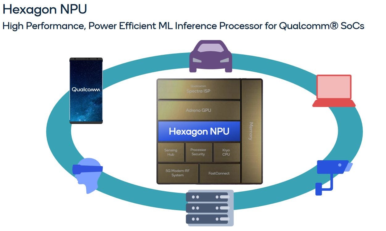
Qualcomm’s Hexagon DSP, and now, NPU

Cell phones have to handle telecommunications and audiovisual processing while maximizing battery life. Digital Signal Processors, or DSPs, use specialized hardware to offload these tasks from the CPU which lowers power usage.
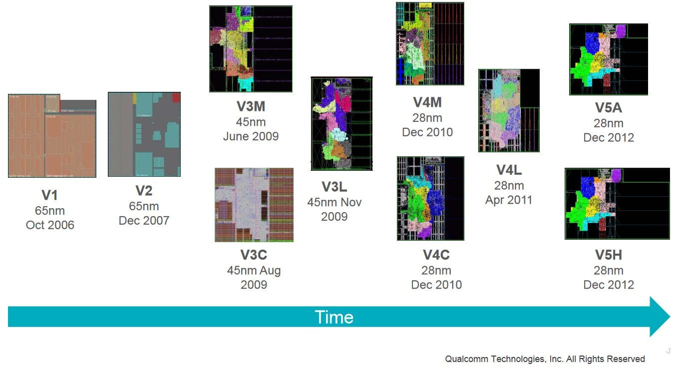
Qualcomm’s Hexagon has a long history of offloading signal processing in the company’s Snapdragon products. To address the recent rise in machine learning applications, Qualcomm is adding matrix multiplication capabilities to Hexagon.
We’d like to thank Qualcomm for putting together a nice Hot Chips presentation on Hexagon. The presentation didn’t go into architectural specifics, so I’ll be filling the gaps from public documentation, assuming missing details from the presentation have remained unchanged.
High Level
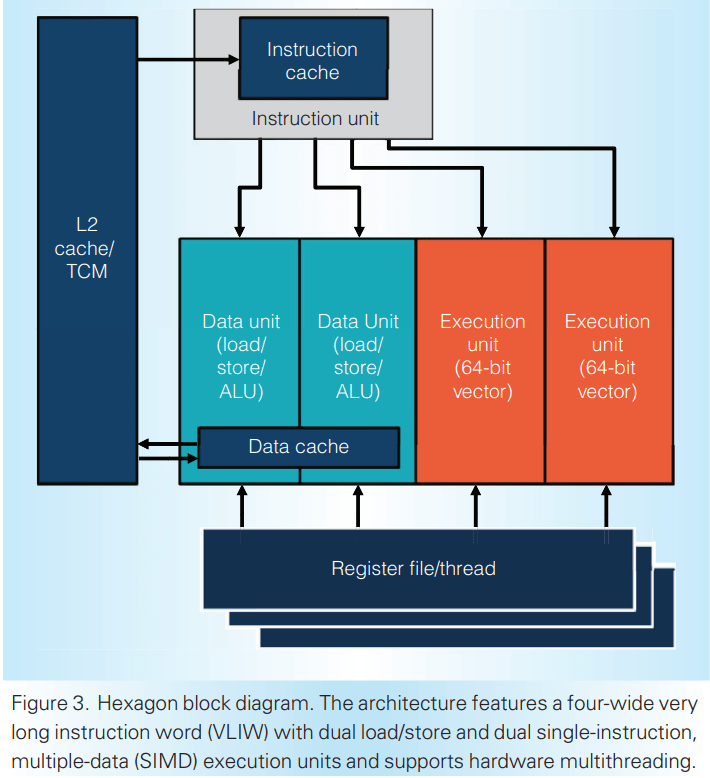
Hexagon is an in-order, four-wide very long instruction word (VLIW) processor with specialized signal processing capabilities. It uses SMT to take advantage of thread-level parallelism and hide latency. Hexagon uses a co-processor model for its vector and tensor units, and is able to provide massive per-clock throughput.

Hexagon supports virtual memory and caching just like a CPU, and can run compiled C code. However, it has a different execution model where instructions are first committed and then executed. This model enables deep execution pipelines, but the drawback is certain exceptions can only be caught after commit and therefore won’t be precise.

In the Snapdragon 8 Gen 2, Hexagon has 6-way SMT. Qualcomm’s DSP thus lands somewhere between GPUs with 12/16 threads per SMSP/SIMD, and CPUs that rarely go beyond 2-way SMT. Each Hexagon thread gets a scalar context by default, but has to request access to use the vector or tensor co-processors.
Frontend
Branch prediction is normally associated with high-performance CPUs. However, Qualcomm has seen fit to implement a branch predictor for Hexagon, as evidenced by performance monitoring events for BTB and return stack hits. Event descriptions suggest most branches can be handled with a two-cycle latency, and less commonly a 3-cycle latency. In the case of 3 cycles, the BTB probably doesn’t have a target cached for the branch, and the decoders calculate the destination address. If so, the instruction cache would have 3-cycle latency.
Direction prediction is likely provided via simple bimodal counters, with a mechanism similar to the original Pentium. Even a simple branch predictor is better than no predictor, allowing Hexagon to perform well without leaning hard on thread-level parallelism.
Fetch and Decode
Once the branch predictor has provided a target address, Hexagon fetches a 128-bit VLIW bundle from the instruction cache. Qualcomm didn’t specify Hexagon’s instruction cache size, but prior versions had 16 KB. I wouldn’t be surprised if Hexagon maintained the same instruction cache size because throughput-bound applications tend to have small instruction footprints.
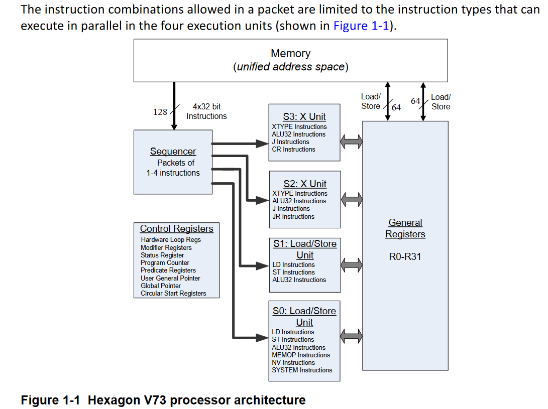
Each VLIW bundle contains up to four instructions, making me wonder why Qualcomm chose the “Hexagon” name. “Qualcomm Quadrilateral” would have made more sense and sounded better. VLIW bundles allow superscalar execution with simple hardware. Decoders are cheap because specific VLIW positions only contain a subset of instructions. Hardware read-after-write and write-after-write hazard resolution is not necessary, because instructions packed into a VLIW bundle have to be independent, and cannot write to the same destination register. Execution pipe selection logic is also simplified, because each VLIW bundle position corresponds to an execution pipe.
After instructions are fetched and decoded, they’re sent to the appropriate unit, or co-processor, for execution.
Scalar Integer Execution
Hexagon has a 32-bit scalar unit with 32 registers per thread context. Unlike the scalar unit on AMD’s GCN or RDNA, which mainly offloads control flow and address generation operations from the vector units, Hexagon’s scalar unit is quite powerful and can handle lightweight DSP tasks on its own. It can complete up to four instructions per cycle thanks to VLIW packing, and each instruction can represent a lot of work. There are specialized instructions for sum of absolute differences (SAD), bitfield manipulation, and context-adaptive binary arithmetic coding (CABAC) for H.264 decode. The “scalar” unit can even do vector operations. Byte or halfword (16-bit) elements can be packed into a 32-bit register. Adjacent 32-bit registers can be addressed as a 64-bit one, allowing longer vector width operations including 2 x 32-bit ones. Two of the scalar unit’s pipes can handle floating point operations too. It’s like Intel’s MMX, except the vector registers are aliased to the general purpose ones.

Hardware loop and circular buffer handling help improve instruction density and register utilization. Two pairs of loop start and loop count registers provide hardware looping support, freeing up general purpose registers to hold other data. Hardware looping can assist the branch predictor, but mispredictions can still occur with small loops with iteration counts of two or less. Circular buffers get hardware support too. The CS0 and CS1 registers store the buffer base, and buffer length is stored in the M0 or M1 registers. A program can then use circular buffers without bounds checking for every pointer increment. A special “global pointer” register can be used with a global pointer relative addressing mode, helping access global or static data. These mechanisms can reduce register pressure.

Scalar-side memory accesses are serviced by a L1 cache of unspecified size, though Hexagon has used a 32 KB L1D in the past. The L1 data cache only has two 64-bit ports and is dedicated to the scalar unit. Hexagon’s load/store unit resolves edge cases like memory dependencies, page crossing, store buffer fills, and cache bank conflicts via replay.
L1 misses are handled by a L2 cache. Again, Qualcomm didn’t give the cache size, but the Snapdragon 820’s Hexagon DSP used a 512 KB L2. The older Snapdragon 800 used a 256 KB L21, so Qualcomm’s current DSPs might have a 1 MB or larger L2. The v73 PRM refers to a L2 scoreboard with 32 entries, so the L2 cache can probably handle 32 pending requests.
Vector Execution (HVX)
Hexagon Vector Extensions, or HVX, provides more grunt for heavier DSP tasks. HVX provides 32 1024-bit vector registers and a set of execution pipes that roughly map to VLIW bundle positions. Hexagon DSPs often have fewer vector contexts available than scalar ones, so threads have to request HVX access. The Hexagon V73 PRM gives an example with four vector contexts. Four contexts would have 16 KB of vector registers. For comparison, Intel’s Skylake-X has 10.7 KB of vector registers for AVX-512 support. Having threads request HVX capability rather than providing it by default lets Hexagon get by without GPU-sized register files, and power down the vector coprocessor for lightweight tasks.

Besides the large vector register file, HVX provides four 128-bit predicate registers per thread. Predicate registers can hold results for vector compares, and can be used as a mask for some instructions like conditional accumulates.
Past Hexagon implementations focused exclusively on vector integer operations, but Qualcomm has added floating point capability to make HVX more flexible.
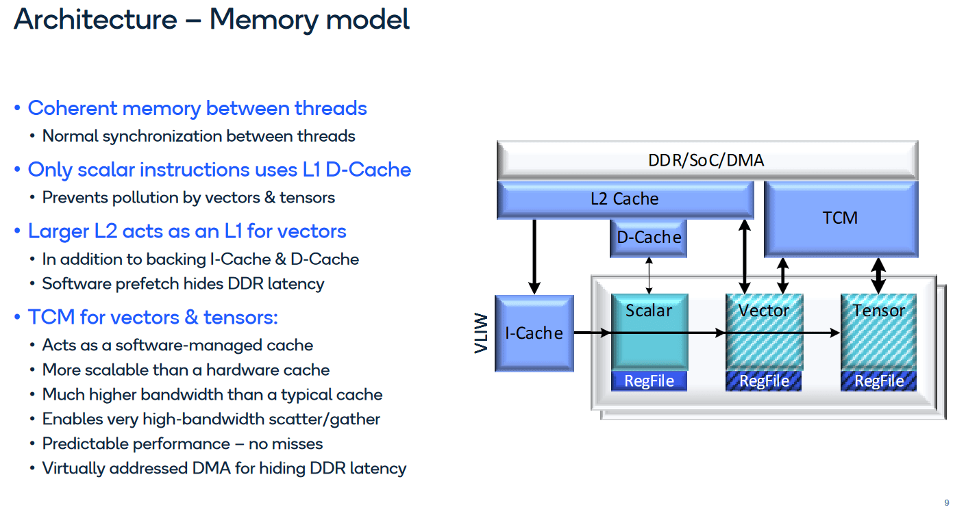
Because vectorized applications tend to have large memory footprints, Qualcomm doesn’t even try to cache vector accesses in L1. Instead, the vector unit uses the L2 cache as its first cache level. Alongside the L2 cache, Hexagon features a large TCM, or Tightly Coupled Memory. This is a software managed scratchpad like AMD GCN’s LDS, but big. Hexagon on Snapdragon 8 Gen 2 has a 8 MB TCM.
The TCM is instrumental to Hexagon’s high performance scatter and gather operations. Gather instructions fill up a vector from non-contiguous locations in memory, and scatters do the same in the opposite direction. Scatters and gathers are difficult for a cache because a 1024-bit vector with 128 byte sized elements could require 128 memory accesses. Looking up a line in a set-associative cache would require comparing an address against every tag in the set. A worst-case gather from a hypothetical 512 KB, 8-way L2 could require 128 * 8 = 1024 tag comparisons. Since the TCM isn’t a cache, it avoids the overhead of tag checks. Hexagon doesn’t even try to do scatter and gather operations on cacheable memory, and only does them on the TCM.
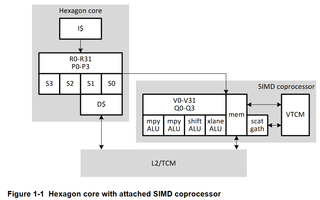
Like the scalar side, HVX has specialized DSP hardware. A histogram instruction helps calculate a 256-bin histogram of brightness values in an image, and consumes all execution resources over four VLIW bundles. Other vector instructions are similar to what you might find on AVX, and include vector adds, min/max, absolute value, and some reduction operations.
Tensor
HVX could do a passable job at multiplying matrices for machine learning, but like Nvidia, AMD, and Intel, Qualcomm saw plenty of optimization opportunities. Specialized matrix multiplication instructions allow more work to be done per instruction, reducing power overhead. Accumulators can get special treatment because values get added to them, but the accumulator values otherwise don’t get read much (other than getting downconverted before being written back out to memory). Qualcomm therefore added a tensor coprocessor to Hexagon. I’m surprised they didn’t call it the “Qualcomm Rectangle” because that’s what matrices look like.
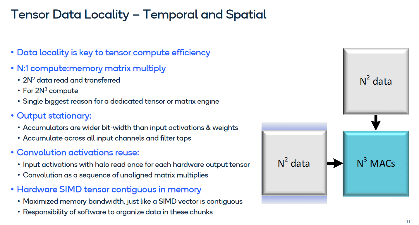
Hexagon’s NPU can complete a massive 16K multiply accumulate operations per cycle, likely using 4-bit weights. For comparison, 16 AIE-ML tiles on AMD Phoenix’s XDNA can complete 8K multiply accumulate ops per cycle with 4-bit integer precision, achieving 20 TOPS at 1.25 GHz. XDNA likely runs at a much higher clock than Hexagon’s NPU. Qualcomm didn’t disclose clock targets, but we can infer that by looking at prior generations.

The Snapdragon 855/865 clocked their Hexagon DSP at 576 MHz. If the DSP can achieve the same clocks with the tensor unit active, it should be capable of 18.8 TOPS, putting it roughly on par with Phoenix. I also wouldn’t be surprised if Hexagon ran at lower clocks under tensor load. But even if that’s the case, Qualcomm is confident their latest DSP can beat their previous ones in machine learning applications.

Final Words
Hexagon provides insight into the strange world of DSPs. It sits between the CPU and GPU worlds, combining wide vector and tensor units with CPU comforts like branch prediction. Thread level parallelism capabilities also land in a middle ground. Hexagon uses 6-way SMT, giving it more thread level parallelism than a typical CPU core. But it lacks the massive register files that GPU execution units use to keep a dozen or more threads in flight. 4-wide VLIW execution also aims for a middle ground. Recent GPUs are basically scalar machines with occasional dual issue capability, while CPUs feature wide out-of-order execution. VLIW isn’t as flexible as out-of-order execution but allows higher per-thread performance for well behaved code.
The resulting processor thus delivers some CPU comforts while still leaning heavily on the instruction set to simplify hardware. It’s likely an ideal combination for lightweight DSP tasks like audio decoding. Those applications should be predictable enough for VLIW to do well and aren’t parallel enough to justify running on a GPU. For a while, a “scalar” unit was all Hexagon needed.
As processing requirements grew, Qualcomm added HVX to increase DSP throughput. Not all DSP tasks would benefit from wide vector execution, so having threads acquire and release the HVX coprocessor made a lot of sense. Qualcomm called out image processing as one of Hexagon’s key applications, and the rise in cell phone camera resolutions likely justified HVX.
Now, machine learning has promoted Qualcomm to add a tensor unit to Hexagon. As with HVX, the tensor unit is a coprocessor that threads must request access to. Qualcomm didn’t provide details on register file sizes, and their Hot Chips presentation focused on the tradeoffs of using different data types. But the addition of a tensor unit shows Hexagon’s extensibility, and Qualcomm’s determination to expand Hexagon’s role.
Qualcomm’s newest Hexagon models thus cover a lot of area. Scalar, vector, and tensor units allow the DSP to handle everything from audio playback to image processing to machine learning. However, tapping into that potential will be difficult.
However, the Hexagon DSPs are notoriously hard to program. While the Snapdragon CPU and GPU can be targeted using OpenMP and OpenCL, respectively, no such model exists for the DSP. Additionally, the DSP is a VLIW processor, and writing efficient code to target this processing paradigm requires architecture specific knowledge of the DSP.
Anthony Cabrera et al, “Toward Performance Portable Programming for Heterogeneous System-On-Chips: Case Study with Qualcomm Snapdragon SoC
Besides not having the software ecosystem a CPU or even GPU would enjoy, Hexagon’s most advanced capabilities require architecture-specific coding. Scatter/gather and tensor compute only access the TCM and can’t operate on global memory. Software has to shoulder a heavy burden and manage data movement between the TCM and memory. Histogram calculations and CABAC decode have specialized instructions, but programmers will have access them via intrinsics or assembly.
But if developers put in the required effort and sanity sacrifice, Hexagon provides high per-clock throughput while avoiding some GPU pitfalls. It could be just the right solution for a lot of cell phone tasks.
If you like our articles and journalism, and you want to support us in our endeavors, then consider heading over to our Patreon or our PayPal if you want to toss a few bucks our way. If you would like to talk with the Chips and Cheese staff and the people behind the scenes, then consider joining our Discord.
References
Martin Saint-Laurent et al, “A 28 nm DSP Powered by an On-Chip LDO for High-Performance and Energy-Efficient Mobile Applications”
Qualcomm Hexagon V73 Programmer’s Reference Manual
Qualcomm Hexagon V73 HVX Programmer’s Reference Manual
Anthony Cabrera et al, “Toward Performance Portable Programming for Heteogeneous System-on-Chips: Case Study with Qualcomm Snapdragon SoC”
Lucian Codrescu et al, “Hexagon DSP: An Architecture Optimized for Mobile Multimedia and Communications”
I have few remarks and questions:
"Gather instructions fill up a vector from non-contiguous locations in memory, and scatters do the same in the opposite direction."
Generally scatter gather is at page granularity (4KB/16KB/64KB). Do you mean that they have a scatter gather at Byte granularity ?
This is what you seem to say in "1024-bit vector with 128 byte sized elements could require 128 memory accesses."