
ARM’s Cortex A53: Tiny But Important

Tech enthusiasts probably know ARM as a company that develops reasonably performant CPU architectures with a focus on power efficiency. Product lines like the Cortex A7xx and Cortex X series use well balanced, moderately sized out-of-order execution engines to achieve those goals. But ARM covers lower power and performance tiers too. Such cores are arguably just as important for the company. The Cortex A53 is a prominent example. Unlike its bigger cousins, A53 focuses on handling tasks that aren’t sensitive to CPU performance while minimizing power and area. It fills an important spot in ARM’s lineup, because not all applications require a lot of processing power.
If I had to guess, cell phone makers shipped more A53 cores than any other ARM core type from 2014 to 2017. As a “little” core in mobile SoC, A53 outlasted two generations of its larger companions. Mobile SoCs often shipped as many “little” cores as “big” ones, if not more. Qualcomm’s Snapdragon 835 used four Cortex A73s as “big” cores, while four A53s were set up as a “little” cluster. Some lower end mobile chips were even fitted out exclusively with A53 cores. For example, the Snapdragon 626 used eight A53 cores clocked at 2.2 GHz.
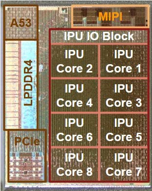
Even after the A55 came out and gradually took over the “little” role in mobile SoCs, A53 continued to appear in new products. Google’s 2018 Pixel Visual Core used an A53 core to manage an array of image processing units. Socionext used 24 A53 cores to create a fanless edge server chip. Beyond that, Roku has used A53 in set-top boxes. A53 made a lot of devices tick, even if it doesn’t dominate spec sheets or get shiny stickers on boxes.
I’m testing the Cortex A53 cores on the Odroid N2+, which uses the Amlogic S922X. The Amlogic S922X is a system-on-chip (SoC) that implements a dual core A53 cluster, a quad core A73 cluster, and a Mali G52 iGPU. Besides the Odroid N2+ single board computer, the S922X also appears on a few set-top boxes. Unlike Intel and AMD, ARM sells their core designs to separate chip designers, who then implement the cores. Therefore, some content in this article will be specific to that implementation.
Architecture
ARM’s Cortex A53 is a dual issue, in-order architecture. It’s a bit like Intel’s original Pentium in that regard, but modern process nodes make a big difference. Higher transistor budgets let A53 dual issue a very wide variety of instructions, including floating point ones. A53 also enjoys higher clock speeds, thanks both to process technology and a longer pipeline. Pentium had a five stage pipeline and stopped at around 300 MHz. A53 clocks beyond 2 GHz, with an eight-stage pipeline. All of that is accomplished with very low power draw.

We’ve analyzed quite a few CPUs on this site, including lower power designs. But all of those are out-of-order designs, which still aim for higher performance points than A53 does. A53 should therefore be an interesting look at how an architecture is optimized for extremely low power and performance targets.
Branch Predictor
A CPU’s pipeline starts at the branch predictor, which tells the rest of CPU where to go. Branch prediction is obviously important for both performance and power, because sending the pipeline down the wrong path will hurt both factors. But a more capable branch predictor will cost more power and area, so designers have to work within limits.
A53 is a particularly interesting case both because it targets very low power and area, and because branch prediction accuracy matters less for it. That’s because A53 can’t speculate as far as out-of-order CPUs. A Zen or Skylake core could throw out over a hundred instructions worth of work after a mispredict. With A53, you can count lost instruction slots with your fingers.
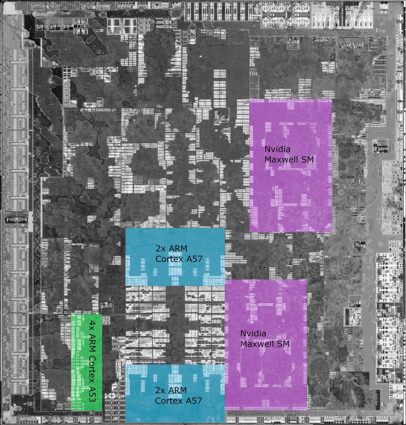
So, ARM has designed a tiny branch predictor that emphasizes low power and area over speed and accuracy. The A53 Technical Reference Manual states that the branch predictor has a global history table with 3072 entries. For comparison, AMD’s Athlon 64 from 2003 had a 16384 entry history table. Qualcomm’s Snapdragon 821 is an interesting comparison here, because it’s contemporary to the A53 but used the same Kryo cores in a big.little setup. Kryo’s branch prediction is much more capable, but Qualcomm’s approach is also quite different because the “little” Kryo cores occupy the same area as the big ones.

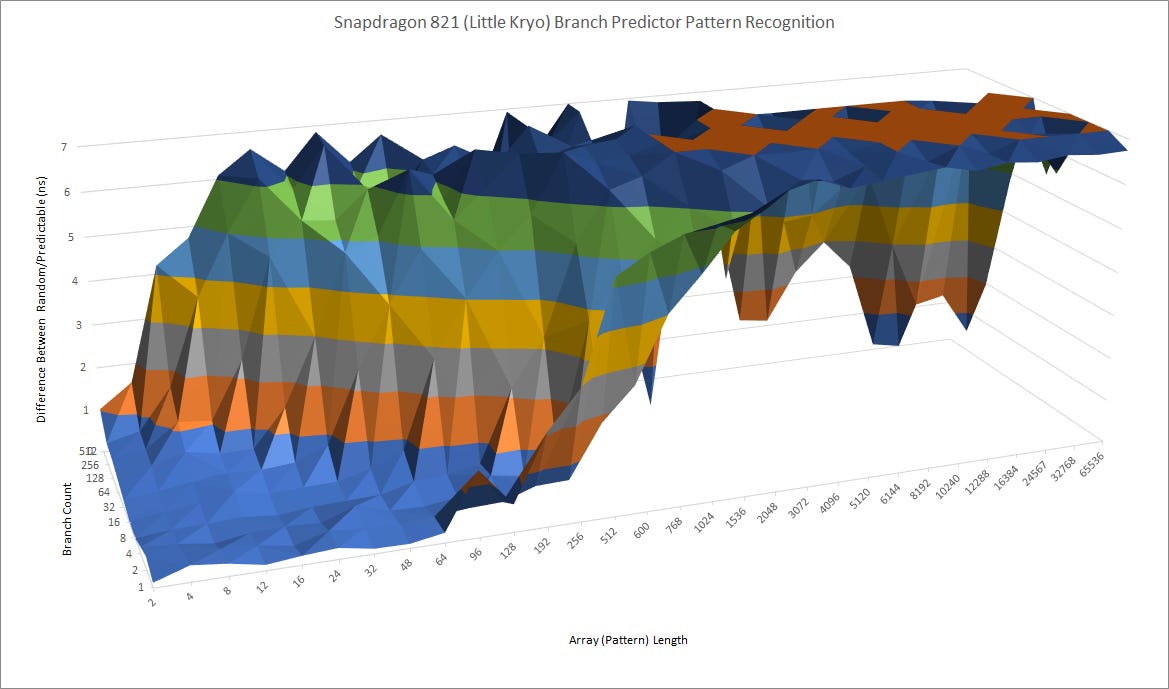
A53 struggles in our testing to recognize a repeating pattern with a period longer than 8 or 12. It also suffers with larger branch footprints, likely because branches start destructively interfering with each other as they clash into the same history table entries.
Return Prediction
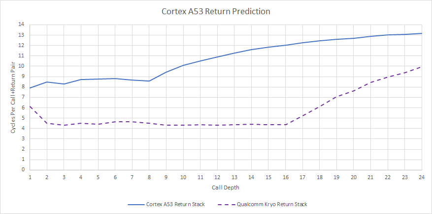
For returns, the A53 has an eight-deep return stack. This is quite shallow compared to other cores. For example, Kryo has a 16-deep return stack. AMD’s Athlon 64’s return stack had 12 entries. But even an eight-deep return stack is better than nothing, and could be adequate for the majority of cases.
Indirect Branch Prediction
Indirect branches can go to multiple targets, adding another level of difficulty to branch prediction. According to ARM’s Technical Reference Manual, the A53 has a 256 entry indirect target array. From testing, the A53 can reliably track two targets per branch for up to 64 branches. If a branch goes to more targets, A53 struggles compared to more sophisticated CPUs.

Again, the A53 turns in an underwhelming performance compared to just about any out-of-order CPU we’ve looked at. But some sort of indirect predictor is better than nothing. Object oriented code is extremely popular these days, and calling a method on an object often involves an indirect call.
Branch Predictor Speed
Branch speed is important too. If the predictor takes a few cycles before it can steer the pipeline, that’s lost frontend bandwidth. A lot of high performance CPUs employ branch target buffers to cache branch targets, but A53 doesn’t do that. Most of the time, it has to fetch the branch from L1i, decode it, and calculate the target before it knows where the branch goes. This process takes three cycles.
For very tiny loops, A53 has a single entry Branch Target Instruction Cache (BTIC) that holds instruction bytes for two fetch windows. I imagine each fetch window is 8 bytes, because that would correspond to two ARM instructions. The BTIC would probably be a 16 byte buffer in the branch predictor. From testing taken branch latency, we do see BTIC benefits fall off once branches are spaced by 16 bytes or more.
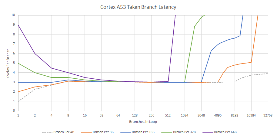
If we do hit the BTIC, we can get two cycle taken branch latency. The “Branch Per 4B” case doesn’t count for ARM because ARM instructions are 4 bytes, and a situation where every instruction is a branch does not make sense. Zooming out though, the BTIC’s effect is quite limited. It’ll only cover extremely tiny loops without any nested branches.
Once branches spill out of the 32 KB L1 instruction cache, latency heads for the hills. Without a decoupled branch target buffer, the A53 won’t know where a branch goes before the branch’s instruction bytes arrive. If those instruction bytes come from L2 or beyond, the frontend would have to stall for a lot of cycles. If we present the data in terms of branch footprint in KB, we can take a glimpse at L2 and memory latency from the instruction side. It’s pretty cool, because normally this kind of test would simply show BTB latency, with the branch predictor running ahead and largely hiding cache latency.

This also means A53 will suffer hard if code spills out of the instruction cache. There’s very basic prefetching capability, but it’s not driven by the branch predictor and struggles to hide latency once you branch over enough instructions.
Instruction Fetch
Once the branch predictor has generated a fetch target, the CPU’s frontend has to fetch the instruction bytes, decode them to figure out what it has to do, and pass the decoded instructions on to the backend.
To accelerate instruction delivery, the S922X’s A53s have 32 KB, 2-way set associative instruction caches. ARM lets chipmakers configure instruction cache capacity between 8 and 64 KB, so the cache could have different sizes on other chips. The instruction cache is virtually indexed and physically addressed, allowing for lower latency because address translation can be done in parallel with cache indexing.
ARM has heavily prioritized power and area savings with measures that we don’t see desktop CPUs from Intel and AMD. Parity protection is optional, allowing implementers to save power and area in exchange for lower reliability. If parity protection is selected, an extra bit is stored for every 31 bits to indicate whether there’s an even or odd number of 1s present. On a mismatch, the cache set with the error gets invalidated, and data is reloaded from L2 or beyond. ARM also saves space by storing as little extra metadata as possible. The L1i uses a pseudo-random replacement policy, unlike the more popular LRU scheme. LRU means the least recently used line in a set gets evicted when a new data is brought into the cache. Implementing a LRU scheme requires storing additional data to track which line was least recently accessed, essentially using extra area and power to improve hitrates.
To further reduce power and frontend latency, the L1i stores instructions in an intermediate format, moving some decode work to predecode stages before the L1i is filled. That lets ARM simplify the main decode stages, at the cost of using more storage per instruction.
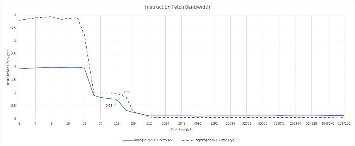
The instruction cache has no problems feeding the two-wide decoders. Qualcomm’s little Kryo has a huge advantage over the A53, because it’s really a big core running at lower clocks with a cut-down L2 cache. Kryo’s frontend can fetch and decode four instructions per cycle, making it quite wide for a low power core in the 2017 timeframe.
However, A53 and Kryo both see a massive drop in instruction throughput when code spills out of the instruction cache. L2 code fetch bandwidth can only sustain 1 IPC on Kryo, and even less on A53. 1 IPC would be four bytes per cycle. ARM’s technical reference manual says the L1i has a 128-bit (16 byte) read interface to L2. The CPU likely has a 128-bit internal interface, but can’t track enough outstanding code fetch requests to saturate that interface. To make things even worse, there’s no L3 cache, and 256 KB of L2 is not a lot of capacity for a last level cache. Instruction throughput is extremely poor when fetching instructions from memory, so both of these low power cores will do poorly with big code footprints.
Execution Engine
Once instructions are brought into the core, they’re sent to the execution engine. Unlike the original Pentium, which had a fairly rigid two-pipe setup, the A53 has two dispatch ports that can flexibly send instructions to several stacks of execution units. Instructions can dual issue as long as dependencies are satisfied and execution units are available. Many execution units have two copies, so dual issue opportunities are likely to be limited by dependencies rather than execution unit throughput.
The execution engine is cleverly designed to get around pipeline hazards that would trip up a basic in-order core. For example, it seems immune to write-after-write hazards. Two instructions that write to the same ISA register can dual issue. I doubt the A53 does true register renaming, which is how out-of-order CPUs get around the problem. Rather, it probably has conflict detection logic that prevents an instruction from writing to a register if it has already been written to by a newer instruction.
Since there’s no register renaming, we also don’t see renamer tricks like move elimination and zeroing idiom recognition. For example, XOR-ing a register with itself, or subtracting a register with itself will have a false dependency on the previous value o the register (even though the result will always be zero).
Integer Execution Units
A53 can dual issue the most common operations like integer adds, register to register MOVs, and bitwise operations. Less common operations like integer multiplies and branches can’t be dual issued, but can issue alongside another type of instruction.
Mixing integer multiplies and branches results in about 0.7 IPC, so the two functional units share a pipe and cannot dual issue. That shouldn’t be a big deal, but it does suggest the A53 organizes the two integer pipes into a basic one and a complex one.
Floating Point and Vector Execution
Unlike the original Pentium, which only had one FP pipe, the A53 uses modern transistor budgets to dual issue common floating point instructions like FP adds and multiplies. That’s a nice capability to have because Javascript’s numbers are all floating point, and A53 may have to deal with a lot of Javascript in phones. Unfortunately, latency is 4 cycles, which isn’t good considering the A53’s low clock speed. It’s even worse because the A53 doesn’t benefit from a big out-of-order engine, which means the core has to stall to resolve execution dependencies.

The same dual issue ability doesn’t apply to vector operations. A53 supports NEON, but can’t dual issue 128-bit instructions. Furthermore, 128-bit instructions can’t issue alongside scalar FP instructions, so a 128-bit operation probably occupies both FP ports regardless of whether it’s operating on FP or integer elements.
Nonblocking Loads
The A53 also has limited reordering capability that gives it some wiggle room around cache misses. Cache misses are the most common long latency instructions, and could easily take dozens to hundreds of cycles depending on whether data comes from L2 or memory. To mitigate that latency, the A53 can move past a cache miss and run ahead for a number of instructions before stalling. That means it has internal buffers that can track state for various types of instructions while they wait to have their results committed.
But unlike an out-of-order CPU, these buffers are very small. They likely consume very little power and area, because they don’t have to check every entry every cycle like a scheduling queue. So, the A53 will very quickly hit a situation that forces it to stall:
Having eight total instructions in flight, including the cache miss
Any instruction that uses the cache miss’s result (no scheduler)
Any memory operation, including stores (no OoO style load/store queues)
Having four floating point instructions in flight, even if they’re independent
Any 128-bit vector instruction (NEON)
More than three branches, taken or not
Because the A53 does in-order execution, a stall stops execution until data comes back from a lower cache level or memory. If a cache miss goes out to DRAM, that can be hundreds of cycles. This sort of nonblocking load capability is really not comparable to even the oldest and most basic out-of-order execution implementations. But it does show A53 has a set of internal buffers aimed at keeping the execution units fed for a short distance after a cache miss. So, A53 is utilizing the transistor budget of newer process nodes to extract more performance without the complexity of out-of-order execution.
Memory Execution
The A53 has a single address generation pipeline for handling memory operations. Assuming a L1D hit, memory loads have a latency of 3 cycles if a simple addressing mode is used, or 4 cycles with scaled, indexed addressing. This single AGU pipeline means the A53 cannot sustain more than one memory operation per cycle. It’s a significant weakness compared to even the weakest out-of-order CPUs, which can usually handle two memory operations per cycle.
Load/Store Unit
A CPU’s load/store unit has a very complex job, especially on out-of-order CPUs where it has to track a lot of memory operations in flight and make them appear to execute in program order. The A53’s load/store unit is simpler thanks to in-order execution, but handling memory operations still isn’t easy. It still has to handle instructions that address memory with byte granularity and varying sizes, with a L1 data cache that accesses a larger, aligned region under the hood. It still has to handle memory dependencies. Even though the A53 is in-order, pipelining means a load can need data from a store that hasn’t committed yet.
The A53 appears to access its data cache in 8 byte (64-bit) aligned chunks. Accesses that span a 8 byte boundary incur a 1 cycle penalty. Forwarding similarly incurs a 1 cycle penalty, but notably, there is no massively higher cost if a load only partially overlaps a store. In the worst case, forwarding costs 6 cycles when the load partially overlaps the store and the load address is higher than the store address.
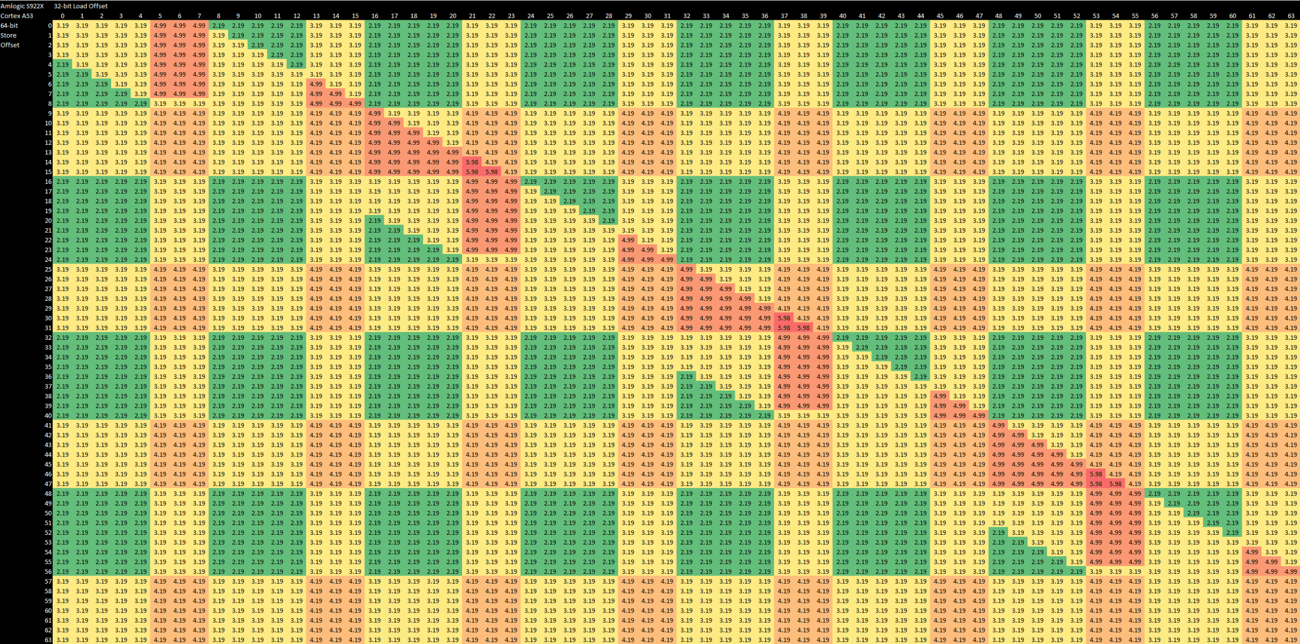
Contrast that with Neoverse N1, which incurs a 10-11 cycle penalty if a load isn’t 4-byte aligned within a store. Or Qualcomm’s Kryo, which takes 12-13 cycles when a load is contained within a store, or 14-15 cycles for a partial overlap. This shows a benefit of simpler CPU design, which lets designers dodge complicated problems instead of having to solve them. Maybe A53 doesn’t have a true forwarding mechanism, and simply delays the load until the store commits, after which it can simply read the data normally from the L1 cache.

With SIMD (NEON) memory accesses, A53 has a harder time. Stores and loads have to be 128-bit (16 byte) aligned, or they’ll incur a penalty cycle. Forwarding is basically free, except for some cases where the load address is higher than the store’s address. But just like with scalar integer-side accesses, the throughput of a dependent load/store pair per 6 cycles is pretty darn good.
A53 is remarkably resilient to load/store unit penalities in other areas too. There’s no cost to crossing a 4K page boundary – something that higher performance CPUs sometimes struggle with. For example, ARM’s higher performance Neoverse N1 takes a 12 cycle penalty if a store crosses a 4K boundary.
Address Translation
Virtual memory is necessary to run modern operating systems, which give each user program a virtual address space. The operating system sets up mappings between virtual and physical addresses in predefined structures (page tables). However, going through the operating systems mapping structures to translate an address would basically turn each user memory access into several dependent ones. To avoid this, CPUs keep a cache of address translations in a stupidly named structure called the TLB, or translation lookaside buffer.
A53 has a two-level TLB setup. ARM calls these two levels a micro-TLB, and a main TLB. This terminology is appropriate because the main TLB only adds 2 cycles of latency. If there’s a TLB miss, the A53 has a 64 entry, 4-way page walk cache that holds second level paging structures.

For comparison, AMD’s Zen 2’s data TLBs consist of a 64 entry L1 TLB, backed by a 2048 entry, 16-way L2 TLB. Zen 2 gets far better TLB coverage, but a L2 TLB hit takes seven extra cycles. Seven cycles can easily be hidden by a large out-of-order core, but would be sketchy on an in-order one. A53’s TLB setup is thus optimized to deliver address translations at low latency across small memory footprints. Zen 2 can deal with larger memory footprints, through a combination of out-of-order execution and larger, higher latency TLBs.
In addition to using small TLBs, ARM further optimized for power and area by only supporting 40-bit physical addresses. A53 is therefore limited to 1 TB of physical memory, putting it on par with older CPUs like Intel’s Core 2. Mobile devices won’t care about addressing more than 1 TB of memory, but that limitation could be problematic for servers.
Cache and Memory Access
Each A53 core has a 4-way set-associative L1 data cache (L1D). The Odroid N2+’s A53 cores have 32 KB of L1D capacity each, but implementers can set capacity to 8 KB, 16 KB, 32 KB, or 64 KB to make performance and area tradeoffs. As mentioned before, the L1D has 3 cycle latency. That’s pretty good and expected for a CPU running at low clocks.
Like the instruction cache, the data cache uses a pseudo-random replacement policy. Unlike the instruction cache however, the data cache is physically indexed and physically tagged. That means address translation has to be done before accessing the cache. Furthermore, the data cache optionally protects its data array with ECC, which can correct single bit errors instead of just detecting them. Better protection is important because the data cache can hold the only up-to-date copy of data somewhere in the system. The cache’s tag and state arrays however only have parity protection. And, parity protection in the state array only extends to the “dirty” bit, to ensure modified data is written back.

If there’s a L1D hit, the cache can deliver 8 bytes per cycle, letting it serve a scalar 64-bit integer load every cycle, or a 128-bit vector load every two cycles. Curiously, the core can write 16 bytes per cycle with 128-bit vector stores. I’m not sure why ARM designed the core like this, because loads are typically more common than stores. In any case, A53 offers very low cache bandwidth compared to pretty much any other core we’ve analyzed.
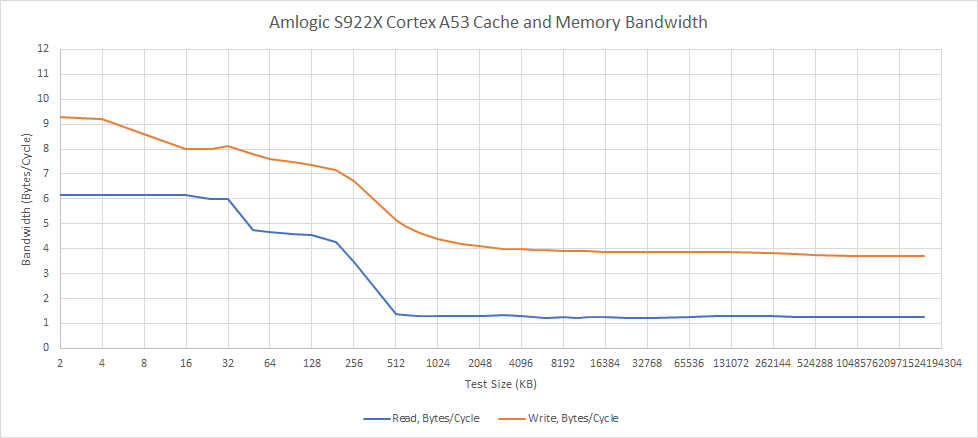
If an access misses the L1D, the cache controller can track up to three pending misses. These misses head on to L2, which is 16-way set associative, and can be configured with 128 KB, 256 KB, 512 KB, 1 MB or 2 MB of capacity. The L2 is a victim cache, which means it’s filled by lines kicked out of L1. As before, ECC protection is optional. An implementer can also entirely omit the L2 cache if they dislike performance. In the Amlogic S922X’s case, the A53 core cluster gets a shared 256 KB cache.

Each A53 core’s L1D has a 128-bit read interface to L2, and a 256-bit write interface. The L2 cache itself has a 512-bit fetch path, which should give it enough bandwidth to service quad core clusters. From measurements, we get just under 8 bytes per cycle in L2-sized regions when writing, and just under 5 bytes per cycle when reading. Even though L2 interfaces should be wide enough to service a memory operation every cycle, we see a drop in bandwidth likely because the L1D can’t track enough in-flight misses to hide latency.
ARM’s technical reference manual suggests the L2 data array can be configured with 2-3 cycles of output latency. L2 load-to-use latency appears to be around 9 ns, or 17 cycles. Latency is therefore quite high, considering the A53 is an in-order core with little ability to hide that latency. I suspect some of this comes from the difficulties of creating a shared cache, which needs to arbitrate between requests from multiple cores.

When servicing both cores, A53’s L2 cache does fairly well. Bandwidth just about doubles when both cores are accessing the cache. With 128-bit vector stores, we can sink about 14 bytes per cycle to a L2 sized region. Again, load bandwidth from L2 is worse, at around 9 bytes per cycle.

The L2 cache complex is also responsible for handling coherency within the cluster. Like Zen’s L3, A53’s L2 maintains shadow tags to track data cached within the cores. These shadow tags are ECC protected, at a granularity of 33 bits. Snoops are only sent to the cores if a request hits those shadow tags, which reduces snoop traffic and makes high core counts feasible. Also like AMD, ARM uses the MOESI coherency protocol. In other words, a cache line can be in one of five states: Modified, Owned, Exclusive, Shared, or Invalid.

Within the A53 cluster, the full speed Snoop Control Unit provides very good performance for cache coherency operations. If a request has to go across clusters, latency is quite high. Moving data between clusters could require a full trip to DRAM. This isn’t unusual, as Qualcomm’s Snapdragon 821 shows similar characteristics. Furthermore, it’s unlikely to have a significant impact on performance, as core to core transfers are far less common than plain cache misses to DRAM.
To handle DRAM accesses, Odroid has equipped the S922X with a 32-bit DDR4-2640 setup. Bandwidth is predictably poor. Writes can achieve 8.32 GB/s, while reads get a bit more than half that amount. In the best case, the A53 cluster on the S922X’s bandwidth will be somewhere close to that of a mediocre dual channel DDR2 setup. The four Cortex A73 cores on the same chip can achieve about 8 GB/s of read bandwidth, so we’re really limited by the memory setup rather than the cores.

DRAM latency is very poor at over 129 ns. High latency and low bandwidth are typical for low power CPUs, but the A53 cluster has things especially hard because it doesn’t have a lot of cache in front of memory. 256 KB is a mediocre capacity for a mid-level cache, and utterly inadequate for a last level one. A lot of memory requests will end up getting served from DRAM, which is horrible for an in-order CPU.
Cortex A53 In Practice
We’re looking at a small, in-order CPU for the first time on Chips and Cheese, so some performance counter data should provide valuable insight. Specifically, we’re getting counter data for these workloads:
Calculate SHA256 Hash: Uses the sha256sum command to calculate the hash of a 2.67 GB file. It’s an extremely simple workload where less than 1% of the instructions are branches. Memory access patterns are very predictable, and cache hitrates are very high.
7z Compression: Uses the 7-Zip program to compress the same 2.67 GB file. This workload challenges the branch predictor a bit, and sees branches often enough that high branch prediction accuracy would help. 7-Zip’s instruction cache footprint is small, but the data-side cache footprint is substantial.
libx264 4K Decode: Decodes a 4K video with ffmpeg. Usually, H264 decoding is not too CPU-heavy. But A53 cores are quite weak and two of them aren’t fast enough to decode H264 in real time at 4K.
libx264 Transcode: Scales down a 4K video to 1280×720 and re-encodes it with libx264, using the slow preset. Video encoding features a large instruction and data footprint, making it quite a difficult workload. Note that this isn’t comparable to previous cases where we tested video encoding, because those used the veryslow preset and encoded at 4K.
From a quick look at IPC, in-order execution can hold its own in specific cases. sha256sum rarely misses cache, so it avoids the achilles heel of in-order execution. Instruction execution latency can still lock up the pipeline, but compilers typically reorder instructions to put independent instructions between dependent ones whenever possible. This static scheduling lets A53 crunch through instructions with few hiccups.

But once you start missing cache, in-order execution quickly falls apart. ARM provides “Attributable Performance Impact” events, which let us drill down on stalls in the Cortex A53’s pipeline. I’ve condensed the events as follows:
Branch Mispredict or Frontend Bandwidth: I’m putting this label on Event 0xE0, which counts “every cycle that the DPU IQ is empty and that is not because of a recent micro-TLB miss, instruction cache miss, or pre-decode error”. DPU IQ refers to the Data Processing Unit’s Instruction Queue. The DPU here is A53’s backend. If its instruction queue is empty, it’s starved of instructions. Excluding TLB and instruction cache misses leaves us with:
Branch mispredicts would flush everything in the IQ fetched after the mispredicted branch
Frontend bandwidth losses around taken branches could under-feed the backend
Instruction Cache Miss: Event 0xE1 is simple, as it counts cycles where the DPQ IQ is empty and an instruction cache miss is pending
Store Bandwidth: Event 0xE8 “counts every cycle there is a stall in the Wr stage because of a store”. Wr appears to stand for “writeback”, and is the final stage in the pipeline where instruction results are committed. Unlike a load, a store doesn’t produce a result that another instruction might depend on. A stall should only be caused if the memory hierarchy blocked the store because too many memory accesses were already pending (i.e., a bandwidth limitation)

Load Missed Cache: Event 0xE7 “counts every cycle there is a stall in the Wr stage because of a load miss”
Execution Latency: Sum of events 0xE4, 0xE5, and 0xE6, which count cycles where there’s an interlock. Interlock means a pipeline delay used to resolve dependencies. These events exclude stall cycles in the Wr stage, so execution latency would be the primary culprit for these stalls.
From these metrics, A53 largely struggles with more complex workloads because of load misses. For example, 7-Zip’s large data footprint makes it incredibly backend-bound. Cache misses create a lot of latency that A53 cannot cope with. We also see cycles lost to execution latency and branching performance. The two are related, because compilers generally can’t reorder instructions across a conditional branch or function call. In 7-Zip, roughly one in every ten executed instructions is a branch. For comparison, sha256sum had a branch roughly once every 100 instructions.
Prediction accuracy is a problem as well, at just 87.76% in 7-Zip. A53’s predictor is getting things right more often than not, but Neoverse N1 achieves over 95% accuracy, and AMD’s Zen 2 gets over 97%. However, losing up to 3.9% of cycles to branch mispredicts is quite acceptable. A53 won’t be running hundreds of instructions ahead of a predicted branch, so mispredicts have relatively low cost. A bigger branch predictor would definitely improve performance, but the scope of possible improvement is small, and probably not worth the power and area cost.

libx264 introduces another layer of difficulty. With a larger code footprint, we start seeing instruction cache miss costs on top of everything else. Branch prediction accuracy is still terrible at under 90%, but libx264 has fewer branches and therefore doesn’t lose as much from branch mispredicts. Execution latency also incurs a high cost, particularly with decoding. AGU interlocks occurred for nearly 6% of cycles, while other integer-side dependencies stalled execution for 4.14% of cycles. SIMD and FP operations in contrast tend to be less latency sensitive. Only 1.36% of cycles in the decode benchmark were spent stalled waiting for a SIMD or FP instruction to produce a result. SIMD and FP execution latency was a bit more of a problem for libx264 encoding, where interlocks related to those instructions accounted for 3.32% of cycles. However, execution latency still caused more stalls on the scalar integer side.
Zooming out, memory access performance is still the elephant in the room. In all three of the non-trivial workloads, A53 spends a massive percentage of cycles with a load miss pending. Improving execution latency or beefing up the frontend would thus only provide limited gains. Because it can’t run far ahead of a cache miss, A53 is at a huge disadvantage compared to out-of-order CPUs.
Of course, memory latency can also be tackled with good caching. Cache hitrates on the S922X look alright, but not great. Because there’s no L3 cache, any L2 cache miss will suffer massively from DRAM latency.

Hitrate is nice for seeing how effective a cache or branch predictor is, but misses per instruction gives a better idea of how performance was affected. We can see that 256 KB of L2 is inadequate for a last level cache. For perspective, the L3 caches on Zen 2 normally see less than 2 MPKI.

Cortex A53’s L1 caches do behave as we would expect for having 32 KB of capacity and a bargain basement replacement policy. 5-10 MPKI would not be out of place on Zen 2, but Zen 2 has a larger and faster L2 cache to catch those misses, and features out of order execution. A53 suffers the worst of all worlds here. It’s in-order, and has an inadequate cache subsystem.
But that’s intentional. A53 is not meant to deliver high performance. Small caches take less area and less power, which are A53’s design goals. Another implementer may opt for larger caches to get more performance out of A53. But that could be an odd choice for a core that doesn’t prioritize performance to begin with.
Final Words
Decades ago, there was quite a debate between in-order and out-of-order execution. Out-of-order execution was very effective in hiding latency and extracting instruction level parallelism. However, it required large, expensive buffers and a lot of hardware complexity. As late as the 2000s, Intel and IBM invested significant effort to produce a viable high performance CPU with in-order processing. These efforts were ultimately unsuccessful; Itanium was discontinued after repeatedly failing to take over the server market. IBM’s in-order POWER6 was succeeded by the out-of-order POWER7, and in-order execution did not return in subsequent POWER generations. In the end, advances in process technology and bigger transistor budgets made the cost of entry to out-of-order execution increasingly irrelevant. The same soon applied to low power CPUs too. Intel’s Tremont, ARM’s Neoverse N1, and AMD’s Jaguar all use out-of-order execution.
But design paradigms that fail in one sector typically don’t fall off the face of the earth. Instead, they find a niche elsewhere, and continue to play a role in our lives even if it’s not flashy enough to dominate headlines. ARM’s Cortex A53 is an excellent example. Avoiding the power and area of out-of-order execution still matters when you’re targeting power levels at 1 watt and below, and trying to save every last bit of core area. The in-order versus out-of-order debate didn’t end. Instead, it was pushed down to lower power and performance points. According to ARM’s keynote presentation, Cortex A53 can deliver the same performance as the 2-wide, out-of-order Cortex A9 while being 40% smaller on the same 32 nm process.
Cortex A53 is able to achieve this because it’s a lot more capable than classic in-order CPUs like Intel’s original Pentium. It has indirect branch prediction, better prediction for direct branches, and dual issue capability for floating point math. Such features make it better suited to the demands of modern workloads, which often see Javascript and other forms of object oriented code.
Of course, there’s room for improvement even if we stay within the constraint of making a 2-wide, in-order core. Bigger and faster caches would help the most. Reducing execution latencies would come next. Then, the core could get a faster and more accurate branch predictor to keep it fed with instructions. But each of those options would incur power and area overhead. And if you’re willing to use power and area to get more performance, the A53 isn’t for you.
In the end, A53 is well balanced at a very low power and performance point. It does reasonably well for a 2-wide, in-order CPU, and ARM has taken care not to chase diminishing returns in pursuit of more performance. The success of this strategy can be seen in how widely A53 was deployed in the mobile market. As further evidence of the design’s strength, it continued to see use in various applications where low power and area are of utmost importance well after its days in cell phone SoCs ended. Those applications don’t need the performance of an out-of-order core, and A53 is right at home there.
If you like our articles and journalism, and you want to support us in our endeavors, then consider heading over to our Patreon or our PayPal if you want to toss a few bucks our way. If you would like to talk with the Chips and Cheese staff and the people behind the scenes, then consider joining our Discord.