
Intel’s Ponte Vecchio: Chiplets Gone Crazy


Intel is a newcomer to the world of discrete graphics cards, and the company’s Xe architecture is driving its effort to establish itself alongside AMD and Nvidia. We’ve seen Xe variants serve in integrated GPUs and midrange discrete cards, but Intel’s not stopping there. Their GPU ambitions extend to the datacenter and supercomputing markets. That’s where Ponte Vecchio (PVC) comes in.
Like other compute-oriented GPUs, PVC goes wide and slow. High memory bandwidth and FP64 throughput differentiate it from client architectures, which emphasize FP32 throughput and use caching to reduce memory bandwidth demands. Compared to Nvidia’s H100 and AMD’s MI210, PVC stands out because it lacks fixed function graphics hardware. H100 and MI210 still have some form of texture units, but PVC doesn’t have any at all. Combine that with its lack of display outputs, and calling PVC a GPU is pretty funny. It’s really a giant, parallel processor that happens to be programmed in the same way you’d program a GPU for compute.

PVC’s physical design makes it even more unique, because it’s a chiplet extravaganza. Compute tiles fabricated on TSMC’s 5 nm process contain PVC’s basic building blocks, called Xe Cores. They sit on top of a 640 mm2 base tile, which contains a giant 144 MB L2 cache and uses Intel’s 7 process. The base tile then acts as an IO die, connecting to HBM2e, PCIe, and peer GPUs. PVC combines five different process nodes in the same package, and connects them using embedded bridges or 3D stacking. Intel has pulled all the stops on advanced packaging, making PVC a fascinating product.
Today, we’re looking at the Intel GPU Max 1100, which implements 56 Xe Cores and clocks up to 1.55 GHz. Its base tile has 108 MB of L2 cache enabled, and connects to 48 GB of HBM2e memory with a theoretical 1.2 TB/s of bandwidth. The Max 1100 comes as a PCIe card with a 300W TDP, making it similar to AMD’s MI210 and Nvidia’s H100 PCIe.
Cache and Memory Latency
Intel uses a two-level caching setup, but with higher capacity and latency than contemporary compute GPUs. To start, each Xe Core gets a massive 512 KB L1 cache. Like Nvidia, Intel allocates both L1 cache and local memory out of the same block of storage. Unlike Nvidia, Intel recognized that our memory latency test doesn’t use any local memory, and gave it the entire 512 KB. L1 latency is reasonably good considering the cache’s size.

If accesses miss the L1, they proceed to access L2 on the base tile. Intel’s L2 cache (sometimes called a L3) is massive, with 144 MB of nominal capacity. We have 108 MB enabled on the SKU we had access to, which is still no joke. A fully enabled AD102 die from Nvidia’s Ada Lovelace architecture has 96 MB of L2 cache, while AMD’s RDNA 2 has up to 128 MB of Infinity Cache. Both architectures represent a recent trend where consumer GPUs are using giant caches to avoid exotic VRAM setups, and PVC’s cache is firmly in the “giant cache” area.

Intel’s L2 latency unfortunately is quite high at over 286 ns. Some consumer GPUs even enjoy lower VRAM latency. I don’t think chiplets are a major culprit, since vertical stacking on AMD’s CPUs only adds a couple extra nanoseconds of latency. Rather, I suspect Intel struggled because they were not used to making big GPUs with big caches. Their Arc A750 has nearly 40% higher L2 latency than the A380 for a 4x L2 capacity increase. Contrast that with a 23% latency increase when going from the RX 7600’s 32 MB Infinity Cache to the RX 6900 XT’s 128 MB one. Larger GPUs with bigger caches tend to see higher latency, but Intel struggles with this more than AMD or Nvidia.

Finally, Intel’s presentation at ISSCC shows the TLB implemented on the base tile, alongside the L2 cache. That suggests the L1 cache is virtually addressed, and hitting the L2 may incur an address translation delay. I’m sure a lot of GPUs do this, but if Intel’s TLB lookups are slow, they would add to cache latency.
High L2 latency may seem pretty bad at first glance, but coping mechanisms exist. PVC’s large 512 KB L1 is as large as L2 capacity on older GPUs, like Nvidia’s GTX 680 or AMD’s Radeon HD 6950. It’s also larger than the L1 mid-level caches on AMD’s RDNA 2 and 3 architectures. Intel’s L1 is really serving as both a first level cache and a mid-level cache. Compared to AMD and Nvidia, Intel’s L2 cache should see far fewer accesses because the L1 will have fewer misses.

We’ve already seen compute architectures experience higher latency than client ones, but PVC takes this another step further. RDNA 2’s Infinity Cache has lower latency than PVC’s L2, despite having similar capacity. VRAM latency is nearly 600 ns, which puts it roughly on par with AMD’s old Terascale 3 architecture. If workloads don’t have good L1 hitrates, Intel’s GPU will need a lot of work in flight to hide latency.
Intel’s A770 is another interesting comparison, because it’s another Xe architecture variant. Like PVC, the A770 has a larger L1 cache than its peers. Its L2 is reasonably sized at 16 MB, putting the A770 somewhere between GPUs with a legacy caching strategy, and newer ones that emphasize massive caching capacity. While A770 appears to take a conservative approach, PVC’s giant L2 cache points towards Intel’s ambitions to combine giant caching capacity with high memory bandwidth to create something special.
Local Memory Latency
Besides global memory, which corresponds to memory as we know it on a CPU, GPUs have local memory that acts as a software managed scratchpad. Intel calls Shared Local Memory (SLM). Nvidia calls the same thing Shared Memory, and AMD calls it the Local Data Share (LDS). Intel’s SLM strategy has varied throughout the years. Their integrated graphics architectures started by allocating SLM out of an iGPU-wide cache. That resulted in poor latency and low bandwidth for what should have been a high performance block of memory, so Intel moved SLM into the subslices (the predecessor to Xe Cores). PVC switches things up again by merging the SLM with the L1 cache.
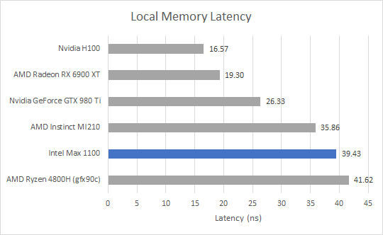
SLM latency is decent on the Intel Max 1100, but isn’t anything to write home about. It’s a bit faster than accessing the same block of storage as L1 cache because there’s no need to check tags and cacheline state.
Compared to other architectures, PVC gets bracketed by GCN and CDNA 2. Consumer architectures from both AMD and Nvidia offer significantly lower latency access to local memory. H100’s shared memory is also very fast.
Atomics Latency
Atomic operations can help pass data between threads and ensure ordering. Here, we’re using OpenCL’s atomic_cmpxchg function to bounce data between two threads. This is the closest we can get to a GPU core to core latency test.
Unlike a CPU, we can test with both local and global memory. We should see the best performance when bouncing data through local memory, because the SLM/LDS/Shmem structure that backs local memory is designed for low latency data sharing. Threads have to be part of the same workgroup to use this method, which means they’re guaranteed to run on the same Intel Xe Core, AMD Compute Unit, or Nvidia Streaming Multiprocessor. It’s a bit like testing core to core latency between sibling threads on a SMT-enabled CPU.

Intel performs reasonably well exchanging data through an Xe Core’s Shared Local Memory. As with the uncontested local memory test, it gets bracketed by two GCN-derived GPUs. Consumer GPUs are again faster. H100 is also quite fast, though not by the same margin as before.
If we use atomic_compxchg on global memory, latency of course is much higher. Intel now falls far behind AMD’s CDNA 2, and very far behind consumer graphics architectures.

In fairness to Intel, bouncing data between threads on a massive GPU isn’t easy. PVC has an incredibly complex interconnect, with cross-die interfaces and a switching fabric on the base die. With that in mind, the Intel Max 1100 only barely loses to Nvidia’s monolithic H100. Intel’s GPU also ties with Nvidia’s Tesla K80, which scored 172.21 ns in this test. Kepler was a very well received architecture and K80 GPUs are so good that they’re still in use today.
Cache Bandwidth
Shared caches need to provide enough bandwidth to service all of their clients. That’s particularly difficult on GPUs, where workloads tend to want a lot of bandwidth. PVC’s L2 cache is special because it’s implemented on a separate base die. All other GPUs (at the time of this writing) place the L2 on the same die as their basic compute building blocks, making PVC unique.

Thankfully, Intel’s 3D stacking interface provides plenty of bandwidth. We peaked at just over 2.7 TB/s with 64 MB of data in play with a different test run that uses 1024 threads per workgroup instead of 256 as on other GPUs. It’s not quite as good as AMD’s MI210 or even H100’s “far” L2 partition. But trading a bit of L2 bandwidth for more capacity seems like a fair choice. PVC does have less memory bandwidth than MI210 or H100, so there’s less bandwidth to service L2 misses with.
We can also see that PVC’s slope is much shallower then the slops for the other GPUs here. Usually, we see bandwidth gently taper off as we get enough work in flight to saturate the cache. Instead, PVC seemingly can’t fully saturate its cache even with over 500 million OpenCL threads being thrown at the GPU to crunch through. For some perspective both MI210 and H100 only needed about 1 million threads to get their high utilization.
PVC may have the biggest L2 cache of any contemporary compute GPU, but it’s not alone in implementing large caches. AMD’s RDNA 2 and RDNA 3 have 128 MB and 96 MB of Infinity Cache, which effectively acts as a fourth-level cache. RDNA 3 implements its Infinity Cache on separate memory controller dies, so its accesses have to go through a cross-die interface just like on PVC. RDNA 2 and Ada Lovelace keep their high capacity caches within a monolithic die.

Intel’s L2 offers similar bandwidth to RDNA3’s Infinity Cache. However, Infinity Cache doesn’t need the same amount of bandwidth as a L2 cache because AMD has a multi-megabyte L2 cache in front of it. Nvidia’s Ada Lovelace needs a lot of L2 bandwidth because it only has 128 KB cache in front of it. Ada’s L1 capacity will be even lower if some of it is used for shared memory. So, Ada’s L2 can deliver nearly 5 TB/s of bandwidth.
VRAM Bandwidth
Consumer GPUs like AMD’s RDNA 2 and Nvidia’s Ada Lovelace have opted for large caches instead of expensive memory configurations, while compute GPUs like MI210 and H100 have done the opposite. Intel’s approach is to do both. A PVC tile features four stacks of HBM2e memory, giving it more memory bandwidth than any consumer GPU. Still, PVC falls a bit short compared to other compute GPUs.

We should see 1228.8 GB/s of theoretical bandwidth, but my test doesn’t get anywhere close. I’m not sure what happened here. Perhaps Intel’s very high memory latency makes it difficult to make use of the bandwidth, and the Xe Cores can’t track enough cache misses in flight to hide that latency.
Compute Throughput
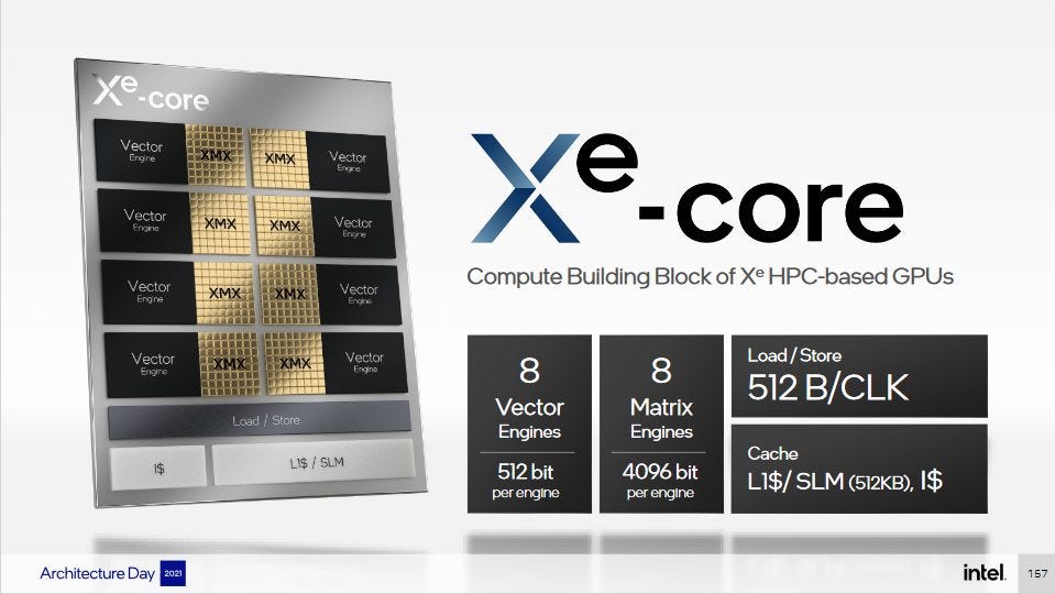
Each Xe Core in PVC consists of eight 512-bit vector engines, which would be good for 16 32-bit operations per cycle. Nvidia and AMD’s designs have settled on using four partitions in their basic building blocks. H100’s SMs have four 32-wide SMSPs, or 1024-bit wide when we consider 32-bit operations. MI210’s CUs have four 16-wide SIMDs, which are also 1024-bits wide because each lane natively handles 64-bit operations.
Intel’s Max 1100 has 56 of these Xe Cores, so it has 7168 lanes running at 1.55 GHz, for a nominal throughput of 11.1 billion operations per second. The MI210’s 6656 lanes at 1.7 GHz should provide 11.3 GOPS, making it similar in size. Nvidia’s H100 PCIe is much larger. With 14592 vector lanes at 1.755 GHz, Nvidia’s monster can do 25.6 GOPS.
Intel makes up some ground if we test instruction rate with 500 million OpenCL threads like we did with cache bandwidth. For reference, FluidX3D’s most common kernel launches with 16 million threads, and a full-screen pixel shader at 4K launches 8 million threads. Our instruction rate test also gets over theoretical throughput, perhaps indicating that the compiler is eliminating some operations. We weren’t able to get to the bottom of this because we don’t have the profiling tools necessary to get disassembly from the GPU.
But even with what looks like an overestimate, AMD’s MI210 has a substantial lead in FP32 throughput if it can use packed operations. Intel can’t do packed FP32 execution but can execute 16-bit integer operations at double rate. FP16 operations can also execute at double rate, though only for adds. This is likely a compiler issue where the v0 += acc * v0 sequence couldn’t be converted into a FMA instruction.

PVC can boost throughput in other ways too. INT32 and FP32 operations can dual issue, giving a substantial performance boost if those operations are evenly mixed. This is true dual issue operation, unlike the claimed “dual issue” on post-Turing Nvidia architectures, where mixing FP32 and INT32 operations won’t get you increased throughput over INT32 alone. Nvidia’s “integer datapath” actually deals with INT32 multiplication. In that respect, PVC and Nvidia follow a similar strategy, and can do 32-bit integer multiplies at half rate. Intel likely carried this strategy over from their integrated graphics architectures. Gen 9 (Skylake integrated graphics) could also do half rate integer multiplication.

Finally, double precision floating point performance is an important differentiator for datacenter GPUs. Consumer grade cards can put up a decent performance in other categories especially considering their price, but generally lack competent FP64 hardware. PVC can do FP64 additions at full rate, but strangely couldn’t do so with FP64 FMAs. I wonder what’s going on here, because their Gen 9 architecture could do FP64 adds and FMAs at the same rate using the same test code.
(Macro) Benchmarks
FluidX3D (FP32)
FluidX3D uses the lattice Boltzmann method to simulate fluid behavior. It uses a variety of techniques to achieve acceptable accuracy without using FP64. Density distribution function (DDF) values are shifted into ranges where FP32 can provide enough precision. DDF summation uses alternating additions and subtractions to reduce loss of significance errors. The result is that FluidX3D can produce results very close to the FP64 “ground truth” while using FP32 operations that perform well on consumer GPUs. I’m using FluidX3D’s built in benchmark here.

Intel’s Max 1100 does not compete favorably against the current crop of compute GPUs from AMD and Nvidia. AMD’s similarly sized MI210 wins by more than 47%, while Nvidia’s giant H100 is three times faster. PVC performs closest to AMD’s RX 7900 XTX, showing that consumer graphics architectures can hit pretty hard in FP32 compute. RDNA 3 combines tremendous FP32 throughput, with caching capacity and memory bandwidth not far off PVC’s, so its performance isn’t a surprise.
Calculate Gravitational Potential
CGP is a workload written by Clamchowder. It does a brute force calculation of gravitational potential, given a map of column density. Code quality is roughly what you’d expect from a typical high school student working on a research project at 3 AM after doing the necessary things to have any chance at college admission (homework for 8 classes, studying for 9 APs, practicing two instruments, playing a sport, and definitely not getting the four hours of sleep recommended in the “sleep four hours pass, sleep five hours fail” saying). In other words, it’s completely unoptimized, and should represent what happens if you’re using hardware time to save human brain time.

Consumer GPUs suffer heavily in this workload because they don’t have a lot of hardware FP64 units, and PVC shows its worth. It’s twice as fast as AMD’s RX 6900 XT, and blows Nvidia’s consumer GA102 chip (A10) out of the water.
However, PVC struggles against recent datacenter GPUs, just as it did in FluidX3D. MI210 outperforms it by a staggering margin by natively handling FP64. H100 does as well, by simply being a massive GPU. PVC also takes a surprising loss to the older Radeon VII, which has a decent 1:4 FP64 ratio.
PVC’s Chiplet Setup
Now that we have an idea of how PVC performs, we can make a few observations on its chiplet setup. PVC’s chiplet setup is fascinating because Intel has chosen to use a more complex chiplet configuration than Zen 4 or RDNA 3. Chiplets are challenging, so that’s risky. Die to die interfaces create area overhead. Data movement between dies is often more expensive than doing so within a monolithic die. Vertically stacked dies can be harder to cool. Successful chiplet implementations mitigate these problems to enjoy cost benefits while suffering minimal performance degradation compared to a monolithic solution.
Lets go over these areas one by one, starting with area.
Area Overhead
Chiplets aim to reduce cost by letting engineers use cheaper process nodes when using better nodes would have limited benefit, and by using smaller individual dies to increase yield. However, chiplets will use more total area than an equivalent monolithic implementation due to duplicated logic and cross-die interfaces. Area overhead can also be more subtle. For example, Zen 4 uses a large and fast L3 cache to mitigate the latency and bandwidth hit of going through an IO die. The fast L3 takes up more die area on a Zen 4 CCD than the cores themselves.

On the area front, Ponte Vecchio uses a 640 mm2 base die. Rough pixel counting gives us the following for the Intel Max 1100:
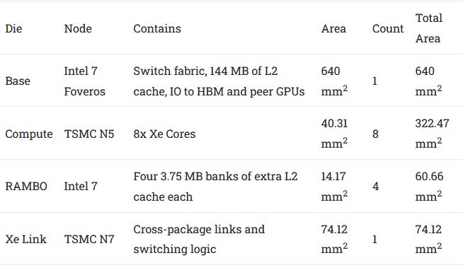
One PVC GPU instance uses 1097 mm2 of total die area across various nodes, excluding HBM. I don’t think any RAMBO cache is enabled on the Max 1100, so we can also consider a 1036 mm2 figure for fairness. AMD’s MI210 uses a 724 mm2 die on TSMC’s N6 process and achieves better performance. Intel is therefore taking at least a 43-51% area overhead. I’m saying at least, because a substantial amount of area is using TSMC’s N5 node, which is more advanced than the N6 node used by AMD. If we use AMD Epyc’s 10% chiplet area overhead as a benchmark, PVC looks unbalanced.
Data Movement
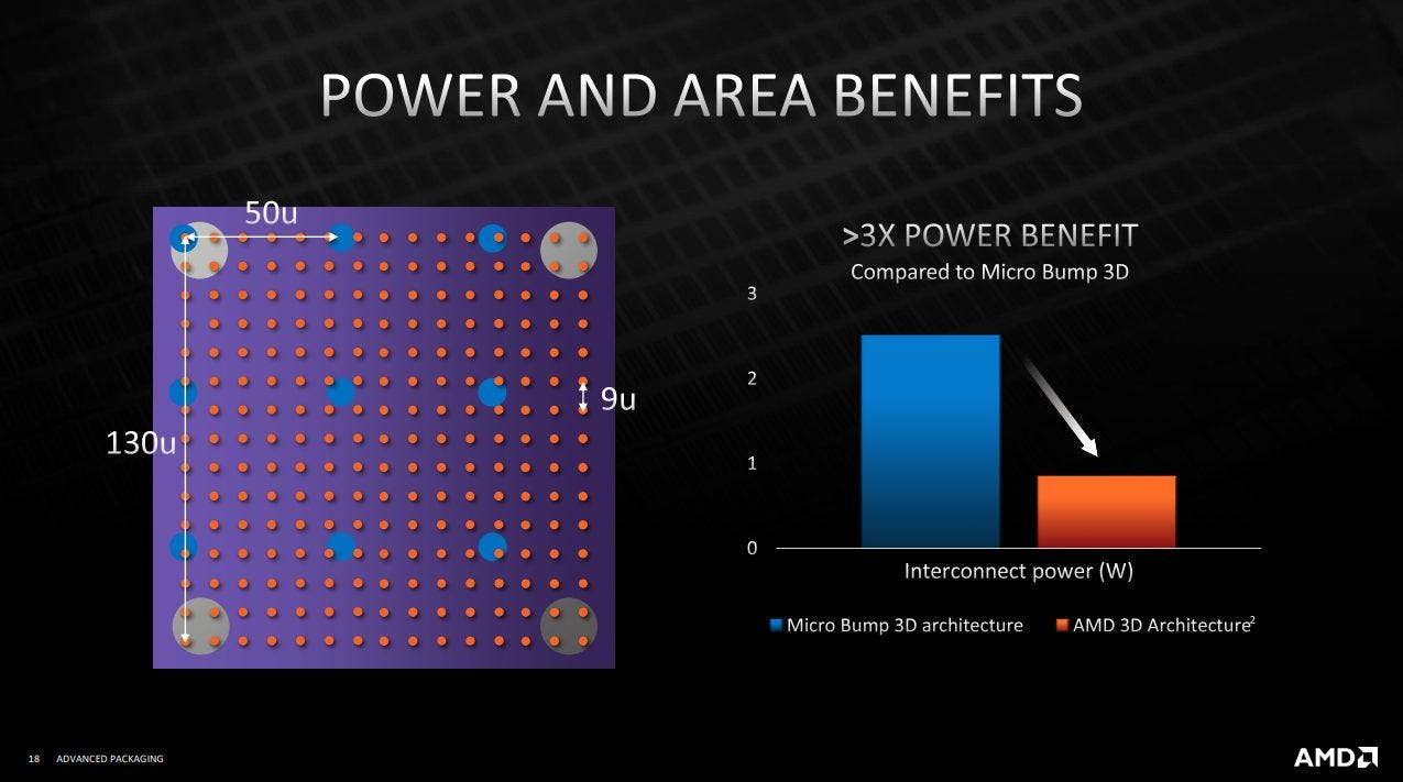
Moving data between chiplets is often more challenging than doing so within a monolithic die. Old Nvidia research estimated 0.54 pj/bit of power draw for cross-chiplet links, but that paper did not consider 3D stacking. AMD showed that 3D stacking could allow massive bandwidth with very little power cost.
On Ponte Vecchio, compute tile to base tile communication would be the highest bandwidth cross-die interface. The L2 cache can provide several terabytes per second, and that’s handled by a 3D stacking interface well suited to such high bandwidth demands. Xe Link and HBM use 2D interfaces, but don’t deal with nearly as much bandwidth. Intel is using the best and highest bandwidth interfaces where they’re needed, making for a sound strategy here.
Cooling
PVC employs 3D stacking in spades. 3D stacking can reduce critical path lengths and package size, but can also create cooling challenges. AMD’s VCache addresses cooling by not stacking any logic over the cores. On my 7950X3D, the VCache CCD clocked 7% lower on average than the non-VCache one. AMD’s MI210 runs at 1.7 GHz, and thus clocks 9.7% faster than Intel’s Max 1100. That’s a problem. PVC puts its shaders on TSMC’s newer 5 nm node, and targets 300W just like MI210. If chiplets are delivering the benefits they’re supposed to, PVC should be pulling ahead.
Intel never published Ponte Vecchio’s die layout, but their slides indicate that IO interfaces are placed around the die edge (as is typical in many designs). IO interfaces shouldn’t get particularly hot, and are covered by “thermal tiles” with no other function other besides conducting heat.

If the compute tiles aren’t overlapping IO, they’re sitting on top of either cache or the switch fabric. Both of those would create heat, which would have to be dissipated through the hot compute tiles. That could exacerbate any hotspot issues within the compute tiles, and force the cooling solution to deal with more heat in the same surface area.
Zen 4 with VCache in comparison only sees a 7% clock speed penalty compared to a vanilla setup without 3D stacking. That’s largely because AMD avoided stacking any cache or logic on top of the CPU cores. In fact, most of VCache’s clock speed deficit appears to come from the vertically stacked cache not being able to handle high voltage, rather than thermal issues. Intel should adopt a similar strategy, and try to overlap compute with cache as little as possible. I don’t think this is an easy change because there’s a massive 144 MB of L2 on the base die, and the switching fabric is likely not small either.
RDNA 3’s chiplet strategy offers an alternative approach. 3D stacking is avoided in favor of putting cache on memory controller dies (MCDs), which use an interposer to get enough cross-die bandwidth. We saw earlier that Intel’s L2 isn’t too much faster than RDNA 3’s Infinity Cache. Certainly RDNA 3’s approach is not without compromises because it’ll make cache bandwidth more difficult to scale. But not all workloads will be bound by last level cache bandwidth, especially with 512 KB L1 caches in play. And higher clock speed could let PVC narrow the performance gap with AMD’s MI210.
Final Words: A Foot in the Door
Compute GPUs like Nvidia’s H100 and AMD’s MI210 push the boundaries of how fast we can process information and are among the most complex chips around. AMD and Nvidia are where they are today thanks to decades of experience building large GPUs. Intel may have a lot of money and good engineers, but they don’t have the same experience. Short of a miracle, their journey to build a big GPU will be an arduous one.
For their part, Intel made it even more arduous by using a chiplet setup with borderline insane complexity. From an outsider’s perspective, they seem to have looked at available nodes and packaging technologies, and decided all of the above would be appropriate. Doing this on any product would be risky, let alone a first entry into a new market.

Intel therefore deserves a lot of credit for not only getting the thing working, but creating a product that’s competent in isolation. Intel’s Max 1100 is a legitimately useful compute GPU capable of decent performance. It’s a far cry from the Moore Threads MTT S80, which uses a conventional monolithic die and fails to match a budget GPU from the Maxwell generation, while failing to run many games.
Of course, Intel has their work cut out for them. Landing between Nvidia’s old P100 and V100 GPUs is not where they want to be. PVC has plenty of weaknesses that Intel has to solve if they want to move up the performance ladder. L2 cache and VRAM latency are way too high. FP64 FMA throughput is curiously low, even in a microbenchmark. For the massive die area investment, PVC doesn’t bring enough compute power to draw even with AMD’s MI210.
With that in mind, Ponte Vecchio is better seen as a learning experience. Intel engineers likely gained a lot of experience with different process nodes and packaging technologies while developing PVC. PVC deployments like TACC’s Stampede3 and ANL’s Aurora supercomputers will give Intel real world performance data for tuning future architectures. Finally, innovations like a giant, expandable L2 cache give the Xe architecture unique flexibility.

Hopefully, we’ll see Intel take lessons and experience from Ponte Vecchio, and develop a stronger datacenter GPU in the coming years.
We would like to thank Intel for allowing us access to a Ponte Vecchio system along with answering some of our questions about Ponte Vecchio.
If you like our articles and journalism, and you want to support us in our endeavors, then consider heading over to our Patreon or our PayPal if you want to toss a few bucks our way. If you would like to talk with the Chips and Cheese staff and the people behind the scenes, then consider joining our Discord.