
NVIDIA’s Next Generation GPU: MCM?

Recently, we’ve heard rumors that NVIDIA Corporation is targeting a MCM design for their next-generation server GPU. While future product details are scarce and volatile, we can guess at Nvidia’s aims by looking at their research. A 2017 paper co-authored by Nvidia lays out the goals and challenges of MCM GPU design.
Sidestepping Moore’s Law Means New Challenges
With SLI’s death, Nvidia was stuck making huge monolithic dies in pursuit of better performance. Monolithic dies are showing their limits. So Nvidia aims to create a scalable, easy-to-manufacture solution with MCM – kind of like AMD’s first generation Epyc/Threadripper offerings. The 2017 paper investigates a 64 SM per-die config and bases it off scaled-up Pascal (Nvidia’s latest arch in 2017)1. With 256 SMs at 1 GHz, this config would achieve 64 TFLOPs.
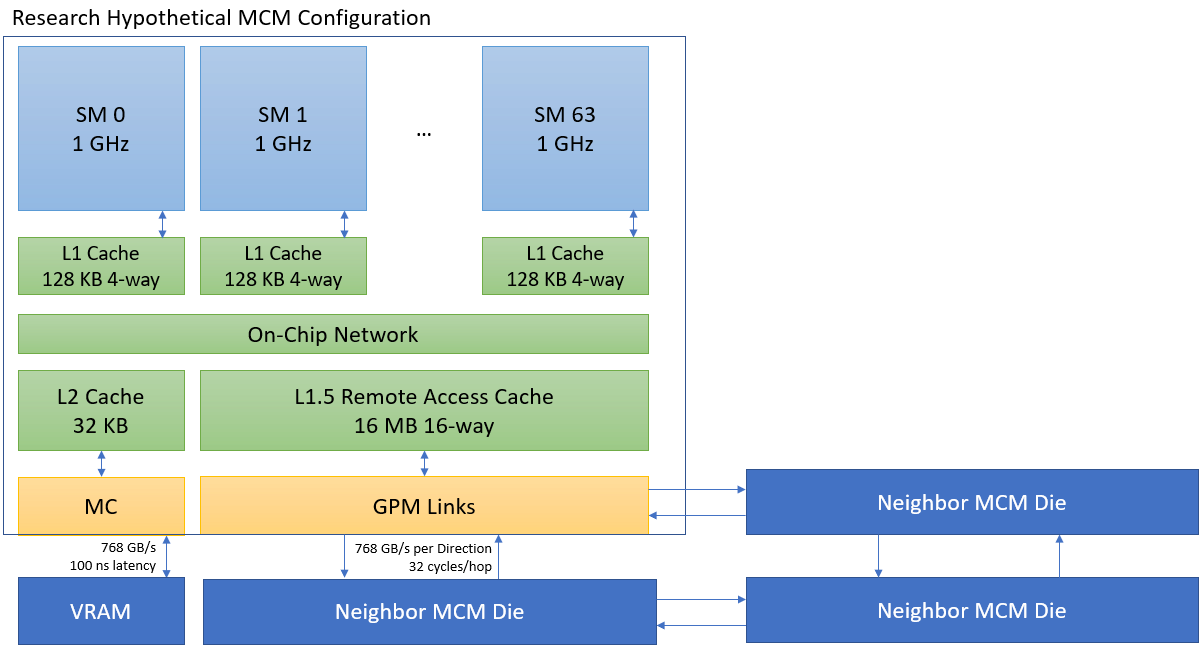

But MCM is not easy. Cross-die data transfers are power hungry and introduce extra latency, compared to transfers within a monolithic die. For die-to-die links, Nvidia’s Ground Referenced Signaling (GRS) on 28nm consumes 0.54 pJ/bit at 20 Gb/s. Nvidia estimates on-die transfers consume 80 fJ/bit1.

Clearly there’s a (power) price to pay with MCM. Make no mistake; a GPU scaled-up via MCM will draw massive amounts of power and require cooling to match. Alternatively, it could be clocked low (like 1 GHz in the paper) and rely on massive parallelism to efficiently deliver more performance. But that hasn’t been the trend recently with consumer parts. The RTX 3080 for example, targets 1710 MHz boost and 320W board power with 68 SMs3. Nvidia will probably want to spend as little power on cross-die transfers as possible, and put that power budget into higher clocks. From the paper, we see a variety of proposed techniques.
Reducing Cross-Die Traffic – All the Tricks…
Caches are the first stop. A 16 MB L1.5 cache is placed in front of the cross-die links, and only reduces cross-die traffic. On average, this L1.5 cache reduced cross-die bandwidth by 28%. Traditional L2 capacity is reduced, down to 32KB. This tiny L2 still sits in front of the memory controller, and helps accelerate atomic operations.
Then, scheduling decisions get tuned to place consecutive thread groups (CTAs) on the same die, hoping to exploit data locality between them. Traditionally, CTAs were round-robin assigned to SMs. The proposed scheme isn’t too different, but tries to fill dies one after another. The 16MB L1.5 synergizes with this when consecutive CTAs wind up sharing data in the L1.5. On average, better scheduling reduced cross-die bandwidth by 33%.
Finally, page mapping decisions are made with the MCM design in mind. When a SM first touches a memory page, it gets mapped to VRAM belonging to its die. This hopefully keeps memory access local to a die. The driver carries out this optimization, opening the door up to further tuning.
Overall, the optimized MCM design reduces cross-die bandwidth by 5x.
How About Graphics and Games – A Thought Experiment
The paper only evaluates compute workloads. So here’s a thought experiment with a graphics workload. On a 4K frame from the FFXIV Shadowbringers benchmark, Nsight Graphics’s speed-of-light metrics indicate 45% VRAM and 33.7% L2 bandwidth utilization on my GTX 1080. GP104’s theoretical L2 bandwidth has been measured to around 980 GB/s4. The GTX 1080’s 256-bit GDDR5X bus provides 320 GB/s of bandwidth. Thus, about 330 GB/s of L2 bandwidth and about 144 GB/s of VRAM bandwidth were used.

That frame took 54.62 ms to render (18.3 fps). If we target 4K 144 fps, or 6.9 ms per frame, we’d consume about 7.9x as much bandwidth. Specifically, 2.6 TB/s of L2 bandwidth and 1.14 TB/s of VRAM bandwidth would be needed. If we simply built a 4-die MCM config, with L2 partitions tied to memory controllers (as it is on current GPUs):

Interestingly, 768 GB/s full duplex links are enough to handle cross-die bandwidth needs in this scenario. An optimized MCM design will of course use less bandwidth. Process enhancements (remember, the paper evaluated 28nm) will also lower link power or increase link bandwidth, while offering further opportunities to reduce cross-die bandwidth needs. Larger caches come to mind.
Because cross-die bandwidth needs can be met with a minor power penalty, manufacturing small dies and scaling out with MCMs can enable massive GPU designs. On the other hand, these MCM GPUs will stretch cooling designs even further, particularly if Nvidia keeps pushing stock clocks to the edge of stability.
Finally, taking advantage of a massive GPU, monolithic or not, presents another challenge. Nvidia readily admits that performance does not scale linearly with compute capacity. 15 of the 48 applications evaluated in the paper don’t spawn enough threads to fully utilize 256 SMs. Developers will need to optimize their workloads to utilize additional parallelism. In conclusion, MCM GPUs are promising. But we may not see the full performance improvements right away.