
Sizing up Qualcomm’s 8cx Gen 3 iGPU

Qualcomm has long harbored ambitions to move up into higher performance segments. Their current Snapdragon 8cx Gen 3 tries to make Qualcomm’s laptop dreams come true, and features in products like Lenovo’s Thinkpad X13s. Laptops have more surface area for cooling and larger batteries, so laptop chips can take advantage of a larger power budget than their cell phone counterparts. GPUs love more power because they handle very parallel tasks, and performance scales well with larger shader arrays. Increased power (and area) budget lets engineers add more execution units.
The Snapdragon 8cx Gen 3 therefore has a large implementation of Qualcomm’s Adreno 6xx architecture. Qualcomm’s GPU naming scheme has the first digit represent the architecture generation, while less significant digits indicate GPU size within a generation. The Adreno 690 on the 8cx Gen 3 therefore is much larger than the Adreno 640 found in cell phone chips like the Snapdragon 855. It also uses an older architecture than Qualcomm’s newest cell phone chips, which have moved to Adreno 7xx.
Thanks to Longhorn, we have Vulkan test data from the Adreno 690. I don’t have the device so I won’t be going too deep into the 6xx GPU architecture, and this will be a short article. Thanks to zarif98 on Reddit, I have been looking at Adreno 640. Its been a slow process because Adreno 6xx has a particularly crashy OpenCL implementation, but hopefully I’ll have stuff figured out soon.
Architecture in Brief
Qualcomm’s Adreno 6xx architecture diverges from Adreno 5xx’s Radeon origins, and adds a separate low priority compute queue to the command processor. This queue lets the driver reserve the primary ring buffer for higher priority tasks, and is meant to allow background compute without display stutters. AMD in contrast jumped in the deep end with multiple asynchronous compute queues.

Adreno also focuses on tile based rendering, which tries to lower bandwidth requirements when rasterizing graphics. Primitives from vertex shaders get sorted into tiles (rectangular portions of the screen), which are rendered one at a time. That improves cache locality, and lets the GPU buffer the render-in-progress tile in specialized memory. Qualcomm calls that GMEM, and Adreno 690 gets 4 MB of that. More GMEM should let Adreno 690 better leverage its larger shader array by handling more pixels at a time. For comparison, Adreno 640 has 2 MB of GMEM.

Mesa source code indicates Adreno 690 has 8 “CCUs”. On Adreno 730, a CCU corresponds to a pair of SPs, or Shader Processors. Adreno 690 likely has a similar design. A die shot of Qualcomm’s 8cx Gen 3 also shows a similar GPU layout with SPs organized in pairs, unlike Snapdragon 821’s Adreno 530.

Therefore, Adreno 690 is a large GPU by Qualcomm standards. It has twice as many SPs as their highest end Snapdragon cell phone chips. Even though it uses a prior generation GPU architecture, its large shader array still demands respect.
Mesa code suggests Adreno 690 has 16 KB instruction caches and 64 KB register files. Each SP’s scheduler probably has two 16 entry partitions, and manages 128-wide waves.
Compute Throughput
Adreno 690’s compute throughput is very close to Nvidia’s GTX 1050 3 GB, and generally competes with the AMD Ryzen Z1’s Radeon 740M iGPU. It’s a tier above the Snapdragon 8+ Gen 1’s Adreno 730.

Like prior Adreno GPUs, Adreno 690 isn’t heavy on special function units and can only execute operations like inverse square roots at 1/8 rate. Nvidia’s Pascal and AMD’s RDNA 2 hit a better 1/4 rate with such operations, though RDNA 3 goes back down to 1/8 rate if we consider FP32 dual issue. Qualcomm heavily emphasizes FP16 throughput, and Adreno 690 excels in that category.
Cache and Memory Latency
Memory performance falls further behind compute every year, so even GPUs have complex cache hierarchies to keep their execution units fed. To match the scaled up shader array, Adreno 690 gets a 512 KB L2 cache. For comparison, the smaller Adreno 640 in the Snapdragon 855 has a 128 KB L2. Then, it shares a 6 MB system level cache with the CPU and other blocks on the chip. Finally, a LPDDR4X memory controller handles DRAM accesses.
Adreno 690’s L2 cache has a hefty 137 ns of latency. L2 accesses on Adreno will have to wait longer for data than on Nvidia’s GTX 1050 3 GB, or AMD’s Radeon 740M. Nvidia and AMD’s GPUs have larger L2 caches as well. Adreno 690 may have a small 1 KB texture cache like Adreno 5xx and 7xx, possibly with 38 ns of latency. But it’s hard to tell because OpenCL can only hit Adreno 690 through OpenCLOn12, which is quite unstable. In any case, Adreno 690 lacks a first level cache with comparable capacity to Pascal or RDNA 3. Nvidia’s Ampere/Ada and Intel’s Xe-LPG/HPG architectures have even larger L1 caches.

After L2, the Snapdragon 8cx Gen 3 has a 6 MB system level cache shared with the CPU and other on-chip blocks. From a latency test, the GPU is able to use about 2 MB of that, much like the Snapdragon 8+ Gen 1’s Adreno 730. System level cache latency is comparable to DRAM latency on older GPUs. Both the GTX 1050 3 GB and AMD’s Radeon 740M can get to DRAM with less latency. If Adreno 690 has to pull data from DRAM, latency is high at over 400 ns.
Bandwidth
The highly parallel nature of GPUs makes them high bandwidth consumers. GPU caches have to satisfy those bandwidth demands in addition to reducing stalls due to memory latency. While Adreno 690 had comparable compute throughput to AMD’s Radeon 740M and Nvidia’s GTX 1050 3 GB, it has far less bandwidth available to feed those execution units.
AMD’s RDNA architecture traditionally has very high first level bandwidth. The company’s prior GCN architecture already had decent 64 byte per cycle L1 caches, but RDNA doubles that to 128 bytes per cycle to match its 32x 32-bit wide vector execution scheme. Pascal has 64 byte per cycle L1 texture caches, though the Vulkan test here can’t see the full bandwidth. Texture accesses via OpenCL can achieve 1274 GB/s from the GTX 1050 3 GB. Qualcomm is very far behind, and that disadvantage extends to L2.

Adreno 690 only has a bandwidth lead when it can leverage the system level cache. There, Adreno 690 can sustain 130 GB/s, while the GTX 1050 3 GB and Radeon 740M are limited by DRAM. At larger test sizes, Nvidia’s GTX 1050 3 GB technically wins thanks to its high speed GDDR5 memory. LPDDR-6400 lets the Radeon 740M come in just a hair behind. Finally, Adreno 690’s older LPDDR4X trails at just under 60 GB/s.
Link Bandwidth
iGPUs can enjoy faster data movement between CPU and GPU memory spaces because they’re backed by the same memory controller. That holds true for Adreno 690 too. Copies between CPU and GPU memory spaces can exceed 26 GB/s of bandwidth. For comparison, Nvidia’s GTX 1050 3 GB is limited by its PCIe 3.0 x16 interface.
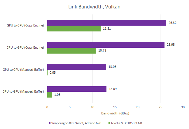
Adreno 690’s advantage continues if the CPU uses memcpy to get data to and from GPU memory. For an iGPU, it’s basically a CPU memory bandwidth test. When the Core i5-6600K tries to do the same to data hosted on the GTX 1050 3 GB’s GDDR5, bandwidth is extremely low because the CPU cores can’t cope with PCIe latency.
Final Words
Qualcomm’s Adreno 690 is an interesting look at a mobile-first company’s attempts to move into higher power and performance segments. Adreno 6xx’s shader array gets scaled up, bringing its compute throughput close to that of Nvidia’s GTX 1050 3 GB and AMD Ryzen Z1’s integrated Radeon 740M. Its L2 cache gets a corresponding capacity boost to 512 KB. But Qualcomm’s iGPU still lacks cache bandwidth compared to those AMD and Nvidia designs. Adreno 690 further suffers from higher latency throughout its memory hierarchy, so it’ll need a combination of higher occupancy and more instruction level parallelism to hide that latency.
However, the Snapdragon 8cx Gen 3’s 6 MB system level cache can help take the edge off memory bandwidth bottlenecks. Furthermore, Qualcomm has long relied on tile based rendering to handle rasterization with lower memory requirements. That could let Adreno 690’s sizeable shader array shine, as GMEM helps absorb writes to a tile until the finished result gets written out to main memory. However, newer games are increasingly using compute shaders and even raytracing. Tile based rendering’s benefits could be limited if the traditional rasterization pipeline starts taking a back seat.
Today, the Snapdragon 8cx Gen 3 is a couple years old. Qualcomm is looking to continue their laptop push with a new generation of chips that can reach 80 watt “device TDP” figures. That applies to an entire laptop, but CPU/GPU power consumption under load likely accounts for most of that 80W. My Meteor Lake laptop idles at 3-4 watts for example. Using that as an estimate for platform power would leave a good 75W left for the SoC under load, with a fan potentially consuming a couple extra watts.
With such a power target, Qualcomm will be hitting territory traditionally occupied by laptops with discrete GPUs. I look forward to seeing how those future devices stack up.
If you like our articles and journalism, and you want to support us in our endeavors, then consider heading over to our Patreon or our PayPal if you want to toss a few bucks our way. If you would like to talk with the Chips and Cheese staff and the people behind the scenes, then consider joining our Discord.