
Inside Snapdragon 8+ Gen 1’s iGPU: Adreno Gets Big

Mobile SoCs have come a long way over the past eight years. I previously covered the Adreno 530 in Qualcomm’s Snapdragon 821, which had to do its best within a tiny power and thermal envelope using a now outdated 14 nm process. Now I’m using an Asus Zenfone 9 with a much newer Snapdragon 8+ Gen 1. It’ll be very interesting to see what Qualcomm did with the GPU given more than seven years of engineering time and TSMC’s much better 4 nm process.

Designating the architecture is funny. Qualcomm used to have a gxx GPU naming scheme. ‘g’ would denote the architecture generation, while larger ‘xx’ values would indicate larger GPU implementations. Under the brilliant and fearless leadership of their ever-victorious marketing department, Qualcomm has abandoned this naming scheme and replaced it with absolutely nothing. All Qualcomm GPUs in their latest products are simply called Adreno.
Thankfully, the prior naming scheme still exists internally. The Snapdragon 8+ Gen 1’s iGPU identifies as an Adreno 730 to the CPU-Z app, and uses that designation within driver code. The 7xx prefix indicates Adreno 730 uses a newer architecture than the Adreno 6xx iGPU used in the Snapdragon 888. With a -30 suffix, the Adreno 730 is a smaller implementation of the 7xx architecture than the Adreno 750 in Qualcomm’s newer Snapdragon 8 Gen 3. But you wouldn’t know that from Qualcomm’s marketing materials.
High Level
Adreno 730 is faster and bigger than its 530 series counterpart from two architectural generations ago. Snapdragon Profiler reports a 900 MHz maximum clock speed. That’s higher than Adreno 530’s 653 MHz, but still far off what we see from discrete GPUs even a decade ago. Instead of clock speeds, Adreno 730 gets most of its throughput increase from a wider shader array. It comes with twice as many cores, which Qualcomm calls Shader Processors (SPs). Each SP has doubled compute resources compared to the ones on Adreno 530, further increasing throughput. Adreno 730 reports 4 “Compute Units” through OpenCL, but based on compute throughput available to each workgroup and the number of texture cache instances, I believe there are eight SPs.
All of the SPs share a L2 cache, which sees capacity doubled to 256 KB. Beyond L2, Adreno 730 benefits from a more modern SoC design and shares a 4 MB System Level Cache (SLC) with the CPU. That gives it a triple level cache hierarchy.

For VRAM, Adreno 730 shares the Zenfone 9’s 8 GB of LPDDR5 with the CPU. This memory runs at 3200 MHz, and provides 51.2 GB/s of theoretical bandwidth. Adreno 530 in the LG G6 has 4 GB of LPDDR4 running at 1866 MHz with a dual channel setup. If each channel is 16 bits wide, that would provide 14.9 GB/s of bandwidth. Therefore, new memory technology gives Adreno 730 several times as much memory bandwidth, which should go a long way to keeping the bigger GPU fed.
OpenCL reports that Adreno 730 can use 3.54 GB of system memory, while Adreno 530 is limited to 1.85 GB. A single allocation can use up to 906 MB on Adreno 730, up from 472 MB on Adreno 530.
Adreno 730’s Shader Processor
Shader Processors (SPs) are the basic building blocks in Qualcomm’s Adreno GPUs, and are roughly comparable to Nvidia’s SMs or AMD’s RDNA WGPs. Adreno 730’s SPs feature twice as many execution units as Adreno 530’s and use a wider vector width, but are otherwise similar.

A SP first fetches instructions from a 16 KB instruction cache, which can be pre-loaded by the driver to reduce warm-up time. Instructions are then decoded and their inputs read from the vector register file. Mesa code suggests Adreno 730 has 64 KB of vector registers per SP partition.
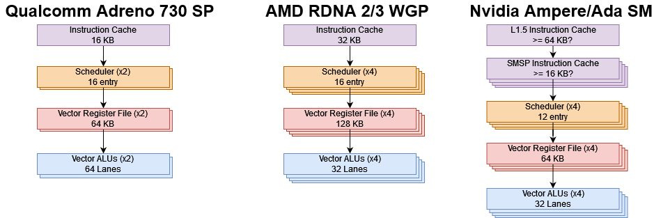
GPUs hide memory and execution latency using wide vectors and thread level parallelism. To that end, Adreno 730’s SP can keep 32 threads in flight across its two scheduler partitions. Each thread’s instructions operate on 2048-bit vectors (wave64), so Adreno 730 has twice the vector width of Adreno 530. Vector width thus continues to match execution unit width. Effective thread level parallelism can often be limited by register file capacity. Wave64 mode and a 64 KB register file mean Adreno 730 will probably behave like AMD’s GCN, but can keep more work in flight if a kernel uses 16 or fewer registers.
Wave64 mode lets Adreno 730 do twice as much work per instruction fetch as Adreno 530. However, that also makes Adreno 730 more susceptible to divergence penalties. If I run a compute throughput benchmark where threads do either FP32 additions or multiplications depending on the outcome of a conditional branch, Adreno 730 sees reduced throughput when threads within a 64-wide block take different branch directions.

That’s because GPUs handle divergent branches by executing both sides of a branch, with lanes that didn’t take the branch masked off. Nvidia’s Pascal architecture in the GTX 1050 3 GB is less prone to losing throughput like this thanks to its narrower 32-wide vector width.
Compute Throughput
Once the scheduler selects a thread to execute and its operands are read from the register file, the execution units can start working on it. Alongside the switch to wave64, Adreno 730 doubles execution resources in each scheduler partition. The SP’s throughput thus matches Nvidia’s SM or AMD’s RDNA WGP, at least for the most common and basic operations. It also matches Nvidia and AMD’s current designs in aligning execution unit width to wave width.

More SPs, bigger SPs, and higher clocks give Adreno 730 a giant increase in floating point throughput compared to Adreno 530. As mobile GPUs benefit from newer process nodes that offer impressive improvements for low power devices, I thought it’d be interesting to compare with Nvidia’s GTX 1050 3 GB. The GTX 1050 3 GB represents a budget discrete card from a few generations ago. It can still competently run games like Valheim at 1080P, though with some settings turned down. A GPU of its caliber can still squeeze by at low settings when presented with all but the most demanding PC titles.

In basic operations, Adreno 730 feels like it’s a tier under Nvidia’s old Pascal cards. It could close the gap if games use enough FP16 operations, since Adreno can execute those at double rate. That’s highly workload dependent of course. Through Qualcomm’s Snapdragon Profiler too, I observed Fallout Shelter executing slightly fewer half precision (16-bit) instructions than full precision (32-bit) ones in fragment shaders. 3DMark’s Sling Shot Extreme benchmark in contrast almost exclusively uses full precision.

Special operations like reciprocals and inverse square roots execute at 1/8 rate, so Adreno 730 is light on special function hardware compared to Pascal or AMD’s RDNA. Those architectures feature 1/4 rate execution for special functions. However, Nvidia has taken a similar approach with their newest architectures, which also execute such operations at 1/8 rate.
Integer throughput tells a similar story, with Adreno 730 landing about a tier below Nvidia’s old discrete card. INT64 throughput remains atypically weak. Adreno 530 has a problem with 8-bit integer operations, which Adreno 730 fixes.

Overall, Adreno 730’s SP looks a lot like an Adreno 530 one but with everything doubled up and some problems fixed. With eight SPs, Adreno 730 is wide enough to draw comparisons with budget desktop GPUs from half a decade ago. But working within a passively cooled cell phone is hard even with several generations of process node and architecture advancements, and Adreno 730’s still very low clock speed prevents it from directly competing with the GTX 1050 3 GB.
Cache and Memory Access
Wide vector processors like GPUs can demand a lot of memory bandwidth, so GPU cores often have very high bandwidth memories attached to them.

Local Memory
Unlike CPUs, GPUs offer small directly addressed on-chip memories. OpenCL exposes this through the Local Memory space. Software has to explicitly move data into Local Memory. But once it does, data stored in Local Memory can be accessed with low latency and high bandwidth. Local Memory is also “local” because its contents are local to a workgroup of threads.
Adreno 730 no longer has the “one workgroup per SP” limitation that plagued 5xx Adrenos, but that also makes determining usable Local Memory capacity more difficult than just looking at the maximum allocation reported through OpenCL. I therefore measured Local Memory capacity by adapting my GPU memory latency test. I made it allocate Local Memory, then checked how many copies of the test I can spawn in different workgroups before the the GPU couldn’t keep them all in flight. I determined that Adreno 730 has 256 KB of local memory available, matching the 32 KB per SP that Adreno 530 had.

Nvidia Pascal’s SMs have 96 KB of Local Memory, though I was only able to see 88 KB when each workgroup allocates 4 KB (or 90 KB with 6 KB per workgroup). Despite having more Local Memory capacity, the GTX 1050 3 GB still enjoys better latency. Adreno 730 does improve over the Adreno 530, but low clock speed still holds it back. Current AMD and Nvidia architectures enjoy even faster Local Memory access than Pascal.

Local Memory is also a good way for threads in the same workgroup to exchange data and synchronize. Bouncing data between threads using OpenCL’s atomic_cmpxchg function actually shows a small regression going from Adreno 530 to 730.

Again Pascal wipes the floor with very low latency data exchange between threads. Atomic operations seem rare for graphics code, so regressing here may be excusable.
Adreno 730 offers a massive increase in Local Memory bandwidth compared to Adreno 530. I got the highest bandwidth results with float4 accesses, which provide more instruction level parallelism than scalar accesses. That’s about 59.68 bytes per SP cycle, so the SP likely has a 64 byte per cycle bus to Local Memory. In any case, Adreno 730’s SPs have twice as much per-cycle Local Memory bandwidth as Adreno 530’s.

Pascal’s SMs can load 128 bytes per cycle from Local Memory, giving it a huge bandwidth advantage. Adreno 730’s 430 GB/s is nothing to sneeze at especially on a mobile chip, but it’s nowhere near the GTX 1050’s nearly 1.3 TB/s.
L1 Texture Cache
Local Memory is fast, but its low capacity and software managed nature makes it difficult to leverage. With caches, hardware automatically manages what’s stored in the cache, letting software transparently get a speed boost.
Like Adreno 530, Adreno 730’s cache hierarchy starts with a tiny 1 KB texture cache. It’s a read-only cache with no coherency support, so it’s only enabled for texture accesses. Pascal’s texture cache faces similar limitations, but has 24 KB of capacity. As with Local Memory, Adreno 730’s SPs enjoy twice as much per-cycle bandwidth from their texture cache compared to Adreno 530. Pascal’s texture cache also delivers 64 bytes per cycle, but each Pascal SM has two of them. Again, that gives Pascal a giant cache bandwidth advantage.

To Qualcomm’s credit, Adreno 730 offers a lot more L1 bandwidth than Adreno 530. But Adreno still does not have the L1 bandwidth to compute ratio that discrete GPUs enjoy.

Adreno 730’s L1 latency improves to 62.33 ns, but Pascal is again a step ahead. Newer AMD and Nvidia GPUs offer even better L1 latency.
L2 Cache
Adreno 730 has a 256 KB L2 cache that’s shared across all SPs, which services L1 texture cache misses and acts as the first level cache for compute memory accesses. It’s a read-write cache, making it more suitable for compute code.
Latency is slightly higher than in Adreno 530’s 128 KB L2, but Qualcomm still offers lower latency access than Pascal does. The GTX 1050 3 GB however does have three times as much L2 capacity.

Pascal also has more L2 bandwidth, though in fairness Pascal has exceptional L2 bandwidth for a GPU of its time.

Again, Qualcomm’s 4 nm chip blows their older 14 nm one out of the water.
Because the L2 cache is shared across all of a GPU’s cores, it’s also a good place to implement global memory atomics. We can test this with a GPU core to core latency test of sorts, using OpenCL’s atomic_cmpxchg function. Adreno 730 regresses compared to its equivalent from two generations ago, possibly because the intra-GPU interconnect struggles with the larger design.

The GTX 1050 3 GB can bounce values between threads across the GPU with half as much latency. Nvidia has a lot of experience building interconnects for gigantic desktop and datacenter GPUs. Tying 6 SMs together on the GTX 1050 must have been a cakewalk.
System Level Cache
DRAM accesses can be both power hungry and low performance. Mobile SoCs have a lot of blocks that need to access DRAM, but implementing a large cache for each would be a waste. Therefore, recent mobile SoCs use a System Level Cache (SLC) that’s shared by various blocks including the CPU and GPU. The Snapdragon 8+ Gen 1 has a 4 MB SLC.
Because it’s logically closer to the memory controllers than any blocks on the chips, latency isn’t great. With just above 243 ns of load to use latency, getting data from the SLC takes longer than doing so from the GTX 1050 3 GB’s GDDR5 VRAM.

Even though the Snapdragon 8+ Gen 1 has a 4 MB SLC, it looks like the GPU can only use 2 MB of it. I see a clear latency jump past 2 MB. I can’t get a full-GPU bandwidth test to clearly show jumps at cache levels (as Nemes is able to with her Vulkan suite), but I can do that if I use a single workgroup. That’s because I won’t have issues where shared cache or memory controllers combine requests from different SPs.

As with latency, there’s a clear drop in performance after 2 MB. Qualcomm may be statically partitioning SLC capacity to prevent the CPU and GPU from continually kicking out each other’s data. Even 2 MB of last level cache is quite decent though, and makes Adreno 730’s shared cache setup look a bit like that of integrated RDNA 3 GPUs. For example, the Radeon 780M in AMD’s Phoenix APU has a 256 KB L1 mid-level cache for each set of three WGPs, and a 2 MB L2 that acts as a GPU-wide last level cache.
I measured about 73.56 GB/s of bandwidth from the SLC with a 1.5 MB test size. That’s almost as much bandwidth as Adreno 530 can get from its L1 cache.
DRAM Access
The Snapdragon 8+ Gen 1 features a 64-bit LPDDR5 interface, which probably runs at 3200 MHz to provide 51.2 GB/s of theoretical bandwidth. I measured just under 50 GB/s. It’s a massive improvement over the Adreno 530’s LPDDR4 setup.

Discrete cards like the GTX 1050 however still enjoy a large advantage. Their DRAM configurations can be specialized to provide high bandwidth, while iGPU memory setups are often a compromise. My test overestimates bandwidth on the GTX 1050 3 GB, which should be just 84 GB/s.
Memory latency is slightly high on the Adreno 730 when compared to modern GPUs. It regresses compared to the Adreno 530, and having to check the SLC on the way to memory could contribute to this higher latency. Both Adreno GPUs see latency skyrocket as the test array gets very large, possibly due to TLB misses. If so, Adreno 730 improves TLB coverage to 48-64 MB, compared to 16 MB on the Adreno 530.

Nvidia’s Pascal architecture generally enjoys excellent VRAM latency, and the GTX 1050 3 GB is no exception.
CPU to GPU Copy Bandwidth
Integrated GPUs can enjoy an advantage over their discrete counterparts when moving data between CPU and GPU memory spaces. Discrete cards are limited by their PCIe interface, which is often slower than a CPU’s DRAM bus.
For small copy sizes, Adreno 730 enjoys massive CPU to GPU copy bandwidth likely because transfers are contained within the Snapdragon 8+ Gen 1’s System Level Cache. Performance with larger copy sizes is less impressive, but still good compared to the 16 GB/s of theoretical bandwidth available with a PCIe 3.0 x16 interface. The older Snapdragon 821 lacks a System Level Cache, but still gets reasonable copy performance.

Nvidia’s GTX 1050 3 GB has a harder time, falling well short of what the PCIe 3.0 x16 interface should provide. But things turn around when getting data from VRAM back to the CPU side. Both Adreno GPUs are terrible at it. Adreno 730 averages just 1.6 GB/s across all test sizes with little variation. It’s several times better than Adreno 530’s 370 MB/s average, but Nvidia’s GTX 1050 3 GB shows what performance should be like with an average bandwidth of just over 6 GB/s.

Qualcomm may have optimized the GPU’s copy engine exclusively for moving data from CPU to GPU memory space. That make sense because games have to copy a lot of textures and other data into GPU memory to get rendering done, but don’t care about getting the results (rendered frames) back. Frames are displayed on the screen and then simply overwritten by the next one.
In contrast, GPGPU compute applications may split processing between the CPU and GPU, and therefore need to read results back from the GPU. Nvidia (and AMD) have optimized their copy engines to move data in both directions.
Graphics Performance: 3DMark
3DMark’s Wild Life Extreme test uses the Vulkan API, and can run in an offscreen unlimited mode for chip-to-chip comparisons. Unlimited mode renders at a fixed 3840×2160 resolution and aims to output identical frames regardless of what device it’s run on.

Nvidia’s low end card is about 50% faster than Adreno 730, and has roughly the same compute throughput advantage at its 1.8 GHz boost clock. Compared to the admittedly low end iGPU included with AMD’s Zen 4 desktop parts, Adreno 730 offers three times the performance. Again, performance isn’t far off what you’d expect looking at the size of the GPU’s shader array. That’s a good performance from Qualcomm. They’re able to feed the shader array about as well as AMD and Nvidia can, even though a glance at average FPS indicates none of these GPUs are well suited to 4K gaming.

3DMark Wild Life largely leverages the traditional rasterization pipeline with a modest amount of compute mixed in.
Compute Performance: FluidX3D
FluidX3D uses the Lattice Boltzmann method (LBM) to simulate fluid behavior. Because LBM can be memory bandwidth constrained, FluidX3D can be compiled to use FP16 storage. Its FP16S mode uses the IEEE-754 standard 16-bit floating point format, while FP16C uses a custom FP16 format with a 4-bit exponent and 11-bit mantissa. FP16 values are still converted to FP32 for computation, so using those modes serves to trade memory bandwidth and storage requirements for increased compute requirements.
For Adreno, I’m running a reduced version of the benchmark. FluidX3D by default benchmarks with a 256x256x256 grid. However, that grid size would require 1.2 GB from a single allocation. Adreno 730 can’t handle an allocation larger than 906 MB. So, I’m using a 128x128x128 grid.

Despite two generations of improvements, Qualcomm continues to get pummeled in this workload. Adreno 730 gets some credit for delivering a 2-4x performance improvement depending on mode, but Qualcomm’s iGPUs are still off by a few orders of magnitude.
Results like these are why I think Intel deserves a lot of credit for getting Ponte Vecchio working as well as they did. AMD’s MI210 is 47% faster than Intel’s Data Center Max 1100. That difference is certainly noticeable, but running FluidX3D on Intel’s card is still practical. Nvidia’s GTX 1050 3 GB is ~292 times faster than Adreno 730. FluidX3D is basically unusable on Qualcomm’s GPU. Getting an architecture to work reasonably well across a wide range of applications is difficult, and the results here demonstrate that.
Rasterization Optimizations
So far I’ve focused on evaluating Adreno 730 from a compute perspective. That’s because I’m not familiar enough with graphics programming to write microbenchmarks using APIs like DirectX or OpenGL. But leaving graphics out wouldn’t be fair because Qualcomm appears to have focused heavily on the rasterization pipeline, and A7xx architecture changes continue that focus.
Therefore, I’ll look at Freedreno and Linux kernel code that shows Adreno’s optimizations for graphics rendering.
Command Processor Changes
GPU drivers launch work on the device by writing command packets into a special ring buffer. Adreno’s Command Processor (CP) parses these packets and distributes work across the shader array. Adreno 5xx’s CP was split into a Prefetch Parser (PFP) and Micro Engine (ME) in a manner similar to AMD’s Radeon GPUs. Adreno 6xx unified the two into a SQE processor, and adds a LPAC processor for low priority asynchronous compute.

A7xx takes A6xx’s SQE and splits it into separate BR (binning rendering?) and BV (binning visual?) processors. Like the prior PFP+ME scheme, BR and BV don’t run in sync and could require synchronization. Unlike ME+PFP where PFP processes certain packets ahead of ME to speed up command processing, BR+BV is meant to carry out what Qualcomm calls “concurrent binning”. Adreno uses tile based rendering to maximize efficiency which involves dividing a frame’s pixels into bins (binning) to hopefully fit data needed to rasterize them into cache.
Concurrent binning allows the binning pass to proceed in parallel with the rendering pass for a prior frame. Thus A7xx’s BR+BV setup also helps accelerate command processing, but with a specific focus on rasterization. The BR+BV strategy contrasts with how AMD has created separate ACE (Asynchronous Compute Engines), which expose separate compute command queues alongside the primary graphics focused one.
More GMEM
Adreno has an internal GMEM buffer that assists in tile based rendering by acting as a local color and depth buffer for the tile being rendered. Ideally, Adreno only has to copy out the final pixel colors in a tile to system memory, with GMEM handing intermediate outputs.

Adreno 730 has 2 MB of GMEM capacity, which is twice as big as Adreno 530’s 1 MB. In conjunction with its larger L2 cache, Adreno 730’s big GMEM buffer may let it use bigger tiles that better fit its wide shader array. As to Qualcomm’s goals, giving GMEM 2 MB of capacity while keeping caches small shows a sharp focus on rasterization. I don’t know of a way to use GMEM from compute kernels.

In contrast, render backends in AMD and Nvidia architectures exclusively leverage the GPU’s general purpose cache hierarchy. AMD’s RDNA architecture makes the render backend a client of the L1 cache, while Nvidia’s Pascal architecture has it work with L2.

Pascal and RDNA both have multi-megabyte L2 caches that offer as much (or more) caching capacity than Adreno 730’s GMEM. A larger L2 can benefit non-graphics workloads as well.
Visibility Stream Compressor
Once an Adreno GPU figures out where geometry is, it creates “Visibility Streams” that appear to contain triangles that overlap a tile. They’re then written to system memory through the L2 cache. This contrasts with the immediate mode rasterizer in Terascale, which reserves storage for primitive coordinates in a 3.8 KB position buffer. Using system memory to pass data between graphics pipeline stages allows tiled rendering to proceed regardless of how many primitives overlap a triangle, but increases demands on a scarce and power hungry resource on a mobile SoC.
The Visibility Stream Compressor (VSC) compresses those Visiblity Streams to reduce bandwidth demands.

Adreno 730 has a scaled up VSC with 32 pipes, twice that of the 16 pipes in Adreno 530’s VSC. That should improve geometry throughput.
Final Words
Qualcomm iGPUs have come a long way since Windows 10 was demo-ed on a Snapdragon 820, equipped with the Adreno 530. Adreno 730 benefits from two generations of architectural development (or at least that’s implied by its unofficial name), a much better process node, and a new generation of DRAM technology. With that improved foundation, Adreno 730 has several times more compute performance and bandwidth. In fact, Adreno 730 can provide Steam Deck like FP32 throughput. That’s impressive for a cell phone SoC, which has to operate without active cooling.
Beyond scaling up the shader array, fixed function hardware sees big changes. The command processor has been overhauled to optimize tiled rendering. More GMEM saves bandwidth when rendering tiles, and more VSC pipes help accelerate compression of primitive data streams. Those changes should make Adreno 730 a force to be reckoned with for rasterized graphics.
But I’m surprised at how little Qualcomm has changed their Shader Processor over seven years and two major architecture generations. Adreno 730’s SPs continue to have a tiny 1 KB texture cache and 32 KB of local memory, just like Adreno 530’s SPs. The L1 bandwidth to compute ratio remains unchanged, as does the L2 capacity to SP ratio. Adreno 730 does double SP execution lane count and vector width, but Qualcomm adjusts those parameters to create different GPU SKUs within a generation. From the compute perspective, Adreno 730 feels like a bigger Adreno 530 with bugfixes.

Qualcomm’s approach contrasts with AMD and Nvidia’s, which treat both compute and graphics as first class citizens. Both high end GPU manufacturers made notable improvements to their GPU “cores” over the past seven years. Nvidia’s Turing replaced Pascal’s read-only texture cache with a read-write L1 cache, letting both texture and generic compute accesses benefit from L1 caching. AMD and Nvidia’s recent GPUs also feature higher cache bandwidth. And while Adreno benefits from a System Level Cache, AMD and Nvidia both give their discrete GPUs absolutely gigantic last level caches.

Nvidia and AMD’s architectures are thus well positioned to handle games that more heavily leverage compute. Compute calls don’t expose the primitive info necessary to carry out tile based rendering, which could cut into the benefits Qualcomm sees from focusing on tiled rendering.
I’ll be interested in seeing how Qualcomm adjusts their GPU architecture in the future. Their upcoming Snapdragon X Elite looks to target 80W device power levels, suggesting it can take on demanding PC titles at reduced settings. As we know from Intel’s efforts, reaching for higher GPU performance and power targets can be quite arduous.
If you like our articles and journalism, and you want to support us in our endeavors, then consider heading over to our Patreon or our PayPal if you want to toss a few bucks our way. If you would like to talk with the Chips and Cheese staff and the people behind the scenes, then consider joining our Discord.
If you can, you should redo this with the new 8 Elite. It has a giant 12MB of GMEM and quite a few architectural changes too in hardware.
Would love to get a deep dive from you