
ARM’s Cortex A72: aarch64 for the Masses

ARM’s Cortex A72 is a 3-wide, speculative, out of order microarchitecture launched in 2016. During its prime, it saw service in several cell phone SoCs:
Qualcomm’s Snapdragon 650, used in the Oppo R11 and Sony Xperia X
Huawei’s Kirin 950, used in the Mate 8
Mediatek’s Helio X20, used in the Lenovo K8 Note and Chuwi Hi9 Pro
Since then, the core has been superseded several times. But unlike its successors, the Cortex A72 has found widespread use long after its heyday. In 2022, it’s one of the most easily accessible out of order ARM cores for enthusiasts, thanks to the Raspberry Pi 4. Raspberry Pi competitors also tend to feature A72 cores. The Rock Pi 4 has a Rockchip RK3399 SoC, with two A72 and four A53 cores. A72 also has a habit of popping up in small hardware projects. The MNT Reform Layerscape LS1028A SoM uses two A72 cores, and is planned as an upgrade for the MNT Reform laptop. Beyond the enthusiast scene, A72 saw service in AWS’s Graviton. Most recently, Pensando has seen fit to employ four A72 cores in its network processor.
We’ll be using Amazon’s Graviton to evaluate the A72, because it’s available at low cost. And we’ll make occasional comparisons to Qualcomm’s Kryo core, as implemented in the Snapdragon 821. Kryo launched in 2015, putting it relatively close in time to the Cortex A72. Both cores also hit similar clock speeds. Kryo in the Snapdragon 821 runs at up to 2.34 GHz, while Graviton’s Cortex A72 cores run at 2.3 GHz.
Core Overview
In terms of basic throughput, Cortex A72 is superficially similar to Intel’s Pentium III. Both are three-wide cores with two ALU pipes, two AGU pipes, and 64-bit wide FPUs. A72 however should be able to achieve higher performance in practice. It has more reordering capacity than Intel’s old 32-bit core. A72’s all-important branch predictor and caches are also more capable.

Compared to Qualcomm’s 4-wide Kryo, the A72 has similar reordering capacity but less theoretical throughput. Fortunately for ARM, core width and execution resources alone typically have little impact on performance.
Frontend: Branch Prediction
Branch predictors are tasked with providing the next instruction fetch address to the frontend, without knowing the results from previous instructions. Accurate branch prediction is important for both performance and power efficiency. At the same time, branch prediction has to be fast so that the frontend isn’t kept waiting. Let’s look at the accuracy part first.
Direction Prediction

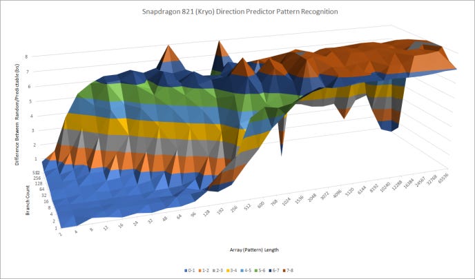
The Cortex A72 turns in a reasonable performance for an older, low power core. Compared to Kryo, it’s a bit better at recognizing long, repeating patterns. A72 also seems to have slightly more storage for branch history, letting it handle lots of branches before aliasing throws accuracy down the drain. That should give it an advantage over Kryo.

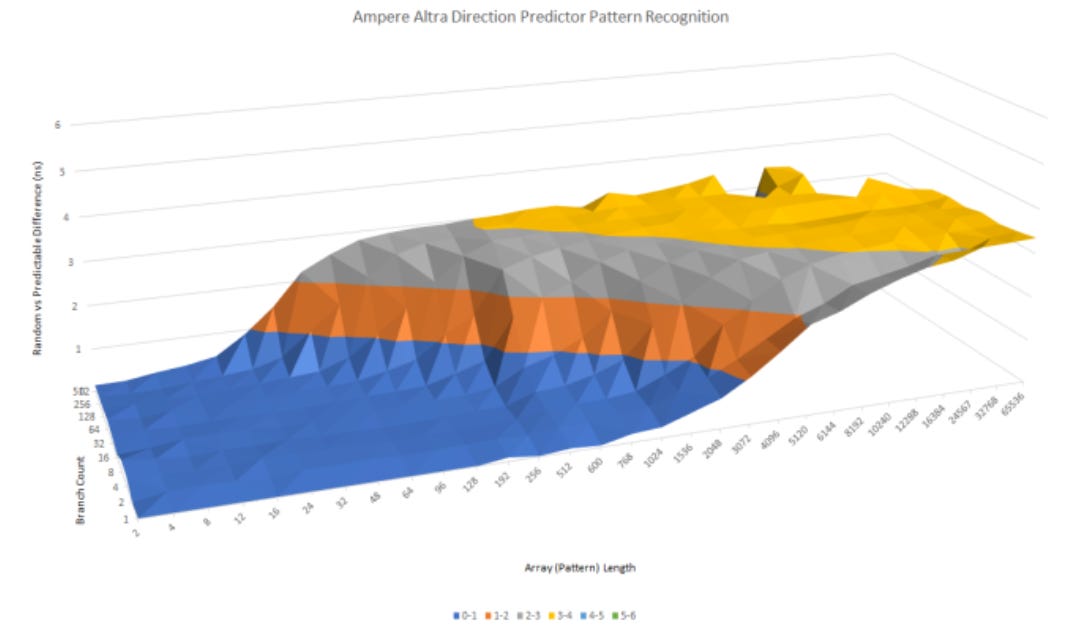
Cortex A72 falls short against ARM’s newer Neoverse N1 core, which replaces the A72 in AWS’s cloud offerings. N1 can recognize longer history lengths, and is slightly better at dealing with lots of branches. Branch mispredict penalties are also lower on N1, because N1 clocks up to 3 GHz on Oracle’s cloud.
Indirect Branch Prediction
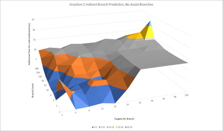
The A72 has a modestly capable indirect branch predictor for handling branches that hit multiple targets. We see a maximum of 256 targets (128 branches, two targets each) handled with relatively low latency per branch. For a single indirect branch, the A72’s indirect predictor can track at least 16 targets.
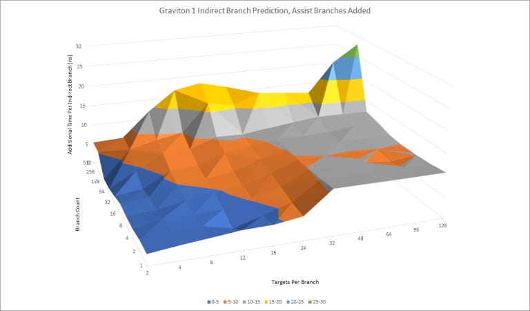
The A72’s indirect predictor also has a curious tendency to mispredict when there’s four or fewer branches in play, each with four or fewer targets. This is remedied if target selection correlates with nearby direct branches, indicating that A72’s target selection takes global taken/not taken history into account. A72 can clearly take an indirect branch’s local target history into account as well – it handles up to 16 targets for a single branch with no issues. But it’s bad at using local target history for short patterns, which is strange.
Return Prediction
Call (branch with link on ARM) and return pairs are a special case of indirect branches. Unlike other indirect branches, it’s easy to predict where a return will go by storing the call instruction’s address. For those, ARM has implemented a return address stack. Paul Drongowski estimates that it’s 8 entries deep, but from my test results, I believe it’s 31 entries:
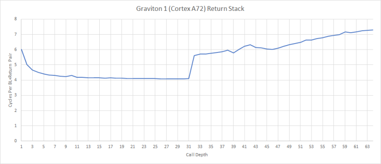
A72’s return stack is deeper than Kryo’s, which only has 16 entries.
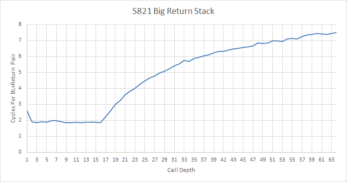
It’s also deeper than the return stack on contemporary Intel microarchitectures such as Haswell, which has 16 entries.
Branch Target Buffer
Now, let’s look at prediction speed for regular (direct) branches. To speed up branch prediction, branch targets are cached in a structure called the branch target buffer (BTB). The BTB lets a branch predictor tell the fetch unit where a branch will go, far before the branch instruction’s bytes have been fetched.
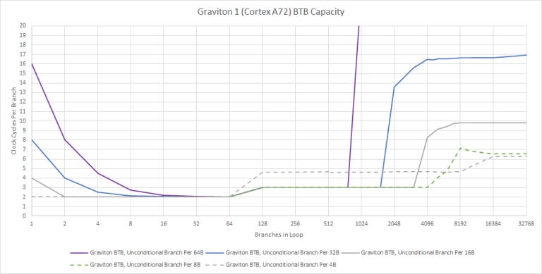
Our BTB capacity test gives weird results. According to Paul Drongowski, the A72’s BTB has varying capacity depending on branch distance.
Cortex-A72 allows split BTB entries, accommodating both near branches (small target address) and far branches (large target addresses). That’s why you will see the BTB capacity quoted as 2K to 4K entries. The A72 BTB can hold as a many as [sic] 2K large target address (far) and 4K small target addresses (near).
I’m not completely satisfied with that explanation. A72’s maximum BTB capacity certainly seems to be 4096 branches, with one branch every 8 bytes. That could correspond to the “near branch” BTB. The “far branch” BTB looks like it’s tied to the code cache. The maximum number of branches that A72 can track correlates perfectly with instruction cache capacity. Another possibility is that we’re just seeing instruction cache miss latency. In any case, A72 is unable to use its branch predictor for instruction prefetching. That makes instruction cache misses very expensive.
Speed-wise, A72’s BTB is unimpressive. It can’t do zero bubble branches at all. Even the 64 entry “micro-BTB” causes a frontend pipeline bubble after a taken branch, meaning that it has a latency of two cycles. The main BTB has three cycle latency. Loop unrolling is going to be pretty important for extracting maximum performance from the A72. But applications will have to be careful with that, because unrolling too much will increase code size and cause L1i misses.
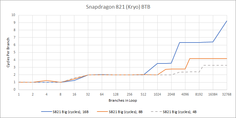
Qualcomm does better. Kryo has a smaller first level BTB with just eight entries, but can handle branches without pipeline bubbles. After that, it has a two level BTB tied to the instruction cache. Within 8 KB, branches are handled at a rate of one every two cycles. That matches A72’s much smaller micro-BTB in terms of speed, while having several times the capacity. Finally, there’s a 1-2 cycle penalty as long as the code fits within the 32 KB instruction cache. Overall, Kryo can track slightly fewer branch thanks to its smaller L1i. But for a lot of cases, it’s going to have faster branch performance than the A72.
Frontend: Fetch and Decode
Once the branch predictor has provided fetch targets, the frontend has to fetch the instruction bytes and decode them into an internal format. First though, it has to convert the virtual address provided by the branch predictor to a physical one. The Cortex A72 uses a 48 entry, fully associative instruction TLB to accelerate these address translations.
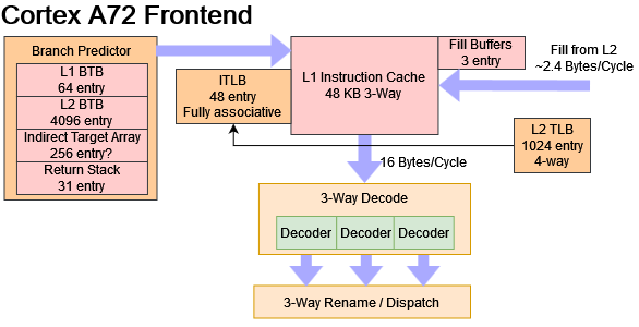
Then, the A72 checks its 3-way set associative 48 KB L1 instruction cache. The cache is connected to the fetch unit using a 128-bit bus, allowing it to deliver 16 bytes per cycle. To save power with sequential instruction accesses, A72 tries to only check L1i tags once for each 64 byte cache line. If the stars align (no taken branches in the cache line), A72 can make up to four sequential 16 byte instruction fetches with a single tag check:
if a cache read is sequential to the previous cache read, and the read is within the same cache line, only the data RAM way that was previously read is accessed.
For reliability the A72 protects the L1i’s contents with one parity bit per 16 bits of instruction data. The instruction cache’s tags are protected with two parity bits per tag. That lets A72 detect single single bit flips, but not correct them on the fly. On a parity error, “correction” is performed by reloading the line from L2. ECC isn’t necessary for the L1i, because it never has to hold modified data.
If there’s an L1i miss, the A72 goes to L2. Along with (obviously) requesting the cache line that generated the miss, the A72 also pulls in the next adjacent line. This is a pretty conservative prefetch strategy, but if A72’s BTB is tied to the L1i, there isn’t much choice. Fetching a pair of lines already pulls in 32 aarch64 instructions. There’s a good chance of a taken branch in those 32 instructions, which would make everything afterwards useless.
Contemporary high performance architectures like Sandy Bridge and Haswell decouple the BTB from the L1i, meaning the branch predictor can keep generating branch targets after a L1i miss. That scheme allows for better performance when an application’s code footprint doesn’t fit within L1i. But it’s more complicated to pull off, uses more power, and requires lots of memory level parallelism on the instruction side to be effective.
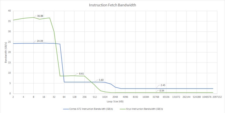
A72 lacks that kind of memory level parallelism. The L1 instruction cache has three fill buffers for tracking instruction cache refills, but tracking three L1i misses at a time isn’t enough to absorb L2 latency. So, we see low instruction fetch bandwidth from L2. Because aarch64 uses fixed length, four byte instructions, we can also show instruction fetch bandwidth in terms of instructions per clock (IPC):
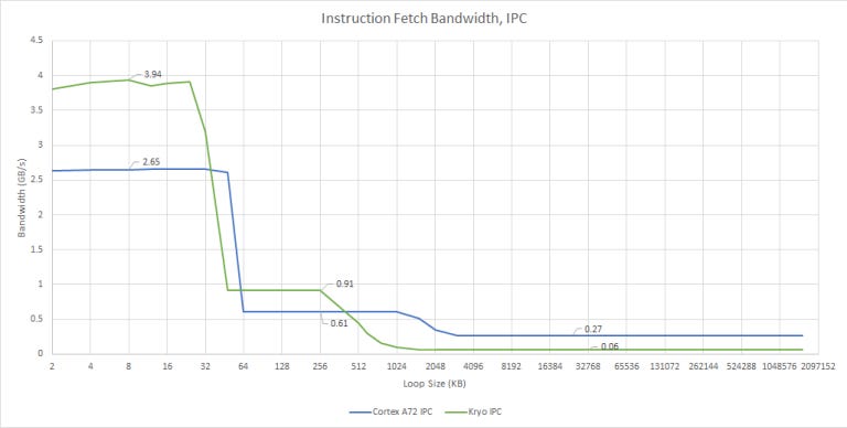
L2 fetch bandwidth is better on Kryo, but still bad in absolute terms. Both Kryo and A72 want applications with small code footprints, because instruction cache misses are very expensive on these low power architectures. Neither core can sustain even 1 IPC when running code out of L2, although Kryo gets close.
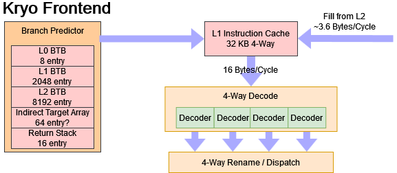
Compared to Kryo, A72’s frontend is weaker in most respects. The most obvious difference is that Qualcomm has a 4-wide decoder, while A72 can only decode three instructions per cycle. Kryo also fares slightly better when it has to fetch instructions from L2, and can handle taken branches with less latency. A72 does have a slightly larger instruction cache, but Kryo will somewhat offset that with higher associativity.
To reduce decoder latency and power, ARM predecodes instructions when they’re filled into L1i, and stores them in an intermediate format. That allows ARM to use much simpler decoders after L1i fetch.
After the frontend has fetched and decoded instructions, they’re sent to the renamer. There’s not much to say about the renamer in A72. It can’t eliminate dependent register to register moves. It can recognize that moving an immediate value of zero to a register is a zeroing idiom that breaks dependency chains, but that’s expected of any basic renamer anyway. The same applies to Kryo.
Backend: Out of Order Execution Resources
ARM has equipped the Cortex A72 with a modest set of instruction tracking resources, to let it search for instruction level parallelism past a long latency operation. Contemporary desktop CPUs have larger out of order engines, but A72 does have more reordering capacity than AMD’s Jaguar and Intel’s Silvermont. Compared to Qualcomm Kryo, A72 has similar reorder buffer capacity, but makes different tradeoffs with how specific resources are allocated.
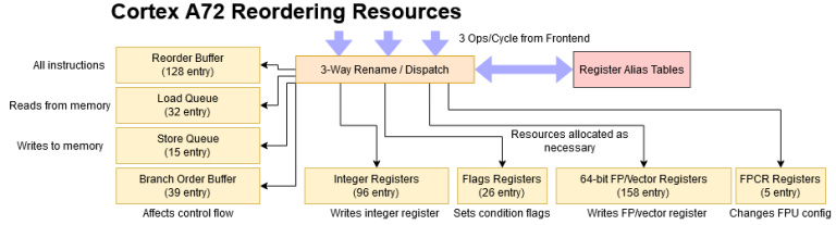
Cortex A72’s 128 entry reorder buffer (ROB) is large for a low power core. Unlike Zhaoxin’s Lujiazui, ARM uses separate register files instead of storing instruction results directly in the ROB. The integer register file allows 64 renames, meaning about half of the instructions in flight can produce an integer result. That ratio falls short of what we’ve seen in most other architectures, though it is slightly better than Golden Cove’s.
Surprisingly, the floating point register file is large enough to cover the entire ROB. That’s because the A72’s FP/vector registers are only 64-bit wide. 128-bit NEON vectors are handled by allocating multiple 64-bit registers; a single 128-bit vector result appears to consume five 64-bit registers. This explains why A72 needs so many 64-bit FP registers. It needs them to ensure adequate renaming capacity for 128-bit NEON code. As a side effect, A72 has incredible scalar floating point rename capacity for a core of its size, and only falls a bit short of Haswell in that respect.

Memory reordering resources are also a bit light on the Cortex A72. The load and store queues cover a fourth and eighth of the reorder buffer, respectively. Only the branch order buffer and renamed flag register file are proportionately sized, perhaps indicating a focus on handling branchy code.
ROB coverage isn’t the complete picture though. After all, the ROB might be oversized at very little cost to allow using all of the 64-bit FP registers, which were needed anyway to provide adequate renaming capacity for 128-bit vector instructions. So, let’s compare Cortex A72 against low power x86 cores:

In most areas, the Cortex A72 has more reordering capacity than Jaguar and Silvermont. It should therefore be better at absorbing memory latency, unless there’s a lot of 128-bit operations or stores. Combined with its wider core width, A72 should offer more performance per clock than AMD and Intel’s low power architectures from a couple years before. From that perspective, the Cortex A72 is exactly where it should be.
Notes
Very inconsistently, Haswell can give a single thread about 148 integer register renames, indicating that it doesn’t need to store architectural state for both threads in the register file.
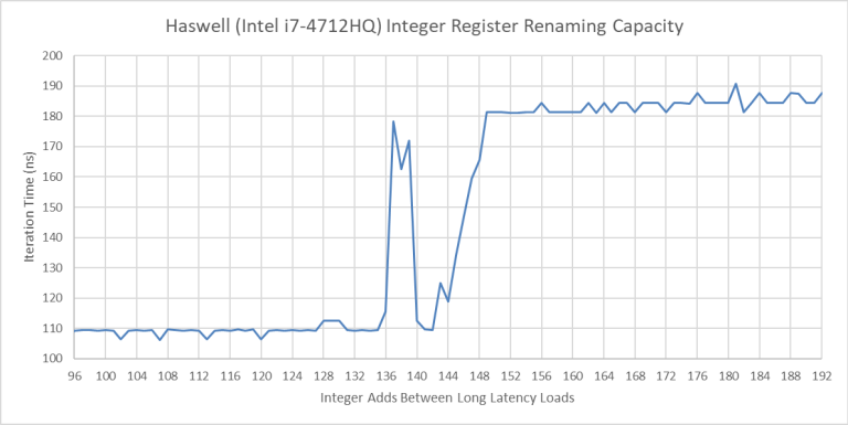
The spike between 136 and 144 is reproducible. Intel documents 168 integer registers. So it makes sense that 136 registers are available for renaming, with the other 32 used to hold non-speculative state for both threads.
2. Silvermont has 32 entry rename buffers, with speculative results copied into separate architectural register files at retirement. It therefore has 32 registers available for renaming.
Backend: Scheduling and Execution
ARM uses a distributed scheduler with Cortex A72. Each port has its own issue queue, which simplifies scheduler design – each queue only has to be searched for one execution unit, and only one micro-op needs to be read out from each queue per cycle. In contrast, Qualcomm takes a hybrid approach with Kryo. The integer schedulers are somewhat unified, in a layout that slightly resembles Zen 3’s, while the other schedulers are mostly distributed.
Integer Execution
Cortex A72 has two simple ALU pipes, and separate pipes for complex integer operations and branches. Each integer pipe has an 8 entry issue queue, while the branch pipe has a 10 entry queue. The core can therefore have up to 34 micro-ops waiting for an integer execution unit.
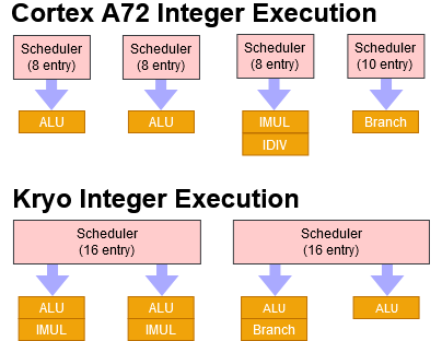
Kryo has 32 total scheduler entries, but in a more flexible arrangement. While it’s not completely unified, there are more scheduler entries available for every type of integer instruction. The most basic and common integer instructions can use all 32 entries, compared to 16 on A72. Kryo can have 16 un-resolved branches in flight, while A72 can only have 10. Integer multiplies are in a similar situation: A72 can give them eight scheduling entries in a dedicated queue, while they get 16 entries on Kryo’s semi-unified scheduler.
Qualcomm has also equipped Kryo with a lot more integer throughput. It has four basic ALUs, compared to two on A72. Unusually, Kryo also has two integer multiply units. They don’t seem to be fully pipelined, and achieve 1.25 multiplies per clock on average. But that’s still better than A72’s single multiply per clock. Integer multiplication latency is five cycles on both Kryo and A72.
Obviously, Kryo’s integer side offers higher performance, at the cost of higher complexity and probably higher power consumption. A72’s smaller, single-ported issue queues and dedicated pipelines indicate that ARM’s aiming for a simpler, lower power design.
Floating Point and Vector Execution
The Cortex A72 has two pipelines for handling floating point and vector operations, each fed from a modestly sized 8 entry issue queue. Vector throughput is modest, since most 128-bit instructions are executed at half rate. Packed 128-bit integer additions are a notable exception, and execute at full rate on both pipelines. Unlike AMD’s Zen and Intel’s Gracemont, instructions with vector lengths longer than that of the execution units are not split into two micro-ops. A72’s vector execution scheme looks a bit like the one in Intel’s Pentium 4, where a 128-bit instruction is kept as a single micro-op, and sent to the execution unit twice.

Kryo’s vector execution engine is more ambitious, with almost double the scheduling capacity and 128-bit execution units all around. To summarize:

A72 is quite competitive against Kryo for scalar floating point instructions. Both of A72’s FP pipes can handle common scalar FP operations every clock, letting it match Kryo’s FADD throughput while beating it when FMULs are involved. Kryo, meanwhile, offers better execution latency.
For vector floating point instructions, Kryo generally has an advantage. Its 128-bit FPUs offer superior throughput and lower latency. The same applies to vector integer math. A72 brings dual 128-bit vector adders, but Kryo can do the same with lower latency. With vector integer multiples, Kryo provides better throughput at equal latency.
While Qualcomm tried to pack some vector processing punch into a mobile core, ARM focuses on the basics and power efficiency. Scalar floating point performance is probably important for Javascript, where the ubiquitous “number” type is a 64-bit floating point value. That may have driven ARM’s decision to duplicate 64-bit FP units across two pipes. Vector floating point throughput probably isn’t critical on a mobile core, where computationally heavy tasks are either offloaded to specialized IP blocks, or sent off to a remote server. Still, A72 does a credible job with its vector and FP execution side. Earlier low power cores like Intel’s Silvermont also execute some packed 128-bit FP instructions at half rate. Kryo’s setup can therefore be considered above average, while A72’s is about average.
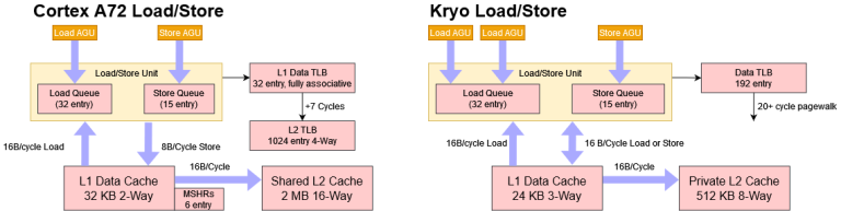
Address Generation and Load/Store Unit
Cortex A72 has two address generation unit (AGU) pipelines. One handles load operations, while the other handles stores. Both have their own 8 entry issue queue to buffer micro-ops waiting to execute.
Kryo’s AGU setup is more flexible. It can handle two loads per cycle, or a load and a store. And, Kryo has a bit more scheduling capacity than A72. For perspective, AGU scheduling capacity stood out when we looked at how Zen 2’s scheduling resources held up in Cinebench R15:

AGU scheduler size isn’t a huge issue, but Zen 2 has an even larger and more flexible AGU scheduler layout than Kryo. A72’s weaker AGU setup will probably cost it a bit of performance. On the other hand, dedicated load and store schedulers should simplify renamer logic, because there’s only one way to allocate backend resources for any memory operation. Kryo would need extra logic to select which port to bind load operations to.
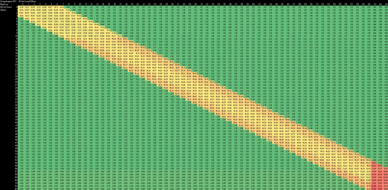
Once addresses are generated, the load/store unit has to check whether a memory load overlaps an older in-flight store. If it does, the store’s data is “forwarded” to the load. The A72 can do this with a latency of 7 cycles. Its store forwarding mechanism is able to maintain this latency even when the load only partially overlaps the store. It does suffer an extra cycle or two of latency if both the load and store cross a 16 byte boundary and the load only partially overlaps the store. If both the load and store cross a 64 byte cache line boundary, there is an extra 2-3 cycle latency penalty. Amazingly, store forwarding is “free” if a 32-bit load gets its result from the upper half of a 64-bit store.
This robust store forwarding behavior might be possible because A72 doesn’t do memory dependence speculation. Loads are stalled until the core can determine the addresses of all prior stores. That means when a load executes, it can check all prior stores and know with certainty whether forwarding is required.
For independent memory operations, stores on A72 run at half rate if they cross a 8 byte boundary, and the same applies to loads if they cross a 64 byte cache line boundary.
Kryo’s load/store unit also has robust detection of loads that depend on prior stores. Like A72, Kryo’s store forwarding succeeds for all cases where the load is contained within the store, but has a very high latency of 15-16 cycles. If the load partially overlaps the store, an extra cycle is needed. This high store forwarding penalty even in easy cases suggests Kryo handles memory dependencies very late in its load/store pipeline.
If the coloring is changed to show differences at lower values, we can see that Kryo takes an extra cycle if a load and store both touch data in the same 4 byte aligned region, even though they’re independent. Kryo’s probably doing a fast store forwarding check at 4 byte granularity (only comparing the high address bits), then taking an extra cycle to do a more thorough check if the first check indicates a possible store forwarding opportunity.
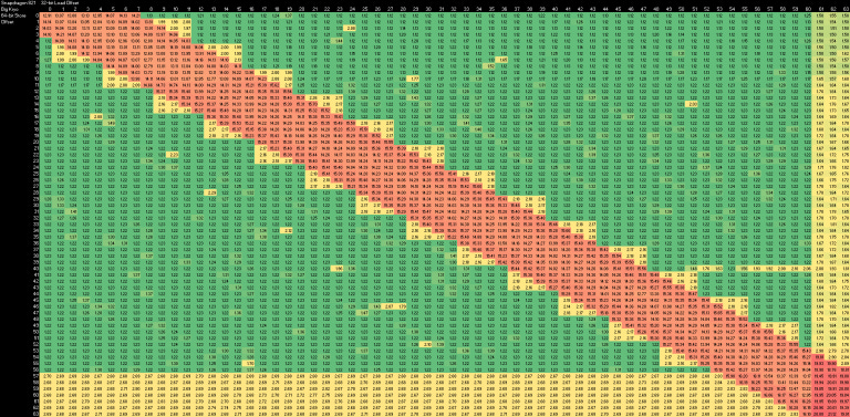
Unlike A72, Kryo doesn’t have any extra costs when stores cross 8 byte boundaries. We only see penalties for accesses that span 64 byte cache lines. Kryo’s memory dependence handling has some parallels to that of last-generation Intel big cores, from Sandy Bridge to Skylake, but with far higher store forwarding latency.
We’ll cover memory bandwidth in more detail later. In summary though, A72 can execute a 128-bit vector load every cycle. 128-bit vector stores execute at half rate, indicating that A72’s L1 data cache only has a 64-bit write path. From our Kryo testing, Qualcomm’s core can execute 1.26 vector loads per cycle, while vector stores execute at one per cycle.
Cortex A72’s Memory Subsystem
With every CPU generation, DRAM performance falls further behind core performance. That makes caching strategy very important. A cool core design is useless if you can’t feed it.
What limits computer performance today is predictability, and the two big ones are instruction/branch predictability, and data locality.
Since we covered branch prediction early on, let’s have a look at A72’s caches, which exploit locality in data accesses. And of course, we’ll look at DRAM performance too.
Latency
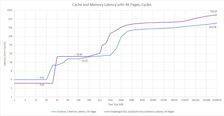
A72 has a 32 KB, 2-way set associative data cache with 4 cycles of latency. Strangely, we see higher latency than expected when randomly pointer chasing in a region larger than 16 KB. With huge pages, we see 4 cycle latency throughout the 32 KB L1D, as expected. ARM’s Cortex A72 Technical Reference Manual clearly states that the core has a “32-entry fully-associative L1 data TLB with native support for 4KB, 64KB, and 1MB page sizes”. We shouldn’t be seeing any L1 DTLB misses before 128 KB, so the higher L1D latency past 16 KB is hard to explain.

In L2 sized regions, we see just above 9 ns of latency, or 21 cycles at 2.3 GHz. That level of latency may seem rather high for people used to looking at desktop systems, as it’s rather close to L3 latency on Haswell and Zen 2. But it’s typical for low power designs with a shared L2. For example, Tremont has a 19 cycle L2, with actual latency lower because of higher clocks.
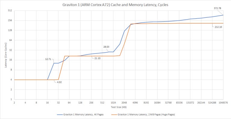
Past 128 KB, we start missing the L1 DTLB. Hitting in the 1024 entry, 4-way set associative L2 TLB adds another seven cycles of latency, or about 3 ns. Main memory latency on Graviton 1 is just above 92 ns. Using 4K pages brings that to a staggering 162 ns, indicating that A72’s pagewalk performance is poor. The core itself isn’t completely to blame, because loading page table entries out of the slow L2 (or even memory) will introduce a lot of latency.
Qualcomm’s Kryo approaches caching differently. It has a smaller but faster 24 KB, 3-way L1D with 3 cycle latency. Virtual to physical address translations are cached by a single level 192 entry TLB in an all-or-nothing approach.
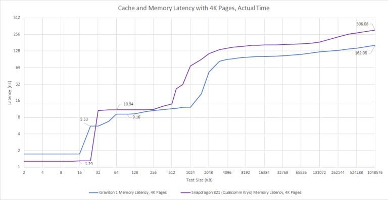
Each Kryo core has a private 512 KB, 8-way L2 cache (256 KB on small Kryo cores). L2 latency is brutal, at 25 cycles on big cores and 23 cycles on the little ones. After L2, Kryo accesses DRAM with GPU-like latency. Qualcomm has done a horrifying job with Kryo’s memory subsystem, and that’s going to limit the core’s potential if workloads don’t fit in L1.
Arm lets implementers configure L2 cache size from 512 KB to 4 MB. In theory, an implementer can pick the smallest cache size and end up in a similar situation to Qualcomm. Thankfully, Graviton 1 hasn’t done that.
Bandwidth
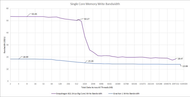
Cortex A72 can do a single 128-bit load per cycle, meaning its bandwidth looks rather low next to contemporary desktop cores. Strangely, read bandwidth drops after 16 KB, even though the L1 data cache should be 32 KB in size.
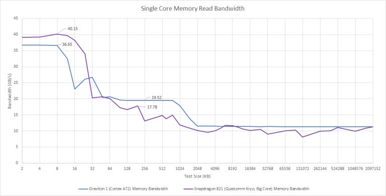
From L2, Cortex A72 can read in just above 8 bytes per cycle. The core probably has a 16 byte per cycle path between L1 and L2, but isn’t using it very efficiently. But ARM isn’t doing a bad job here. Qualcomm is worse even though their L2 is smaller and isn’t shared.
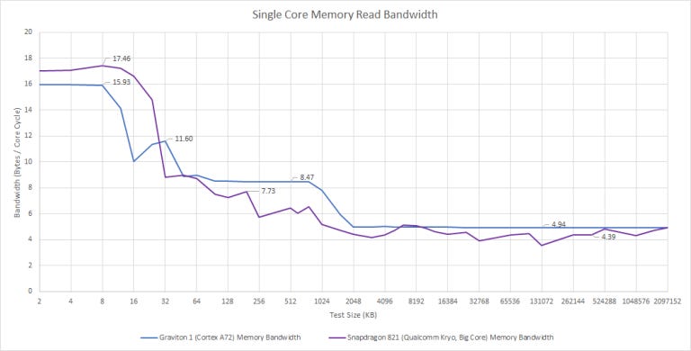
Graviton 1’s write bandwidth is lower than read bandwidth. That’s understandable because reads are more common than writes. Kryo on the other hand is crazy, it has better write bandwidth. That may be because write latency doesn’t matter. Once a core retires an instruction that writes to memory, it can probably stop tracking it once the write data has been handed off. With reads, the core has to track the outstanding memory request until the read completes.
System Architecture and Bandwidth Scaling
Graviton 1 arranges Cortex A72 cores into clusters of four. Each cluster has a 2 MB L2 cache, shared by all four cores. An “a1.metal” AWS instance has four of these clusters, for 16 total cores.
Bandwidth Scaling, Big Picture
Like Tremont, L2 bandwidth doesn’t scale to more than two cores. Unlike Tremont, which can load 32 bytes per cycle from the L2 with all four cores active, Graviton 2’s L2 is stuck at just under 16 bytes per cycle. That’s 4 bytes per core cycle, which could be a limitation for workloads that don’t fit in L1D.
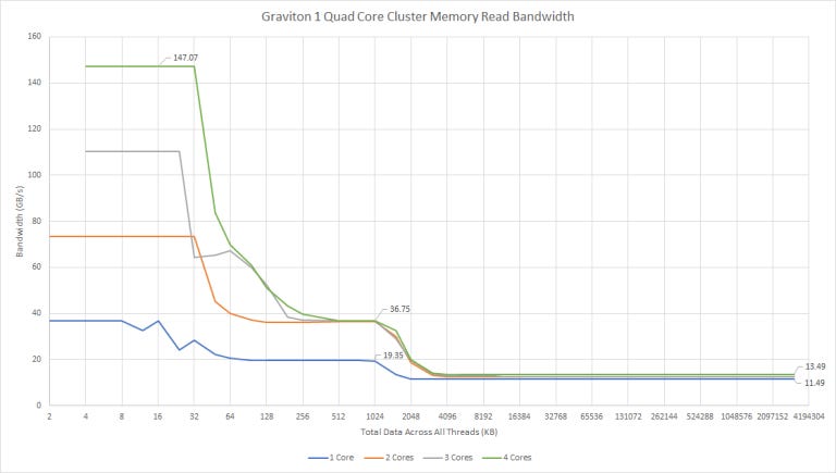
Memory bandwidth also sees very little scaling within a cluster. With all cores loaded, we get 13.5 GB/s of read bandwidth – not very impressive. We could be limited by the off-cluster interface. Arm’s technical reference manual states the L2 has 20, 24, or 28 fill/eviction queue entries to handle misses. That may not be enough parallelism to absorb memory latency.
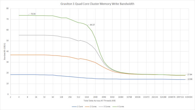
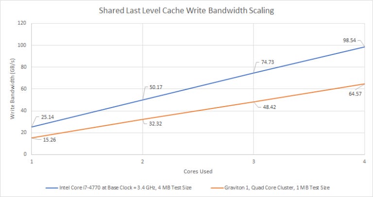
Write bandwidth is worse from L1D and L2 for a single thread, but surprisingly scales better as more cores are loaded. We can write just under 32 bytes per cycle to L2. Bandwidth doesn’t increase further if we mix reads and writes, so there could be a single 32 byte wide path to L2 that’s used inefficiently for reads, or a 16 byte wide read path and 32 byte wide write path. DRAM bandwidth is also better with stores, again indicating that the core doesn’t have deep enough queues to absorb memory latency for reads.
Shared L2 Performance, in Context
To put Graviton’s intra-cluster interconnect and caching performance in context, let’s look at a contemporary design (Haswell) that uses a ring bus to provide a unified last level cache for four cores.
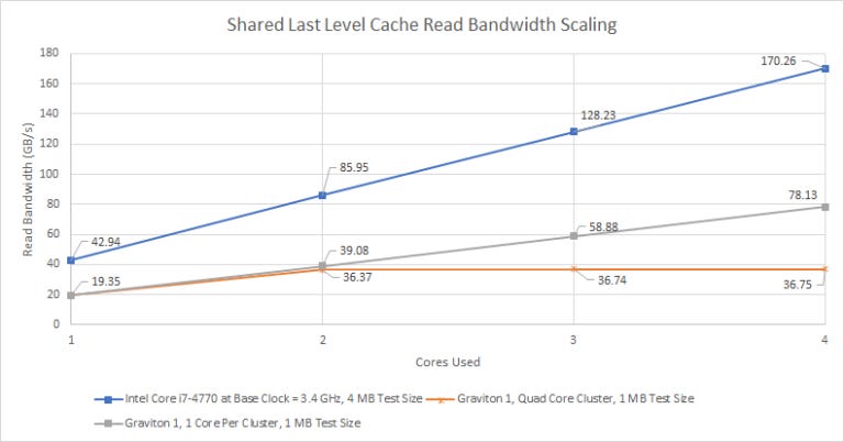
Next to Haswell’s L3 with a ring interconnect, Graviton’s shared last level cache starts with low bandwidth for a single core, and doesn’t scale. Even if we normalize for clock speed, Graviton’s intra-cluster interconnect and cache design fall behind.
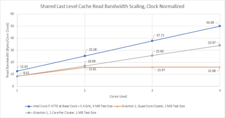
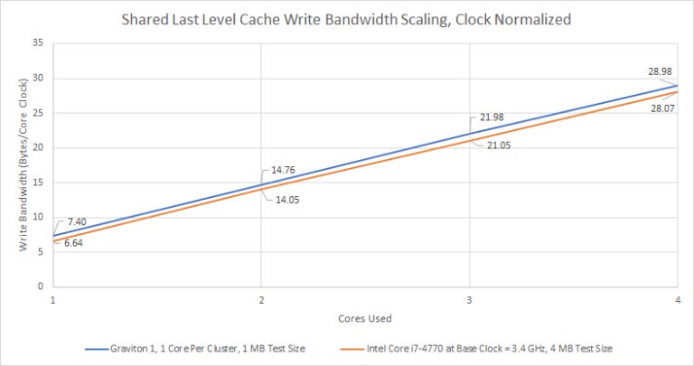
As we saw before, Graviton’s write bandwidth scaling is far better. Absolute numbers are low, because Graviton isn’t designed to hit high clock speeds like Haswell.
If we normalize for clock speed, Graviton puts in a pretty respectable performance:
Graviton’s L2 cache isn’t quite as bad as read bandwidth numbers would suggest. But as we mentioned before, load instructions are more common than stores. When we analyzed two workloads, 7-Zip compression and libx264 video encoding, the load-to-store ratio was 3.4:1 and 2.3:1, respectively. In addition to data accesses, the L2 cache also handles instruction cache refills. Those are always reads, so the read-to-write ratio at L2 is likely even more skewed in the ‘read’ direction. So while the better write bandwidth scaling is certainly nice to see, Graviton will likely still have L2 cache bandwidth problems.
DRAM Bandwidth Scaling
With all four cores loaded in a cluster, we get about 13.5 GB/s of read bandwidth. If we load one core in each of the four clusters, read bandwidth increases to over 36 GB/s, suggesting limitations in the interface between the cluster and the chip-level interconnect. Read bandwidth doesn’t increase further if more cores are loaded. Write bandwidth with all 16 cores loaded is just above 27 GB/s.
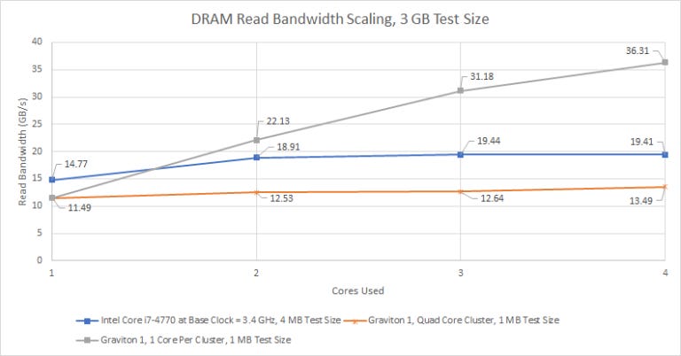
So, Graviton has a reasonably beefy memory subsystem. It’s probably some kind of quad channel setup with fast DDR3 or slow DDR4. In any case, Annapurna Labs has equipped Graviton with a lot more memory bandwidth than what you’d see in a 2013 era desktop system with dual channel DDR3-1333.
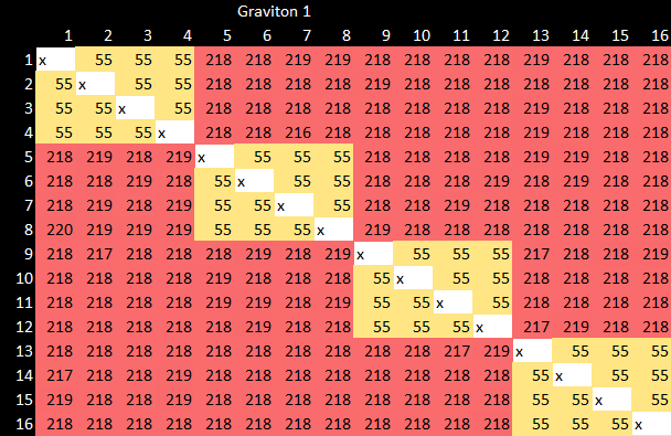
Cache Coherency Latency
Graviton 1 handles cache coherency at two levels. Within a cluster, the L2 cache controller maintains a “snoop tag” array that holds a copy of each core’s L1 data cache tags. If a request hits the “snoop tag” array, its data gets pulled from the corresponding core’s L1.
This mechanism handles intra-cluster coherency with moderate latency. It’s not as fast as a tightly coupled ring interconnect, but it’s perfectly acceptable.
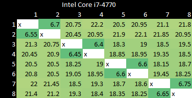
Here’s Haswell for comparison. Core to core lock latency is very low, thanks to a high speed ring bus tightly coupled to the cores and L3 cache.
Across clusters, Graviton 1 is much slower. Over 200 nanoseconds is basically cross-socket latency for server chips. In fairness, Qualcomm does worse:
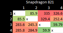
I suppose cache coherency wasn’t very well optimized for mobile chips, and that weakness carries over in server designs. We don’t think this core to core latency has a significant impact on performance, so we’re not going to attach too much importance to this. But it is interesting to see the system topology.
Final Words
ARM’s Cortex A72 is a small, but competent low power core that has proven itself to be capable enough for a wide range of applications where the CPU isn’t expected to do heavy lifting. The core’s biggest strength is its out-of-order execution capability with deep reordering capacity. A relatively large 48 KB L1 instruction cache provides an advantage as well.
Caching is A72’s biggest weakness. In Graviton, four A72 cores share a L2 cache in a cluster. This cache is small at 2 MB and suffers from high (21 cycles) latency. Bandwidth is low, as the entire cache seems to have a single 16 byte/cycle (128-bit) interface shared by all four cores. Because the L2 is responsible for handling all L1 data and instruction cache misses, its small size and poor performance doesn’t do A72 any favors. The memory hierarchy beyond L2 is weak as well. A cluster of four A72 cores is limited to about 13.5 GB/s of DRAM read bandwidth, suggesting a narrow link between each cluster and the rest of the SoC.
Other limitations exist of course, but these are mostly inherent to the core’s low power designs and more excusable. For example, vector execution performance was sacrificed. A72’s execution units and registers are 64-bits wide, meaning that 128-bit NEON operations consume multiple registers and suffer from lower reordering depth limits. But that’s not much of a problem if the core isn’t meant to do heavy number crunching in the first place. A72’s distributed schedulers are small. These are probably cheap to implement in terms of die area and power, but will likely fill quickly. Still, a larger scheduler setup may have been inappropriate given the core’s low power goals.
For cell phones, hobbyist single board computers, and networking devices that need a CPU of some kind to handle management functions, A72 is perfectly adequate. For servers, A72’s sub-par caching and memory setup are likely to hold the core back.
If you like our articles and journalism, and you want to support us in our endeavors, then consider heading over to our Patreon or our PayPal if you want to toss a few bucks our way. If you would like to talk with the Chips and Cheese staff and the people behind the scenes, then consider joining our Discord.