
ARM’s Neoverse N2: Cortex A710 for Servers

ARM’s Neoverse N1 was based on ARM’s Cortex A76 mobile core, but enhancements like instruction cache coherency and 48-bit physical addressing made it usable in servers. The result was quite successful and gave ARM a foothold in the server marketplace. Graviton 2 implemented Neoverse N1 on Amazon Web Services, while Ampere Altra found a place in Microsoft Azure and Oracle Cloud.

Neoverse N2 looks to continue that success. Thanks to our team member Titanic, we had brief access to an octa-core Alibaba Yitian 710 cloud instance. The Yitian 710 uses ARM’s Neoverse N2 cores, letting us examine a real world Neoverse N2 implementation. A full Yitian 710 chip has 128 cores running at up to 3.2 GHz, and contains 60 billion transistors. To feed the cores, Alibaba uses an eight channel DDR5 setup and 96 PCIe 5.0 lanes. We can’t evaluate the full chip, but microbenchmarking an individual core shows characteristics extremely similar to that of the Cortex A710. These similarities persist down to an ALU count discrepancy, where only three ALU pipes could handle the most common operations like integer adds and bitwise operations.
We’re going to briefly evaluate the basic A710/Neoverse N2 core, and compare it with Zen 4. AMD’s Zen 4 is an interesting comparison because it has a density-focused variant (Bergamo) that trades L3 cache capacity and clock speeds to reduce area usage. Intel’s Sapphire Rapids is also a notable competitor, but focuses more on per-core performance than density.
Then, we’ll pivot to the differences between A710 and N2. Most differences relate to the all-important cache hierarchy, though there are a few minor core changes.
Block Diagram
Neoverse N2, is a 5-wide out-of-order core that looks mostly identical to Yitian 710. It combines modest reordering capacity with a relatively oversized scheduler and a modern branch predictor. According to ARM, N2 has a 10 cycle pipeline. That figure probably corresponds to minimum branch mispredict penalty when the correct target is found in the micro-op cache. For comparison, Zen 4 has a 11 cycle minimum mispredict penalty.
I didn’t have time to microbenchmark everything on a cloud instance, so I focused on undocumented structure sizes and checking those against results on A710. Where ARM did publish figures, I’m using those instead of estimating based on test results.
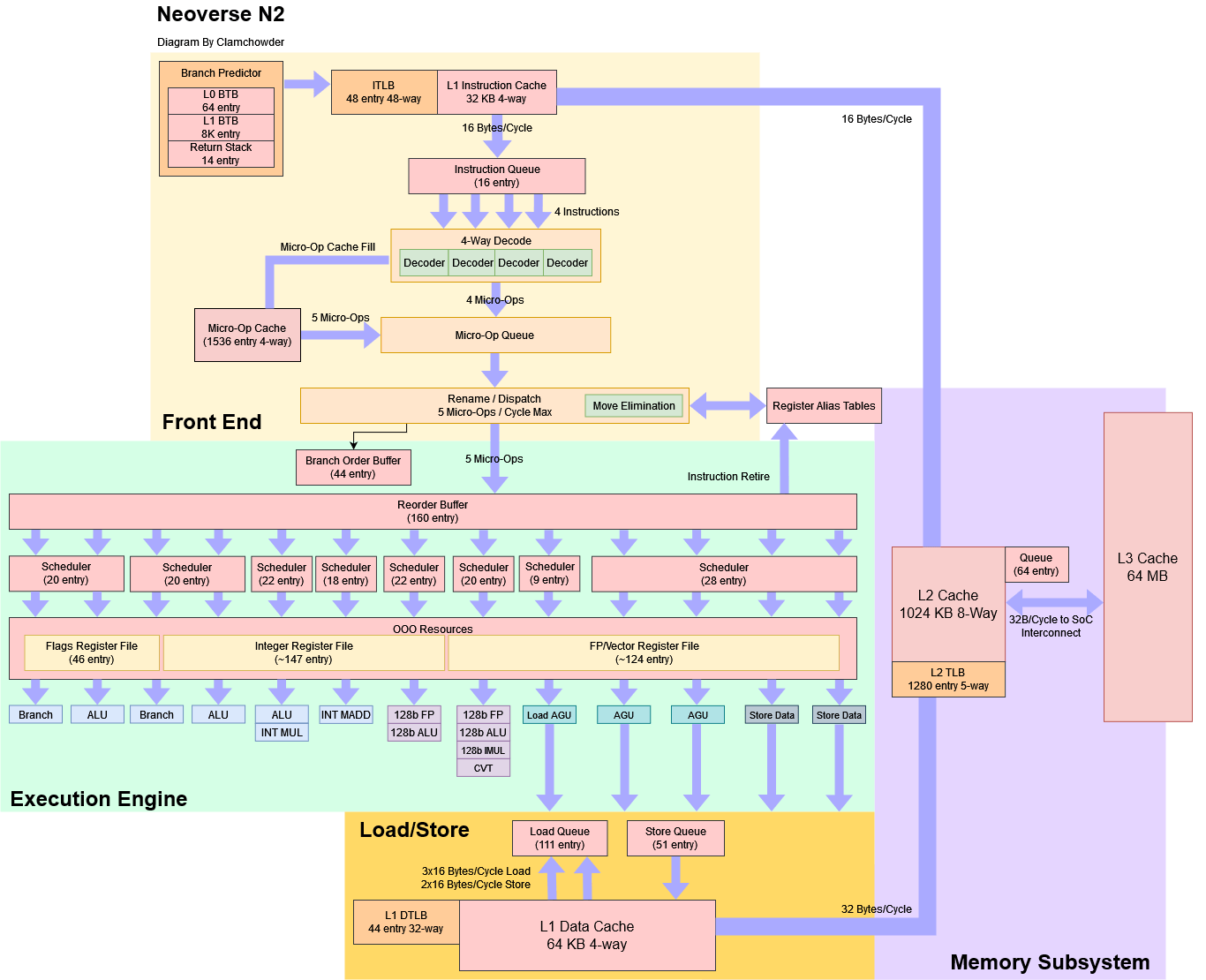
For example, BTB test results on the Yitian 710 look identical to those from the A710, but ARM states there’s a 64 entry micro-BTB backed by an 8K entry BTB. This setup is plausible as A710/N2 can sometimes handle more than one taken branch per cycle with less than 64 branches in play, though I originally discounted this as measurement error. The 8K main BTB figure is also plausible, though I didn’t see a significant increase in taken branch latency until test sizes exceeded 10K branches.
Compared to Zen 4
Zen 4 is a 6-wide core that’s larger in pretty much all aspects. Its server form is very closely related to its client one, but features 52-bit physical address support, up from 48 bits in client versions. Zen 4 is closely related to AMD’s prior Zen 3 architecture, but has received upgrades throughout the pipeline and introduces AVX-512 support.
Branch Prediction
Neoverse N2’s branch predictor is both modern and capable, but falls a step behind Zen 4’s. AMD has invested a lot of core area into the branch predictor since Zen 2, and has one of the fastest and most accurate predictors. N2 takes a more conservative approach in order to maximize density.


I expect N2 to have slightly worse prediction accuracy. But N2 can compete quite well if branches are predictable, thanks to its fast, high capacity BTBs. Its ability to handle 2 taken branches per cycle can let it get through branchy code faster than Zen 4 can, as long as branch footprints are small.
Execution Engine
Neoverse N2 doesn’t have anywhere near as much reordering capacity as Zen 4. With a 160 entry ROB and approximately 147 integer registers (of which 116 are available for speculative renaming), N2 sometimes looks like Sandy Bridge. For comparison, Zen 4 has a 320 entry ROB and 224 integer registers.
However, ARM has invested in other areas to get the most of its ROB capacity. After all, more ROB entries aren’t very useful if another resource is exhausted first and forces the renamer to stall before the ROB is full. Neoverse N2’s load/store queues are not much smaller than Zen 4’s. And its scheduler layout is especially competitive.
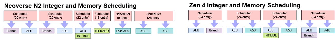
Zen 4 has a slightly more flexible scheduler layout thanks to a semi-unified design. Each operation type has multiple 24-entry scheduler queues to choose from. N2 is not far behind. Integer operations also enjoy ample scheduling capacity on ARM’s core. Memory accesses don’t compete with ALU operations for scheduler entries unlike on Zen 4, so the matchup will probably be quite close in practice.
Execution unit count is far less important than keeping the execution units fed, but on the execution throughput front, the two architectures are well matched. Both can resolve two branches per cycle. Neoverse N2 has an additional port for integer multiplies, while Zen 4 has one more general purpose ALU port. For memory accesses, the two architecture are largely equivalent. Zen 4 and N2 can handle three accesses per cycle, two of which can be stores.
Overall, Neoverse N2’s integer side is well done, with excellent scheduling capacity and enough execution throughput. I feel like N2 could use more register file and ROB capacity. Other core resources are enough to make good use of a 200+ entry ROB. And as we’ll see later, N2 has to hide a lot of latency if it fetches data from L3.
Floating Point and Vector Execution
Due to a testing screwup, this section has been revised.
Zen 4 and Neoverse N2 both introduce vector extensions over their predecessors. N2 gains SVE support, while Zen 4 is the first AMD core to support AVX-512. Unlike Intel, ARM and AMD did not increase execution unit width or port count to go with the new instruction set support.
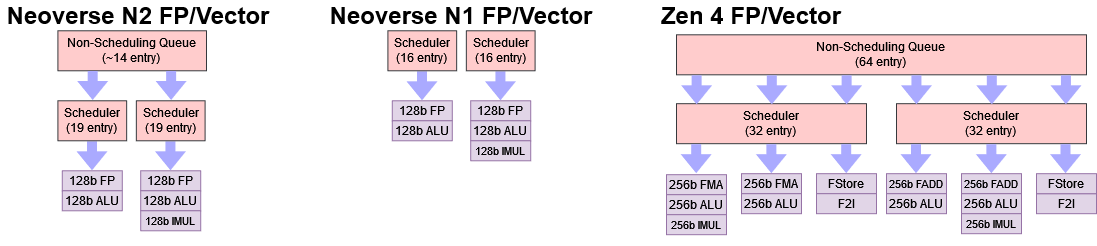
Execution port layout has not changed between Neoverse N1 and N2. There are still two pipes feeding 128-bit execution units. Scheduler capacity has gone up, so N2 has a better chance of smoothing out temporary spikes in demand for floating point or vector throughput. However, N2 combines a modest increase in scheduler capacity with a non-scheduling queue (NSQ). The NSQ lets non-FP operations get into their respective schedulers even if the FP schedulers are full. Applications rarely push execution units at full tilt, so just an increase in scheduler capacity could give N2 a good boost in FP vector performance.
If we consider when products implementing the cores became widely available, N1 was roughly contemporary with Zen 2, and N2 is roughly contemporary with Zen 4. AMD made substantial progress on the vector/FP side within that time. Compared to Zen 2, Zen 4 has a better execution port layout that takes pressure off Zen 2’s heavily used FADD/FStore pipe. Alongside that, Zen 4 nearly doubles FP scheduler capacity. ARM’s changes are minor in comparison.
In contrast, ARM’s changes focus on letting the core extract more instruction level parallelism around short sequences of FP or vector instructions. The non-scheduling queue lets the core keep around 52 incomplete FP/vector instructions in flight, or up to 30 for a single port. AMD is still better for FP and vector workloads thanks to its much larger schedulers and larger non-scheduling queue, along with 256-bit vector execution. However, ARM should be commended for providing a significant upgrade over Neoverse N1. Even if the execution port layout has not changed, they are much better supported.
Changes from Cortex A710
Clock Speeds
Cloud providers prefer consistent performance, which dictates capped or locked clock speeds. In the Yitian 710 instance we had access to, the N2 cores ran at a locked 2.75 GHz with no measurable boost delay coming from idle. Alibaba claims the chip can reach 3.2 GHz, but production instances might be set to a lower clock speed to improve yields and keep power consumption in check.
Neoverse N1 was in a similar situation. Several cloud providers opted for 3 GHz Ampere Altra SKUs, even though 3.3 GHz SKUs existed. As of August 7, 2023, Ampere no longer advertises frequencies above 3 GHz. So far, Alibaba’s Yitian 710 is the only Neoverse N2 implementation we’ve been able to test. Seeing how other N2 implementations clock will be quite interesting.
Address Translation
When running under modern operating systems, programs use virtual addresses to access memory. The operating system sets up page tables that map virtual addresses to physical addresses. Every memory access requires address translation, and CPUs cache these translations because traversing the page tables would turn a single program memory access into several dependent accesses under the hood.
Cortex A710 appeared to be optimized for smaller memory footprints. Its L1 DTLB was quite small with only 32 entries. DTLB misses could be absorbed by a 1024 4-way L2 TLB, but that is also small compared to the L2 TLBs found in Intel and AMD’s CPUs. Neoverse N2 targets somewhat larger memory footprints with a 44 entry DTLB, backed by a 1280 entry 5-way L2 TLB. That makes it similar to N1, which has identical L2 TLB capacity and just a slightly larger 48 entry L1 DTLB.

Neoverse N2 thus continues a trend of having worse TLB coverage than contemporary Intel and AMD cores. Both x86 manufacturers have been slowly but steadily increasing L2 TLB coverage, while L1 TLB size has stayed around 64 entries. Zen 4 has exceptional TLB sizes, with a 72 entry L1 DTLB and a 3072 entry L2 TLB. On top of that, Zen 4 uses a separate 512 entry L2 iTLB on the instruction side, increasing L2 TLB coverage when code and data aren’t in the same pages.
Bigger Physical Address Space
Besides increasing TLB capacities, ARM has also augmented them to support 48-bit physical addresses. A710’s 40-bit physical addressing could only address up to 1 TB of memory, which is inadequate for servers. N2 therefore gets 48-bit physical addressing support, letting it address up to 256 TB of memory.
Again, this change parallels the one from Cortex A76 to Neoverse N1. A76 supported 40-bit physical addressing, and N1 brought that up to 48 bits. And again, x86 systems are a step ahead. Genoa (Zen 4 server) and Intel’s Ice Lake use 52-bit physical addressing, letting them address 4 PB of memory. Today, such memory capacity is unthinkable for a single server, but 52-bit addressing can be useful for very large shared memory systems. ARM has no ambitions to put cores into such systems, so 48-bit addressing is adequate.
Cache Setup
Neoverse N2 has a different set of cache configuration options compared to its mobile cousin, A710. Generally, N2 aims for higher cache sizes, making it better suited to tasks with large memory footprints.

To start, all N2 cores get 64 KB L1 caches. This is a very good move from ARM, as 64 KB caches tend to have significantly higher hitrates than the 32 or 48 KB ones found on recent x86 CPUs. I wish AMD would bring back the 64 KB L1 caches they used on the K10-based Phenom and Opteron CPUs.
N2 also gets optional hardware instruction cache coherency. ARM recommends enabling it on systems with a lot of cores because broadcasting software-issued instruction cache invalidates would not be scalable. To implement instruction cache coherency, ARM makes the L2 cache inclusive of L1i contents. Then, I assume the L2 becomes exclusive of L1 data cache contents, ensuring that data writes will never cause a L1d hit when the address is in L1i. Finally, a read-for-ownership will evict a line from L2 caches in all other cores, which automatically causes L1i invalidates and prevents L1i caches from holding stale data.
ARM recommends configuring the core with 1 MB of L2. A 512 KB L2 would spend 1/8 of its capacity duplicating L1i contents to ensure L1i coherency, and a 256 KB L2 would be a really bad idea (likely why ARM doesn’t even allow it as an option). Thankfully, going to 1 MB of L2 capacity doesn’t cost any extra latency. Just as with A710’s 512 KB L2, getting data from L2 takes 13-14 cycles. Ampere Altra and Zen 4 have similar cycle counts for L2 accesses, though Zen 4 enjoys an actual latency advantage thanks to higher clock speeds.

A larger L2 also helps insulate the core from L3 latency. Neoverse N2 cores are linked to the system via ARM’s CMN-700 mesh interconnect, which supports a large L3 cache and high core counts. ARM’s documentation suggests N2 can use the DSU-110 dual-ring interconnect, but the DSU-110 only supports up to 12 cores, making it unsuitable for high core count server chips. Alibaba’s Yitian 710 uses CMN-700, configured with 64 MB of L3 cache. Like Ampere Altra, Yitian 710 suffers from very high L3 latency. Yitian 710’s L3 takes slightly fewer core clock cycles to access, but its lower clock speed means actual latency is practically identical.

With a 16 MB test size, load-to-use latency is 35.48 ns on Yitian 710, and 35.05 ns on Ampere Altra. I suppose maintaining similar latency with a larger cache is a good thing, but it’s hard to get around just how bad latency is in absolute terms.
Looking around at other server chips shows that everyone using a giant mesh suffers from high L3 latency. Intel’s Xeon Platinum 8480+ (Sapphire Rapids) sees 33.48 ns of latency at 16 MB. Technically, Intel has the biggest and fastest mesh-based L3 around, but getting data from that L3 still takes a brutally long time. If we apply Little’s Law, even Intel’s 512 entry ROB would only be able to hide 85 cycles of latency while letting the core sustain its maximum throughput of 6 IPC. Neoverse N2 can sustain 5 IPC, so its 160 entry ROB can hide 32 cycles of latency without reducing core throughput.
Of course, these calculations only apply to demand L3 loads, and prefetchers can help cope by initiating a request before an instruction even gets to the backend. But more aggressive prefetch is far from a perfect solution. More capable prefetchers generally require more on-die storage, and more aggressive prefetchers risk wasting bandwidth.

AMD sidesteps the problem of creating a massive single-level interconnect for the whole socket by using a two level interconnect. A fast ring bus connects up to eight cores in a cluster with L3 cache. L3 misses are serviced by the slower Infinity Fabric, which connects core clusters to the rest of the system. AMD’s Zen 3 based Epyc 7763 enjoys excellent L3 latency compared to any mesh-based system, with just under 15 ns of latency with a 16 MB test size. Zen 3’s 256 entry ROB still can’t completely hide L3 latency while maintaining 6 IPC, but it’s a lot better than Intel and ARM.
Yitian 710 suffers somewhat high DRAM latency at 141 ns. DDR5 may be responsible for some of the latency increase, but Sapphire Rapids also uses DDR5 and manages a very respectable 109.6 ns latency. In fact, Sapphire Rapids even compares well to DDR4-equipped Milan.
Latency also limits achievable bandwidth, because a core can only track a certain number of L2 misses, and that’s often not enough to completely hide L3 latency. A single Neoverse N2 core can pull a reasonable 36.5 GB/s from L3. Intel’s Sapphire Rapids lands in about the same place. AMD turns in the best performance here. A Zen 3 core can pull over 80 GB/s from L3, for a massive bandwidth lead over ARM and Intel.

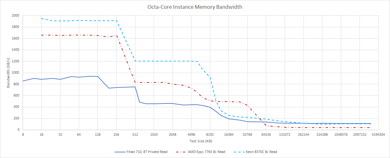
Shared cache bandwidth becomes more interesting as more cores are loaded. Yitian 710’s L3 can provide 141 GB/s of read bandwidth to eight cores. I don’t have data from Sapphire Rapids, but Intel’s Ice Lake roughly matches that performance. AMD can deliver a massive 530 GB/s to eight threads on Zen 3. Intel and AMD’s CPUs support 2-way SMT. Curiously, Intel gains significant bandwidth if all SMT threads are loaded, while AMD doesn’t see a lot of change.
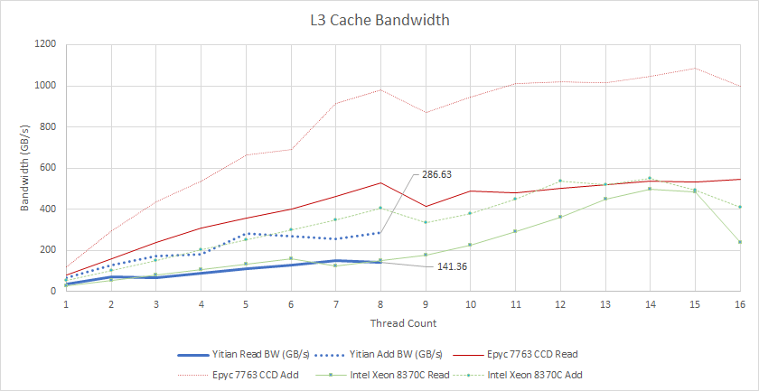
We can get more bandwidth with a read-modify-write pattern, because writebacks can often expose more parallelism. This method gives us 286 GB/s from eight Yitian 710 cores. Intel’s Ice Lake sees even more benefit, reaching 403 GB/s, while AMD gets a staggering 981 GB/s thanks to a very well optimized victim cache implementation.
While L3 caches handle traffic from multiple cores and provide many megabytes of capacity, core-private L1 and L2 caches serve a very significant portion of memory accesses. Compared to Neoverse N1, N2 adds another port to the L1 data cache, letting it serve three 128-bit loads per cycle. For a mobile core, this is a lot of load bandwidth, and eight Neoverse N2 cores can pull just short of 1 TB/s from their L1 caches. While that’s a good performance in isolation, Intel is a clear champion in core-private cache bandwidth thanks to a heavy focus on vector performance. This advantage extends to L2. In fact, Ice Lake enjoys more L2 bandwidth than N2 does from any cache level.
AMD takes a middle-of-the-road approach. Cores since Zen 2 offer enough L1D bandwidth to service two 256-bit loads per cycle, but lack Intel’s 512-bit datapaths. With matched eight-core instances, Epyc 7763 can’t offer as much core-private bandwidth as Ice Lake, but still outmatches Neoverse N2 by a large margin at all cache levels.
DRAM shows a different picture, though we’re limited by what we can see from an octa-core instance. Alibaba’s Yitian 710 has a DDR5 setup, compared to the DDR4 setup found on last-generation x86 chips, and achieves 111.95 GB/s with a 4 GB test size. Ice Lake falls just short at 103.69 GB/s. The Zen 3 VM is held back by its Infinity Fabric link, and only gets 40.23 GB/s. AMD’s two level interconnect setup might allow for exceptional L3 bandwidth and a cost-saving chiplet design, but can be limiting for DRAM bandwidth hungry workloads that aren’t very parallelizable.
Instruction Side Bandwidth
Cache setup affects the instruction side too. Compared to A710, ARM’s fixed 64 KB L1 instruction cache size provides slightly increased throughput for code footprints exceeding 32 KB. This advantage is somewhat limited as N2 can sustain well over 3 IPC when running code from L2. N2’s larger L2 cache can give it a significant frontend bandwidth advantage for bigger code footprints, especially if code spills out of A710’s smaller L2. However, A710 achieves better frontend bandwidth from L3 thanks to lower latency.
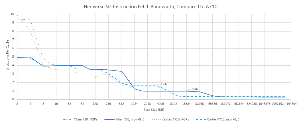
ARM often compares Neoverse N2 to N1, because they didn’t release any N-series server cores in between those two generations. For small code footprints, N2 can sustain 5 IPC by using its micro-op cache, though it’ll be interesting to see how often the core’s relatively small backend can keep up with such high frontend throughput. For larger code footprints, N2 enjoys far better L2 code fetch bandwidth, probably because N2 can track enough L1i misses to almost hide L2 latency. Both CPUs suffer very poor instruction bandwidth when running code from L3.

AMD and Intel’s competing CPUs generally enjoy higher frontend bandwidth, though analyzing x86 is a little more complex because of variable instruction lengths. We’re using 4 byte NOPs here, which is representative of average instruction lengths in integer code.
For small code footprints, AMD and Intel have a small lead because their cores are 6-wide. Neoverse N1 enjoys a small lead over Intel when running code from L2, but loses to AMD’s Zen 3, which has no problems sustaining 16 bytes per cycle from L2. Finally, AMD is a clear winner if code spills into L3.
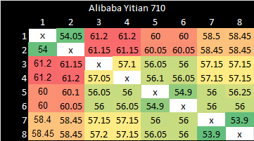
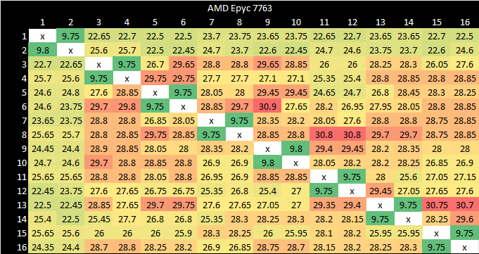
Core to Core Latency
Interconnects have to make sure all cores have a coherent view of memory even though they have separate private caches. Here, we’re seeing how long it takes for the interconnect to make a write from one core visible to another by using atomic compare and exchange operations. Within the octa-core instance, we see middle-of-the-road latencies at 50-60 ns. Adjacent cores see very similar latencies, so two cores may be sharing a mesh stop. Ampere Altra notably puts pairs of Neoverse N1 cores on the same mesh stop too. ARM’s CMN-700 can scale up to a 12×12 mesh, making core pairing unnecessary, but Alibaba may have chosen to do so anyway to keep mesh size down.
AMD has much faster ring interconnect within each core cluster. Latencies are higher if we have to go between clusters, but that won’t happen on an octa-core VM. If it does happen, transfers within a socket see about 100 ns of latency, or about 110 ns if the two cores are on different sides of the socket.
Intel’s Ice Lake uses a mesh, and achieves similar performance to Alibaba’s Yitian 710. Their newer Sapphire Rapids shows broadly similar behavior, though intra-socket latency goes up to the 70 ns range.
Accesses that require transfers between cores are about an order of magnitude rarer than L3 misses. But they do happen, and could affect performance if latency is particularly bad. Core to core latency on all of these CPUs is better than memory latency, so that sholdn’t be an issue here.
Final Words
The past few decades have seen the server market dominated by cores derived from client designs. Gradually, server cores distinguished themselves from their client versions with different cache setups and interconnects designed for better scalability. For example, Intel’s Xeons of 2008 used the same dies as client Core 2 CPUs. The 2010s saw Xeons use the same core architecture as client designs, but with larger ring buses to deliver more L3 cache and higher core counts. Later in the decade, Skylake widened the gap between client and server by using different L2 sizes and vector execution setups. AMD follows a similar strategy as Intel did in the early 2010s, using identical core designs but a different Infinity Fabric configuration to support higher core counts.
ARM is doing the same with Neoverse. N1 and N2 are both derived from Cortex designs, while a mesh interconnect and bigger caches allow higher core counts. ARM’s CMN-700 mesh makes Intel the closest comparison. Meshes from both companies provide consistently mediocre latency when bouncing cachelines between cores. L3 latency and bandwidth are poor, and high L2 hitrates are vital to keeping traffic off the slow mesh. This approach contrasts with AMD’s, which reuses desktop chiplets to provide very high L3 performance, but suffers more when dealing with L3 misses.

With respect to the cores, ARM is opening the throttle on mobile cores to make them meet server performance requirements. AMD and Intel in contrast are throttling back desktop cores to achieve higher density and better efficiency. Seeing ARM and x86 approach the same problem from different directions is quite fascinating. The result is that Neoverse cores are individually less capable than their x86 competition. Like its predecessor, Neoverse N2 should put in the best performance with integer code, but fall further behind with vectorized applications. But coming from a mobile background gives ARM better density to start with, so higher core counts may make up the difference.

Compared to Neoverse N1, N2’s core is a significant step up. Cortex A710 comes several generations after the Cortex A76, and N2 gets all of its advantages. A beefier out-of-order execution engine and more ability to extract memory level parallelism makes N2 a compelling upgrade over N1. I think ARM’s progress is acceptable, since they consciously exchange per-core performance for more cores.
However, I wish ARM made more aggressive changes. N2 comes two generations after N1 and enjoys a new process node. TLBs are an example. From 2019 to 2023, AMD’s L2 TLB went from 2048 entries on Zen 2 to 3072 entries on Zen 4, even though Zen 4’s TLBs have to work with larger 52-bit physical addresses. L2 capacity is another example. Intel’s Sapphire Rapids increases L2 capacity to 2 MB, up from 1 MB in Skylake and 1.25 MB in Ice Lake. Increased L2 hitrates help cope with poor L3 performance, a shortcoming shared by both ARM and Intel server interconnects. But three years after N1, ARM continues to use a 1 MB, 13-14 cycle L2 cache, running at very similar clock speeds. Finally, memory latency was roughly on par with x86 server chips in Ampere Altra and Graviton 2, but Yitian 710 regresses.
This might sound like nitpicking, but the server market is tough, as Intel and AMD both found out in their years of competition against each other. AMD’s K8 and K10 Opteron had a strong position in the server market until Intel rolled out Nehalem and Sandy Bridge based Xeons. Then, Intel had a dominant position until Rome, Milan, and Genoa presented increasingly stiff competition. Neoverse N1 may have gained a significant foothold, but ARM will have to fight tooth and nail to keep it. That means pulling all the stops to keep pace with your competitors. Making merely acceptable progress is risky.
ARM is somewhat sidestepping the strengths of AMD and Intel’s architectures by focusing on the high density sector. But while ARM sort of won by default in 2019 because no one was focusing on maximizing density, the situation in 2023 is different. Ampere is rolling out server chips with up to 192 cores, based on their in-house Siryn architecture. AMD’s Bergamo will field 128 cores, matching Yitian 710 and potentially bringing more per-core performance. Finally, Intel’s Sierra Forest is rumored to pack 144 efficiency oriented cores and could launch within a few dozen Pluto years.
So, ARM has an interesting fight ahead of them. Personally, I think they have a good chance of rising to the challenge. Like the Cortex A710, Neoverse N2 by itself is a very solid design, with a lot of changes made in the right places. ARM has also executed well in the past, even when making drastically different designs instead of making changes on top of a solid base. A future Neoverse N3 will be interesting to see, and I hope it comes sooner than later with some well executed improvements.
If you like our articles and journalism, and you want to support us in our endeavors, then consider heading over to our Patreon or our PayPal if you want to toss a few bucks our way. If you would like to talk with the Chips and Cheese staff and the people behind the scenes, then consider joining our Discord.
N2's L1 I-Cache should be 64KB in your pipeline diagram.