
ARM’s Cortex A710: Winning by Default

ARM Ltd has been dominating the Android world for the better part of the last decade, with their 7-series cores at the forefront of their success. Throughout the late 2010s, the Cortex A73, A75, and A76 steadily iterated on performance while maintaining excellent energy efficiency. Qualcomm, and then Samsung decided licensing ARM’s cores would be easier than trying to outdo them. Apple remained a notable rival, but their core designs were not available outside a closed-off ecosystem. By the time Cortex A78 came around, ARM had no real competition.
ARM’s Cortex A710 continues that dominance. It takes A78’s successful formula and tweaks it to improve performance and efficiency. Efficiency is especially prioritized, with the core seeing cuts in some areas as ARM tries to get more done with less power. A710 claims to provide a 30% uplift in power efficiency or a 10% performance increase within a fixed power envelope when compared to a A78 core with half as much L3 cache. Alongside these improvements, A710 gains Armv9-A and SVE support.
System Level
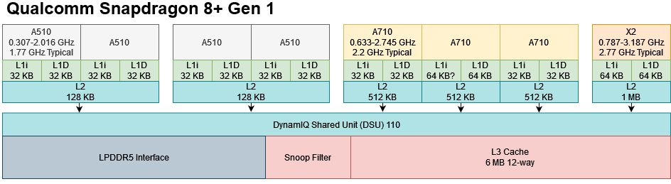
I’m testing the A710 with Qualcomm’s Snapdragon 8+ Gen 1, in the Asus Zenfone 9. This SoC has three A710 cores, alongside four A510 cores and a single X2 core. Qualcomm likely connects all of these cores with ARM’s DynamIQ Shared Unit (DSU) 110. The DSU-110 provides an interconnect that lets ARM licensees implement up to 12 cores, and link them to memory and peripherals. Optionally, the DSU-110 can support a L3 cache with up to 16 MB of capacity. For the Snapdragon 8+ Gen 1, Qualcomm has chosen 6 MB of L3 cache. ARM conducted their performance and power estimates with 8 MB of L3, so Qualcomm is opting to reduce area usage for a small performance hit.
To ensure coherency, the DSU-110 maintains snoop filters. Like the L3, the snoop filter is separated into slices linked in a dual-ring setup, with addresses striped across the slices. The DSU-110 thus acts a lot like Sandy Bridge’s ring bus, and allows bandwidth to scale with slice count. If we bounce cache lines between cores with a “core to core” latency test, the Snapdragon 8+ Gen 1 behaves a bit like any recent Intel or AMD system. Latencies vary depending on which slice the cacheline is homed to.
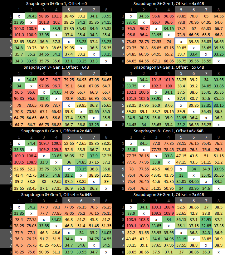
Additionally, cores can be placed into a dual core clusters. Shared cluster logic allows better area efficiency, but with reduced performance. Qualcomm has opted to do this for the A510 cores. A710 cores are not placed into clusters, and generally enjoy good latency when bouncing cachelines to other cores.

Like Haswell, the DSU-110 places cores and the ring bus on separate clock domains to improve energy efficiency, at a slight L3 latency cost. Each core or core cluster is placed on a separate clock and power domain. The Snapdragon 8+ Gen 1’s A710 cores can clock anywhere from 633 MHz to 2.745 GHz, although hitting the maximum boost clock is rare in practice. When loaded, the A710 cores boost to 2.22 GHz after a short 20 ms delay, and then tend to sustain that clock speed indefinitely.

Because the phone is running Android, some aspects of the core (like huge pages and SVE) will be impossible to test. Test results will be noisy too, especially when compared against results from a desktop operating system.
Core Overview
The Cortex A710 is a 5-wide out-of-order core with a 10 stage pipeline. Its out of order execution engine combines decent reordering capacity with a large distributed scheduler setup and ample execution resources. It looks a bit like a desktop core from a couple generations ago, but targets far lower clock speeds to maximize power efficiency. As with other ARM cores, many aspects of the core can be customized in order to hit the power and performance targets desired by an implementer.
Here’s an approximate block diagram of the core, as implemented in the Snapdragon 8+ Gen 1. Undocumented structure sizes are estimated through microbenchmarking, so expect a fair degree of inaccuracy.
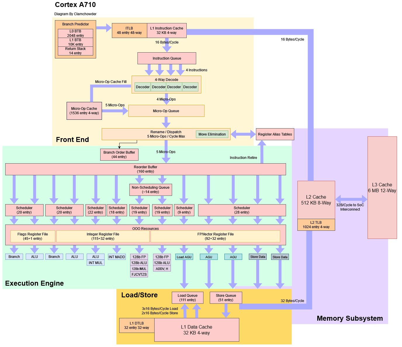
Qualcomm’s Snapdragon 8+ Gen 1 sets up its A710 cores with 32 KB L1 and 512 KB L2 caches. Strangely, the second A710 core appears to have a 64 KB L1 data cache, and possibly a 64 KB L1 instruction cache as well. ARM allows different cores of the same type to be configured with different cache capacities on the same SoC. Qualcomm may be trying for different levels of performance even within its A710 cores.
Frontend: Branch Prediction
A CPU’s branch predictor is responsible for telling the frontend where to fetch the next instructions from, without waiting for previously fetched branches to finish executing. A fast and accurate branch predictor will help keep the core fed while improving energy efficiency. Therefore, ARM did not skimp on the branch predictor. Pattern recognition capabilities are comparable to those of desktop CPUs from a few generations ago.

It’s not a match for Zen 3 or Zen 4’s giant branch predictor, but ARM needs to be careful because the branch predictor itself can consume significant core area and power. Past a certain point, a bigger branch predictor will give diminishing returns.
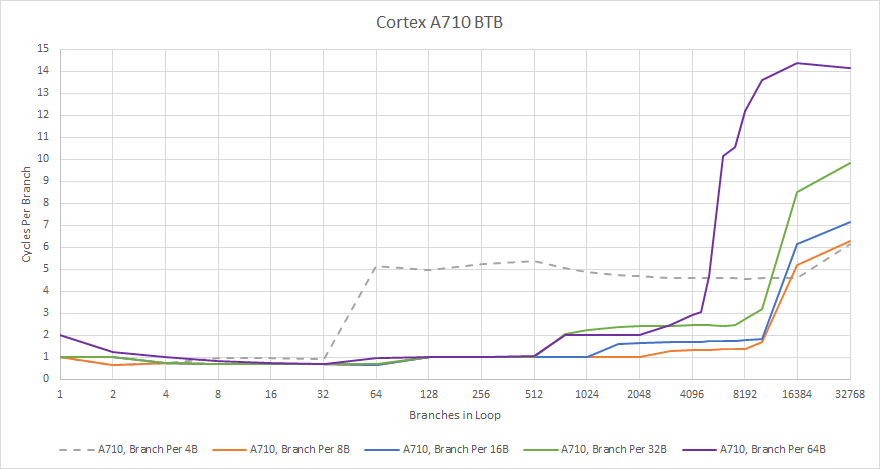
Branch predictor speed is important too. Taken branches tend to show up once every 10-20 instructions. A branch predictor that stalls the fetch unit for too long after a taken branch can potentially cause frontend bandwidth bottlenecks. ARM has not skimped here at all. A710 has a large 2048 entry first level BTB that can handle back-to-back branches. Effective capacity for this fast BTB level is probably around 512 to 1024 branches though. That 2048 branch figure was achieved with a branch every 8 bytes, and having a branch every two instructions is a touch unreasonable.
A710 has a 10K entry second level BTB. This gives the core a substantial amount of branch target caching capacity, and is still quite fast. Depending on branch distance, this main BTB can deliver targets with a 1-3 cycle penalty.

Multi-target branches require more sophisticated prediction, because the branch predictor has to pick between multiple targets. A710 has a very capable indirect branch predictor. It can handle up to 64 different targets for a single branch before seeing substantial penalties. With a modest eight targets per branch, A710’s indirect predictor can track an incredible 4K targets. A710 might be using the large main BTB to store indirect targets, instead of using a dedicated indirect target array.

Returns are a special case of indirect branches, because they typically go back to a corresponding call site. A710 predicts returns with a 14 entry return address stack, but maintains good performance with very deep nested calls. The core is probably falling back on its indirect predictor if the return stack overflows, similar to Skylake.
Frontend: Fetch and Decode
After receiving a fetch address from the branch predictor, the frontend has to bring the specified instructions into the core as fast as possible. The A710 has a 32 KB, 4-way set associative L1 instruction cache. It’s virtually addressed and physically tagged, so the frontend indexes into the L1 instruction cache in parallel with looking up the virtual address in the 48-entry fully associative iTLB. Assuming a L1i hit, the frontend passes the instruction bytes to a four-wide decoder, which translates instructions into the core’s internal micro-op format.

Micro-ops are passed on to the renamer, and also filled into a 1536 entry, 4-way micro-op cache. Small code footprints can run from the op cache, which can deliver 5 micro-ops per cycle. As with all op caches, bandwidth benefits can be even higher when pairs of instructions are fused into a single micro-op, because fusion takes place before micro-ops are filled into the cache. This is particularly visible when testing instruction bandwidth with NOPs, since A710 can fuse pairs of NOPs into a single micro-op.
A710 actually has less frontend bandwidth than A77 and A78. Op caches on both of those prior architectures could deliver 6 micro-ops per cycle, giving them impressive bandwidth for a mobile core. But increasing core width past a certain point provides minuscule performance gains. A710 aims for better power efficiency even on the same process node, so there’s no room for flashy features that don’t pull their weight.
Intel’s op caches are an interesting comparison. Both companies used a 1536 entry op cache for three major generations. ARM did so with the A77, A78, and A710, while Sandy Bridge, Haswell, and Skylake did the same on Intel’s side. ARM and Intel claim 85% and 80% hitrates for A77 and Sandy Bridge’s op caches, respectively. I call bullshit on both figures. AMD’s op cache has similar goals, but is physically tagged (but virtually micro-tagged) and therefore can be competitively shared between two SMT threads. In contrast, ARM and Intel’s op caches are virtually addressed. Intel’s cache can be flushed by TLB maintenance operations, and the same probably applies to ARM’s.
We can test instruction bandwidth by filling an array with instructions, jumping to it, and seeing how long it takes for the frontend to get through it. For small code footprints, A710’s micro-op cache can deliver a notable bandwidth increase, especially in corner cases involving instruction fusion. Past that, the core maintains high instruction throughput thanks to the four-wide decoder.
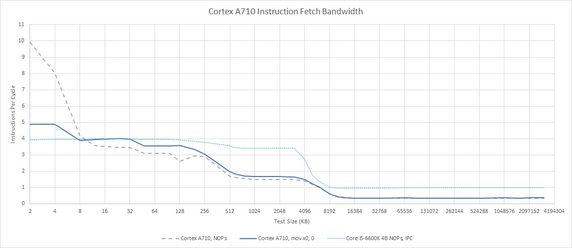
For larger instruction footprints, A710 can run code from L2 with almost no penalty, subject of course to branch prediction limitations. It’s a massive step up from older ARM cores like the Neoverse N1, and places the A710 on the same level as Skylake and Zen 1. Instruction throughput doesn’t take a sharp hit until after code spills out of L2, but A710 maintains passable IPC even in that case. At that point, Skylake tends to do better.
Renamer and Allocate
Micro-ops from the frontend are fed to the renamer, which maps architectural registers into the backend’s physical register file. Every instruction that writes to a register gets assigned a new physical register. Instructions therefore don’t get delayed in the backend scheduler for anything other than a true read-after-write dependency. Besides registers, the renamer allocates other backend resources as necessary. For example, all instructions need a reorder buffer entry. Stores and loads need a queue entry in the load/store unit, and so on.
Besides resource allocation, the renamer can implement optimizations that expose more parallelism to the backend, or even complete certain instructions without requiring an execution pipe. For example, instructions that copy data between registers can be handled by manipulating the architectural to physical register mappings. A710 can eliminate register to register moves, but can fail to do so if presented with chained, dependent moves. AMD and Intel’s recent CPUs can do that, but ARM’s capability should be adequate for a large percentage of cases.
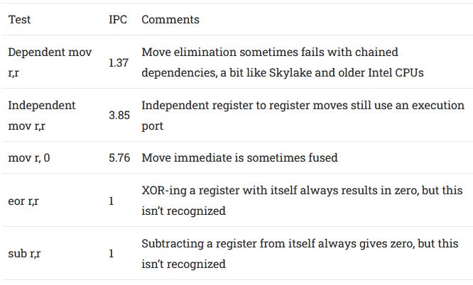
On x86, compilers or programmers often zero registers with math operations that will always result in zero, taking advantage of shorter instruction lengths on x86 when you don’t have to encode an immediate value. ARM on the other hand uses fixed instruction lengths, so there’s no advantage to XOR-ing a register with itself over moving an immediate value of zero into it. A710 can’t recognize zeroing idioms, but it’s not a big deal.
In line with the frontend width reduction, A710 sees its renamer width cut from 6-wide to 5-wide. Again, A710 aims to improve efficiency first, and performance second. Cutting unused core width is a good way to do that, especially at the rename stage. On other cores, the renamer is often the narrowest part of the core, and I suspect that’s no accident. Multiple instructions can reference the same architectural register and go through the renamer in the same group. On the 6-wide A77, the register alias tables would need to handle at least 12 reads and 6 writes per cycle. To make things harder, the renamer may have to rename the same architectural register several times in the same cycle, and correctly assign newly allocated registers to dependent instructions in the same group. The renamer probably has some highly ported structures with tight timings, and making it smaller could save both power and area with little performance impact.
Out of Order Execution
Out of order execution involves executing instructions when their required inputs are ready, without respect to program order. Then, results are committed in program order to produce correct user-visible results. Deeper buffers allow the CPU to move farther ahead of a stalled instruction in hopes of keeping the execution units busy. For a while, low power cores could only afford small execution engines. Reorder buffers rarely had more than 64 entries, and even when they were larger, scheduler and register file capacities presented serious limitations. Cortex A76 was a bit of an inflection point, with a 128 entry ROB and other structures sized well enough to back it up.

A710 continues the trend. Most structures are substantially larger than A76’s, letting A710 cope better with cache and memory latency. The FP register file notably didn’t see a capacity increase, but A710 has a trick up its sleeve. Pairs of scalar FP instructions can be fused, and only consume a single vector register. Scalar FP instructions are quite common even in software that takes advantage of vector instructions, A710’s fusion ability can make the FP register file go farther than its entry count would suggest.
Instruction Scheduling and Execution
Schedulers track instructions until their data dependencies are satisfied. A710 uses a mostly distributed scheduler setup, which requires careful tuning because the renamer will stall if it can’t get a free entry from a particular scheduler, even when other schedulers have free entries. ARM addresses this by making most of the schedulers quite large. A710’s integer cluster has more scheduling capacity than Zen 2’s, which uses a similarly distributed scheduler setup. This is an excellent improvement over older ARM cores, where small scheduling queues could be a serious limitation.

Skylake’s more unified scheduling setup is less likely to stall on an individual queue filling up, but ARM should compete quite well by virtue of having about 50% more scheduler capacity across its distributed queues. A710 absolutely has a desktop class scheduler, and one that’s arguably overbuilt considering its ROB and register file sizes.
A710’s integer cluster has four pipes, and documentation suggests all four can handle most common integer operations while three pipes can handle instructions that deal with flags. However, I could not sustain four adds, or integer logic operations per cycle, regardless of whether they access flags. Mixing in multiply-add instructions does let me achieve more than 3 instructions per cycle, suggesting that the fourth pipe is dedicated to multi-cycle operations. If integer addition throughput is a bottleneck, a program could theoretically complete four such operations per cycle by mixing in MADD instructions with a multiplier of 1. In any case, three ALUs should not present a bottleneck for most code sequences.

For vector and floating point operations, A710 only has two pipes. Even though scalar FP instructions can be tracked as a fused micro-op, it’s un-fused at the execution stage and throughput is limited to two operations per cycle. However, both pipes can handle common floating point operations, and do so with low latency. Packed 128-bit operations execute with the same throughput and latency as scalar ones, as is typical for most CPUs.
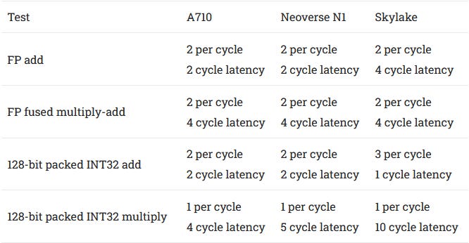
Desktop and server cores use significant die area to deliver 256-bit or 512-bit vector execution. As a mobile core, A710 can’t afford this. Still, it should do a passable job when confronted with the occasional vector code sequence.
Address Translation
After the AGUs have generated virtual addresses, they’re translated into physical addresses. A710 has a two level TLB setup for caching address translations. ARM has opted to use a rather small first level DTLB, probably to achieve better energy efficiency. Three memory accesses could require 3 * 32 = 96 DTLB tag checks, and the A710 would have to be capable of doing that every cycle. Prior ARM CPUs have used larger first level TLBs. For example, the A73 has a 48 entry micro-TLB. However, increased load/store throughput likely made that design too power hungry. Interestingly, the A73 would have to do a maximum of 48 * 2 = 96 DTLB tag checks per cycle, matching the A710 in that regard. Desktop cores tend to use larger first level TLBs. Skylake has a 64 entry L1 DTLB, while Zen 4 has a 72 entry one. But that’s not a hard and fast rule. Bulldozer uses a 32 entry DTLB, much like A710.

On a DTLB miss, A710 can load an address translation from the 1024 entry L2 TLB, with a 5 cycle latency penalty. Capacity-wise, A710’s L2 TLB is comparable to Haswell’s, but again it falls behind what we see from recent desktop cores. Skylake has a 1536 entry L2 TLB, while Zen 4 has a hefty 3072 entry one. Despite massive process node improvements over the past few years, ARM has decided not to implement a larger L2 TLB. The Cortex A73 from long ago also has a 1024 entry, 4-way L2 TLB.
A710 also keeps address sizes down in order to improve power consumption. Desktop cores often serve double duty in servers, and therefore use 48-bit or even 52-bit physical addresses to allow massive pools of memory. 40-bit physical addressing limits A710 to 1 TB of memory. Servers sometimes have multiple terabytes of DRAM, and need even more address space to handle peripherals. Cell phones don’t need as much DRAM, yet.
Store Forwarding
In-flight memory accesses have to be checked against each other to make it look like they executed in order. Writes have to be immediately visible to a read that happens after. Loads therefore might have to get their data from a prior in-flight store, since data from the cache hierarchy would be stale. CPUs have a fast forwarding path designed to handle the easiest and most common cases, and fall back to a slower path to ensure correctness if they meet something the fast path can’t handle. Often, that slow path involves waiting for the store to retire, then loading the data from cache.
A710’s fast forwarding path can only send the top or bottom half of a store to a dependent load. Other overlap cases incur a 10+ cycle penalty, even when the load is completely contained within the store.
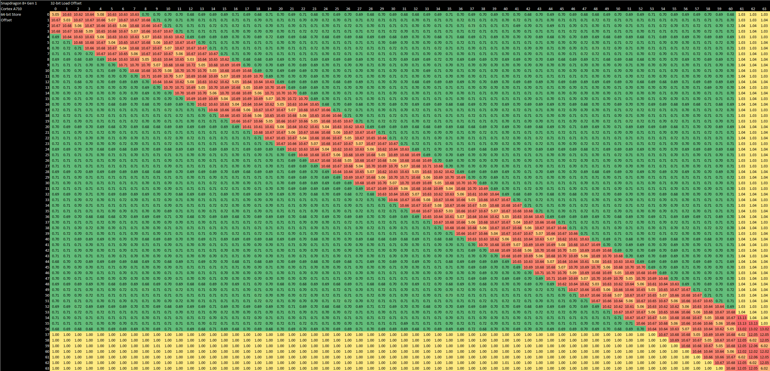
AMD and Intel have more advanced fast forwarding mechanisms, which always work as long as the store completely contains a dependent load. However, they take more cycles for partial overlap cases, as they have longer pipelines designed for higher clock speeds.
Cache and Memory Access
ARM’s cores see massive variance in their cache setups depending on how they’re implemented. To summarize the configuration options:

In the Snapdragon 8 Gen 1, Qualcomm has given the A710 a triple level cache hierarchy. They’ve selected the larger L2 size, but were pretty conservative with the other options. 32 KB L1 caches are quite common, and a 6 MB L3 cache should be decent for most applications.
Older cores like the Cortex A75 offer surprisingly competitive L1D latency. Mobile CPUs have stayed around the low 2 GHz range, and the Snapdragon 8 Gen 1’s A710 cores are no exception. The A75 clocks slightly lower, but compensates with 3 cycle access to its L1D. A710 takes four cycles, putting it in company of higher clocked desktop cores, just without the clocks.

Accesses that miss the L1 can pull data from the 512 KB L2 cache. The L2 is inclusive of L1D contents, and can be accessed with a latency of 13-14 cycles. A75 had 12 cycle L2 latency, but clock speeds give A710 a clear edge. If accesses miss the L2, they go across over a CPU bridge to the DSU-110 interconnect. From there, they can be serviced by an optional L3 cache, or DRAM.
The DSU-110’s L3 cache acts like AMD Zen’s. It’s a victim cache that’s inclusive of L2 contents for shared data, but exclusive for core-private data. On the Snapdragon 8 Gen 1, we get a 6 MB L3 with around 20-21 ns of latency, or a bit north of 50 cycles. L3 latency is similar to the Snapdragon 670’s, but capacity makes all the difference here. 1 MB of last level cache is embarrassingly inadequate. 6 MB of L3 isn’t great, but it’s a match for older, midrange desktop chips like the i5-6600K, and enough to offer passable hitrates across a range of applications.
Memory latency is typically terrible on mobile chips, thanks to LPDDR. A710 can’t escape this, but fares better than A75. Address translation penalties likely contribute to A710’s advantage, because paging structures are more likely to be held in A710’s larger caches. However, desktop CPUs like Skylake with similar L3 cache capacity deliver much, much better latency, even when page walks are in play.
Bandwidth
A710’s triple-port data cache gives it a bandwidth advantage compared to older mobile cores. With 128-bit vectors, A710 can pull 48 bytes per cycle from its L1 data cache. However, it’s still no match for a desktop core designed to support 256-bit vectors.

L1 misses result in a L2 lookup. A710’s L2 can feed the core with about 20 bytes per cycle of sustained bandwidth. That’s a large improvement over older ARM cores, but can’t match the 32 bytes per cycle that most desktop chips can get from their L2 caches. On a L2 miss, requests are placed into a transaction queue (TQ). The TQ can have 48, 56, or 62 entries depending on the implementer’s mood. TQ capacity is split between write, read, and snoop transactions, with watermarks set to avoid starving requests of a particular type.
ARM’s large transaction queue enables decent L3 performance from a single core, at just below 16 bytes per cycle. On a per cycle basis, A710 has similar L3 bandwidth to Skylake. However, Skylake still enjoys a significant L3 bandwidth advantage from clocking much higher.
Memory bandwidth from a single core is also very good. Despite higher memory latency, a single A710 core can pull about the same bandwidth from memory, again thanks to the large L2 transaction queue. LPDDR latency can be overcome with an adequate amount of cope, and A710 does exactly that.
Final Words
ARM has a firm grip on the Android market. Samsung, Qualcomm, and MediaTek may develop their own SoCs, but all use CPU core designs from ARM (the company). ARM’s situation today therefore mirrors Intel’s heading into 2015. Just as Intel’s Skylake competed with prior Intel designs, ARM’s A710 is basically competing with the company’s own last generation cores. The market is ARM’s to lose, and they’ll win by not screwing up.
Therefore, A710 is a conservative design, and even more so than Skylake. ARM does not describe their cores particularly well, but documented structure sizes often don’t change (or even regress) compared to A77. Such moves are consistent with ARM’s goals of prioritizing efficiency over absolute performance. It’s also the correct business strategy for ARM. The best way to win a chess game when you know your opponent won’t show up is to not pull an all-nighter studying your nonexistent opponent’s favorite openings, only to oversleep and miss the match.
ARM does exactly that. Similarities to A77 and A78 mean ARM can inform A710’s design with years of real world data. Keeping a small change count means there are fewer moving variables when estimating power efficiency and performance. It’s a boring strategy, but that’s what prudent business decisions sometimes are.
That’s not to say A710 is a bad core, because it’s a competent low power design. It’s a huge step up from (much) older cores like the Cortex A75. Higher core throughput, excellent frontend bandwidth when running code from L2, and better instruction latencies make it a compelling upgrade. Instruction fusion helps increase effective width and reordering capacity, while its large scheduler helps make the most of its ROB and register files. But increasing transistor budgets should let ARM do more. Compared to older desktop cores, A710 has competitive throughput but will likely struggle with larger data footprints thanks to its small TLBs. Its memory disambiguation mechanism isn’t as robust. Renamer optimizations are still a decade behind the state of the art. Cache latency remains high. A710 is a solid offering and good enough to compete with ARM’s previous cores, but there is room for improvement. Given a choice between the A710 and an A77 or A78, a customer would probably pick the A710, and that’s all ARM needs.
I wonder what would have happened if Qualcomm and Samsung remained viable competitors. As a kid, I remember watching AMD’s K8 push Intel to create giants like Conroe, Nehalem, and Sandy Bridge. A Sandy Bridge moment for ARM would be exciting to see today, and ARM is definitely capable of making big strides. They redid their entire core design going from A75 to A76/N1, and delivered a solid result without tripping over themselves. Thankfully, motivation may be coming soon. Rumors suggest Qualcomm plans to launch a new in-house core before the heat death of the universe. In the server world, Ampere is working on their in-house Siryn core. Siryn-based server CPUs could be widely available in time for our grandchildren’s grandchildren to contemplate pre-ordering one for their grandchildren. With that in mind, I hope to see ARM picking up the pace in upcoming designs.
If you like our articles and journalism, and you want to support us in our endeavors, then consider heading over to our Patreon or our PayPal if you want to toss a few bucks our way. If you would like to talk with the Chips and Cheese staff and the people behind the scenes, then consider joining our Discord.