
Correction for A710/Neoverse N2’s FP Scheduler Layout

As recent events have made clear, testing is hard. Determining a CPU’s scheduler layout involves a lot of testing, making mistakes likely. I made one such mistake for Cortex A710, which led to a block diagram with incorrect scheduler capacities for the floating point pipes.
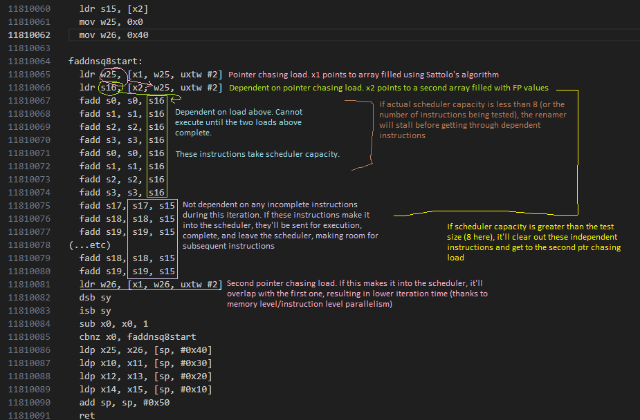
To understand what happened, let’s first go over how we can determine CPU structure sizes. I’m using Henry Wong’s methodology, which involves putting a pile of filler instructions between two cache misses. His PHD thesis is also a good read, and I highly recommend going over that. Henry focused on measuring reorder buffer and register file capacities, but the same methodology can be applied to other core components. For schedulers, that involves making the filler instructions dependent on the pointer chasing load results. If the filler instructions exhaust a backend resource, it’ll cause a stall at the renamer and prevent the two cache misses from overlapping. That shows up in the test as a far higher iteration time.
That’s all well and good, but measuring scheduler sizes adds another level of difficulty because the scheduler layout is variable. To use Henry Wong’s words:
First, one must decide whether to build a unified scheduler where all execution units share the same pool of waiting instructions, or a distributed scheduler where each execution unit has its own private scheduler. A distributed scheduler then requires choosing a scheduler size for the scheduler attached to each execution unit. In some microarchitectures, there can even be schedulers where certain execution units (e.g., two integer ALUs) are unified while the rest are distributed.
Henry Wong, A Superscalar Out-of-Order x86 Soft Processor for FPGA
Intel has used a unified scheduler setup in their P6 line, while AMD and ARM have trended towards more distributed layouts. A unified scheduler’s size is easier to measure, because I can use an instruction that goes to any of its ports. With a distributed scheduler, I need to test the size of each queue. When the scheduler layout is completely unknown, I also have to determine the scheduler’s layout to begin with. That involves mixing instructions that go to different ports. If the instruction mix sees increased scheduling capacity, then each port has a different scheduling queue. If not, they’re both behind a unified scheduler.
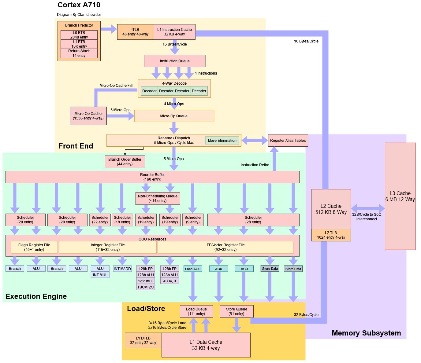
For the Cortex A710, ARM has (un)helpfully published the following:

None of the scheduler (issue) queue sizes are published, so I’m starting from ground zero. For the FP/ASIMD pipes, I tested FP adds and SVCTF (signed fixed-point convert to floating point). FP add testing was accomplished by loading a value from a separate array, using the result of the preceding pointer chasing load as an index. Testing SVCTF was more straightforward, as I could simply use it to convert the pointer chasing load’s result to a floating point value.
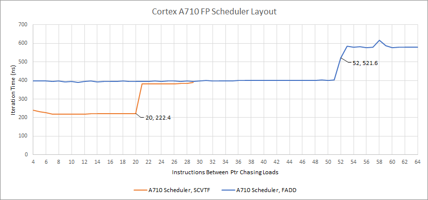
The problem here is that I simply hit ctrl+f in the optimization guide to figure out which port SCVTF went to. However, SCVTF appears several times in there, and goes to different ports depending on which form is used.
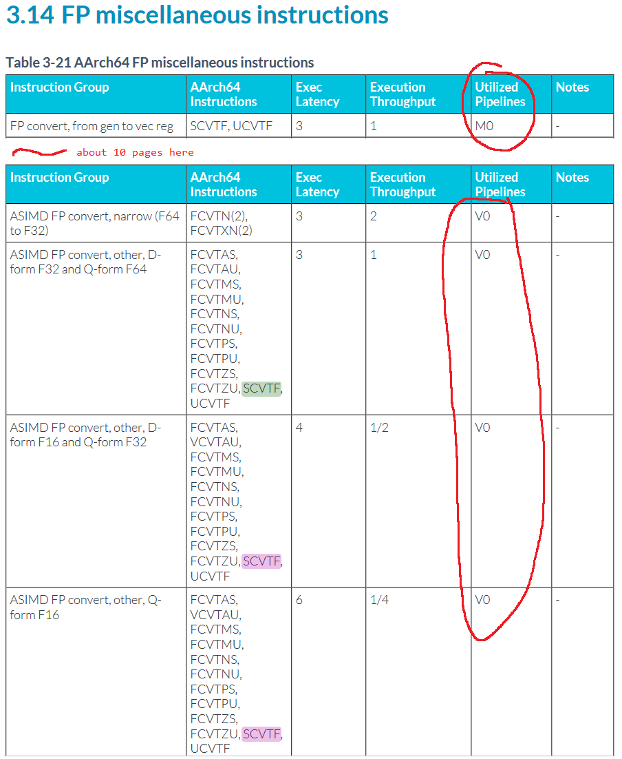
I used the form that takes a general purpose integer register and converts it to a FP result. Unfortunately, that form uses M0, a multi-cycle integer pipe. I wound up measuring scheduler capacity for that pipe instead of V0, but didn’t realize it. Using a different form that used two ASIMD/FP registers as inputs would have fixed the problem. But I found the problem while testing Cortex X2.
While testing Cortex X2, I added a test for FJCVTZS (FP Javascript convert to signed fixed point, rounding towards zero), because it’s one of the only single-pipe operations on that core. FJCVTZS would only go down pipe V0, making it ideal for seeing whether V0 had its own scheduling queue. I re-ran the test on A710, and was surprised to see different results. Double checking the manual indicated I had been testing the wrong port.

I also added a test for ADDV, which does a horizontal add across a vector, because it goes to port V1 on A710 and either V1 or V3 on Cortex X2. This is also a potential landmine because it has several forms. At first I used the variant that adds byte-sized elements, before realizing it actually decodes into two micro-ops – one that uses V1, and another that can use any vector pipe. That goes to show how easy these mistakes are to come by. Thankfully, the one that uses half-sized (16-bit) elements only decodes into a single micro-op that goes into V1.
Thus, the ADDV test above should show scheduling capacity available for the V1 pipe, while the FJCVTZS test shows scheduling capacity for the V0 pipe. When two pipes have exactly the same scheduling capacity, I also have to consider whether it’s a unified scheduler (i.e. the same queue feeds both ports). To do this, I can use either an instruction that can go down both pipes (FADD), or a mix of ADDV and FJCVTZS. The resulting increase in observable scheduler capacity indicates it’s a distributed scheduler with two 30 entry queues:
But That’s Not It
A 30-entry scheduler sounds pretty big, especially for a low power core. Generally, if something sounds too good to be true, it probably is. And we’ve seen how a naive scheduling capacity test could be screwed up too. AMD puts a large 64 entry non-scheduling queue in front of Zen’s FP scheduler. If we simply see how many incomplete operations the CPU can track before stalling the renamer, Zen will appear to track 96 even though its scheduler can only examine the first 36 and send them for execution.
To test for this, I have to think outside the box and apply Henry Wong’s methodology with a twist. Instead of seeing if a scheduler can handle N instructions by putting N instructions between pointer chasing loads, I place more instructions than I know it can handle, but not all of them are dependent. Independent instructions can exit the scheduler, making room for subsequent ones. By varying how many dependent instructions come before independent ones, I can figure out true scheduler size.
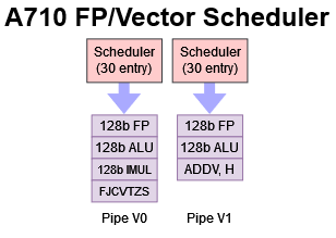
After writing tests for those, it’s clear that A710 is using non-scheduling queues. Specifically, the 30 incomplete instructions we could see the core track before can be divided into 19 in a scheduler, and 11 in a NSQ.

That gives another reason for why hitting both pipes together doesn’t provide double the scheduling capacity. The NSQ is likely shared, because we see double the scheduling capacity, but not double the NSQ capacity. In short, it probably looks like this:

Final Words
Creating block diagrams is hard, especially when there’s next to no information published about the core. The more things I have to measure instead of using documentation for, the higher the chance of error. That’s especially the case for me (personally) because I’m doing this with limited time. I have to balance what I do for Chips and Cheese with my full time job as a software developer, as well as my personal life and other interests.
But for now, it looks like no one else is investing the effort to document CPU details whenever they aren’t straight-up disclosed by the manufacturer. Hopefully my efforts will encourage ARM, Intel, and AMD to publish more details. Because if they don’t, I’ll publish it for them and probably make a mistake along the way.

Hopefully this will encourage other reviewers to do deeper dives into hardware. The macro-benchmarking scene benefits from a lot of reviewers testing the same thing. For example, Linus Tech Tips, Gamers Nexus, and Hardware Unboxed will all run a set of game tests on the same GPU. They can easily see if they need to double check a result if it looks like an anomaly compared to other results across the internet. I don’t have that luxury because it seems like no one else is testing the things I’m interested in, so mistakes are more likely to go unnoticed.
With that, I’d like to call on others in the tech scene to do deeper dives. This sort of testing is far more ideal for full time reviewers because of the time commitment. The skill floor isn’t the lowest, but it’s also not the worst. All you have to do is be familiar with C and assembly programming, and get a grasp of how CPU architectures are typically designed from the large amount of scientific literature out there. You don’t even have to come up with all the tests yourself, because you can read someone’s PHD thesis or other publication, and adapt their methodology to measure other things. Come on everyone…
I will revise the A710 article, and the N2 article where appropriate when I have time. The next week is looking to be a busy one, with concurrent projects at work, and Hot Chips coming up.
If you like our articles and journalism, and you want to support us in our endeavors, then consider heading over to our Patreon or our PayPal if you want to toss a few bucks our way. If you would like to talk with the Chips and Cheese staff and the people behind the scenes, then consider joining our Discord.