
AMD’s Radeon Instinct MI210: GCN Lives On

AMD, Nvidia, and Intel have all diverged their GPU architectures to separately optimize for compute and graphics. While Intel and Nvidia’s compute architectures tend to be close relatives of their contemporary graphics architectures, AMD has taken a different approach. Their GCN architecture, which dates back to late 2011, was already very capable for compute applications. GCN needed a lot of work in flight to shine and graphics workloads weren’t always like that, so RDNA took over for graphics. But GCN’s compute potential meant it survived and continued to evolve under a new name: CDNA. We’ve covered architectures from both lines, so take a look at our CDNA 2 and RDNA 2/3 articles for background info.
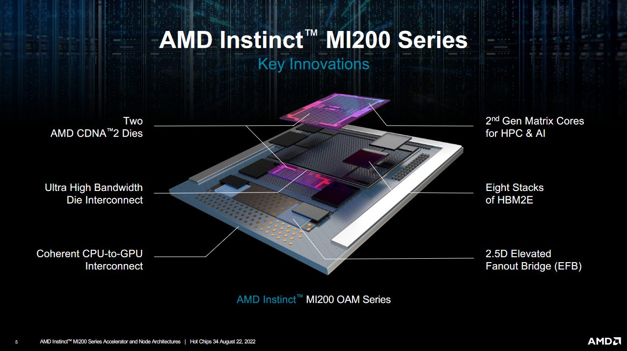
Here, we’re going to be looking at AMD’s Instinct MI210. It features a massive 724 mm2 die fabricated on TSMC’s 6 nm process. Just like the H100, AMD’s MI210 goes wide and slow with 104 compute units (CUs) running at up to 1.7 GHz. Like Nvidia’s compute GPUs, AMD uses HBM2e memory to provide tons of VRAM bandwidth. AMD gives a 300W total board power figure, putting it in the same ballpark as the Nvidia H100 PCIe’s 350W TDP.
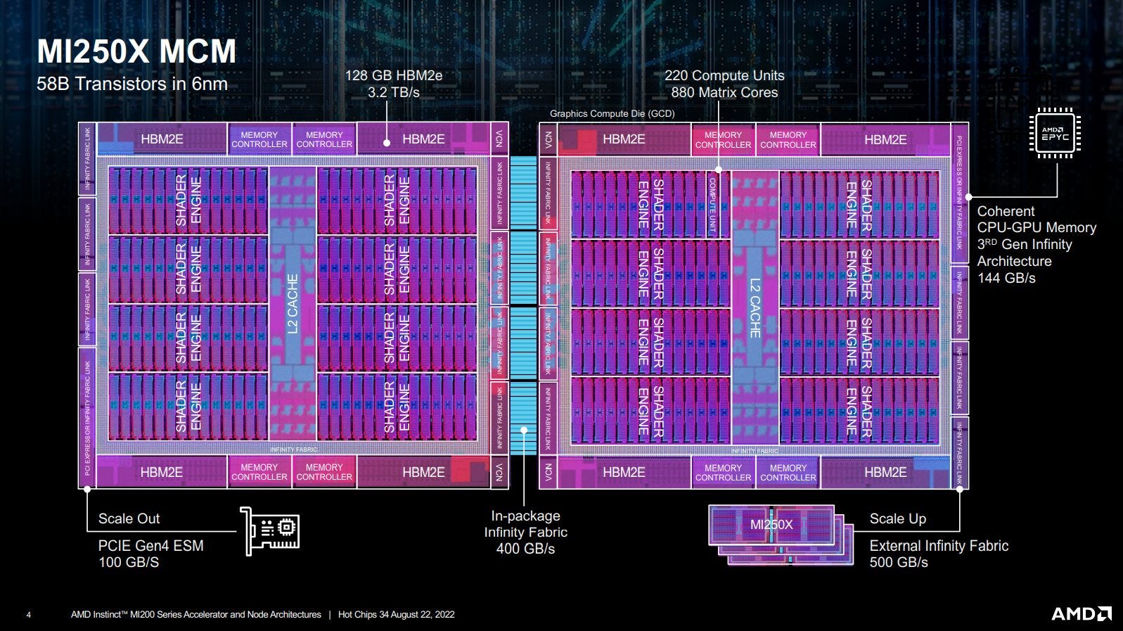
Nvidia’s H100 is an obvious competitor. However, the comparison isn’t perfect because H100 is a larger GPU. Nvidia’s H100 has a larger 814 mm2 die fabricated with on a “4N customized” node, which is a derivative of TSMC’s 5 nm node. MI210’s die won’t be cheap, but it should cost quite a bit less than H100’s. Dell appears to be selling the MI210 for just shy of $15,000, while Nvidia’s H100 PCIe card costs around twice as much. To fill out the top end, AMD combines two CDNA 2 dies in products like the MI250X.
Cache and Memory Access
CDNA 2 uses a simple two-level caching setup inherited from AMD’s GCN days. Each compute unit has 16 KB vector and scalar caches. Memory accesses will typically go down the bandwidth-optimized vector path. The scalar memory path is used to efficiently handle values that get used across a wavefront. Scalar values are often used for control flow, address generation, or constants.
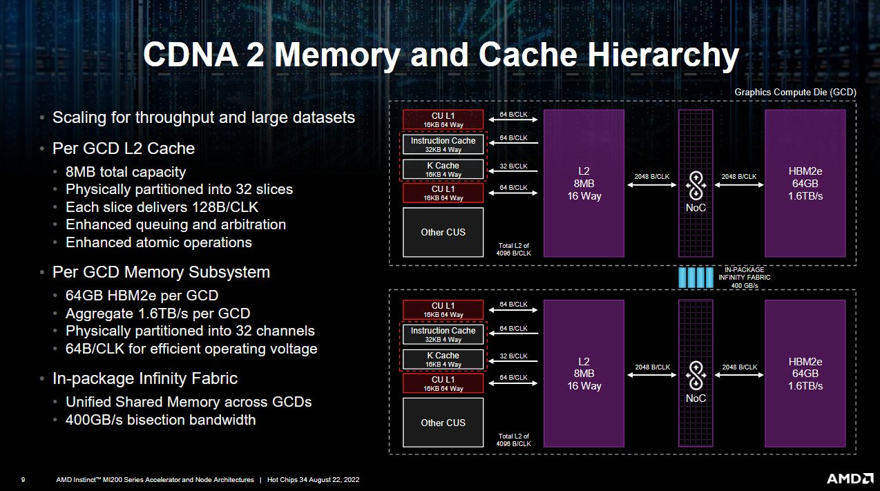
Latency for these first level caches is mediocre. The scalar cache does fine with 37.5 ns of latency, while the vector path is slower at just over 85 ns. Meanwhile, Nvidia’s H100 has a bigger and faster L1 cache. However, there is a catch because Nvidia uses one block of storage for both L1 cache and scratchpad (LDS or Shared Memory) storage. If you ask for a large scratchpad allocation, Hopper’s L1 caching capacity can decrease to 16 KB. But even in that case, Nvidia still enjoys a latency advantage.
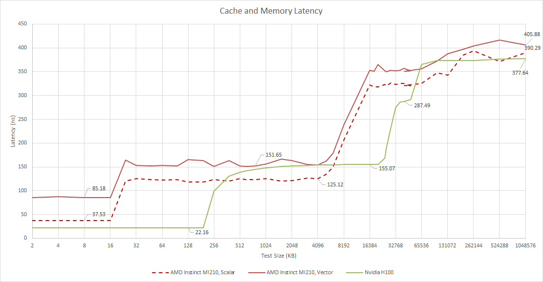
CDNA 2 and Nvidia’s Hopper both back their L1 caches with a multi-megabyte L2. AMD’s L2 is smaller, but can deliver lower latency for scalar accesses. L2 vector access latency is about the same on both architectures. Out in VRAM, both compute architectures see higher VRAM latency than graphics-oriented ones. But Nvidia’s H100 is slightly better than AMD’s MI210.
Advances over GCN
CDNA 2 retains GCN’s overall caching strategy, which means the cache setup is quite simple compared to what we see on AMD’s consumer graphics cards. However, AMD did make the vector cache a lot faster.

AMD’s Radeon RX 460 is a budget graphics card from 2016, and uses an iteration of the GCN architecture called Polaris. Scalar cache latency is very similar on both the MI210 and RX 460, but the RX 460 takes almost twice as long to get data from its vector cache. MI210’s vector latency improvement is welcome, and should improve execution unit utilization if L1 vector cache hitrates are high but occupancy is low.
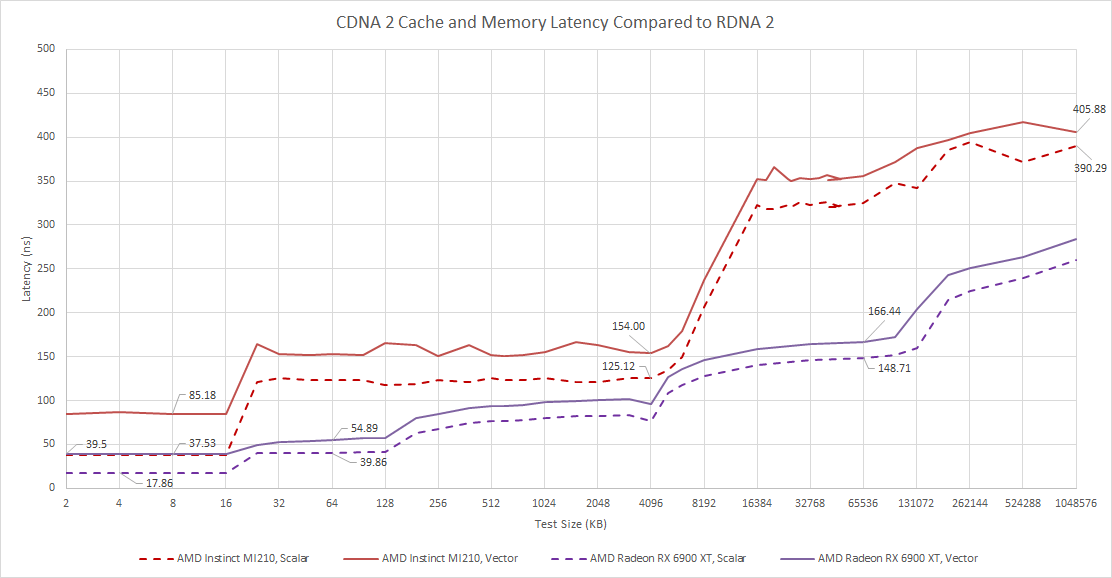
However, MI210 doesn’t go as far as RDNA 2 does. AMD designed RDNA to maintain good utilization even if a game throws a pile of small, dependent draw calls at it, and RDNA 2’s low latency cache hierarchy reflects that. Furthermore, RDNA 2’s large caching capacity lets it get by with a cheaper VRAM setup as long as cache hitrates are good. On the other hand, CDNA 2 can excel when given very large workloads, and maintain performance well if access patterns aren’t cache friendly.
Local Memory Latency
CPUs have global memory backed by DRAM, end of story. GPUs however have several different memory types. One of these is called “local memory” in OpenCL, and refers to a fast software managed scratchpad. AMD implements this with a block of memory called the LDS (Local Data Share), while Nvidia does so with what it calls Shared Memory. Because local memory is not a cache, it can potentially be faster because it doesn’t need to do tag and state checks to determine if there’s a hit. Software can also expect consistent, fast access to data stored in local memory. Compute applications can make pretty heavy use of local memory:

CDNA 2 enjoys much faster access to the LDS than to its vector cache, but it’s only a little bit faster than the scalar cache. It’s also faster than its GCN ancestors, but falls behind compared to both AMD’s gaming oriented architectures and Nvidia’s contemporary GPUs.

Atomics Latency
We can also test global and local memory latency for contested accesses by using OpenCL’s atomic_cmpxchg on those respective memory types. This is the closest we can get to a core to core latency test on a GPU. CDNA 2 turns in a pretty good performance if we’re using the LDS to bounce data between two threads running on the same compute unit. It pulls ahead of Nvidia’s A100 and isn’t too far off the H100. Just as with the local memory test, it’s a good step ahead of its GCN ancestors.

However, CDNA 2 again falls behind compared to consumer GPUs. AMD’s own RDNA 2 can handle local atomics with about half the latency. CDNA 2 seems to have good handling for atomic operations, but its LDS just isn’t that fast.
We can also use atomics on global memory to bounce data between threads that aren’t necessarily running on the same basic GPU building block. CDNA 2 pulls ahead of Nvidia’s H100 and A100 here. It’s a touch behind GCN, but that’s probably because the Renoir iGPU tested here is a particularly small GCN implementation. The Radeon VII has 140 ns of latency in the same test, so CDNA 2 improves on GCN if we restrict our comparison to larger GPUs.
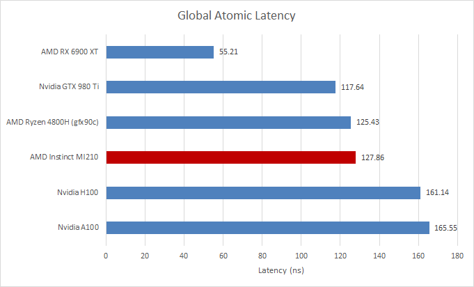
However, the MI210 falls behind client GPUs. I guess that’s expected because of how big CDNA 2 is. The die might be a bit smaller than Nvidia’s A100 or H100’s, but in the end there are still 104 CUs on that chip. Client GPUs tend to have fewer building blocks, and run at higher clock speeds. That reduces latency, leading to better performance with atomics.
Going back through some compute code, again with Folding at Home, I saw global atomics used in a few places.

These instructions aren’t exactly the compare and exchange ones I used to test latency with, but they should involve the same hardware.
Bandwidth
MI210’s L2 is shared across the entire GPU, so its bandwidth has to scale to keep everything fed. We got 3.7 TB/s out of it during testing. On its own, that’s impressive, but it falls behind H100’s and ends up closer to A100’s “far” L2 partition. AMD’s RX 6900 XT has similar L2 bandwidth. Curiously, AMD’s top end RDNA 2 card has similar FP32 throughput, so the two cards have very similar compute to L2 bandwidth ratios.
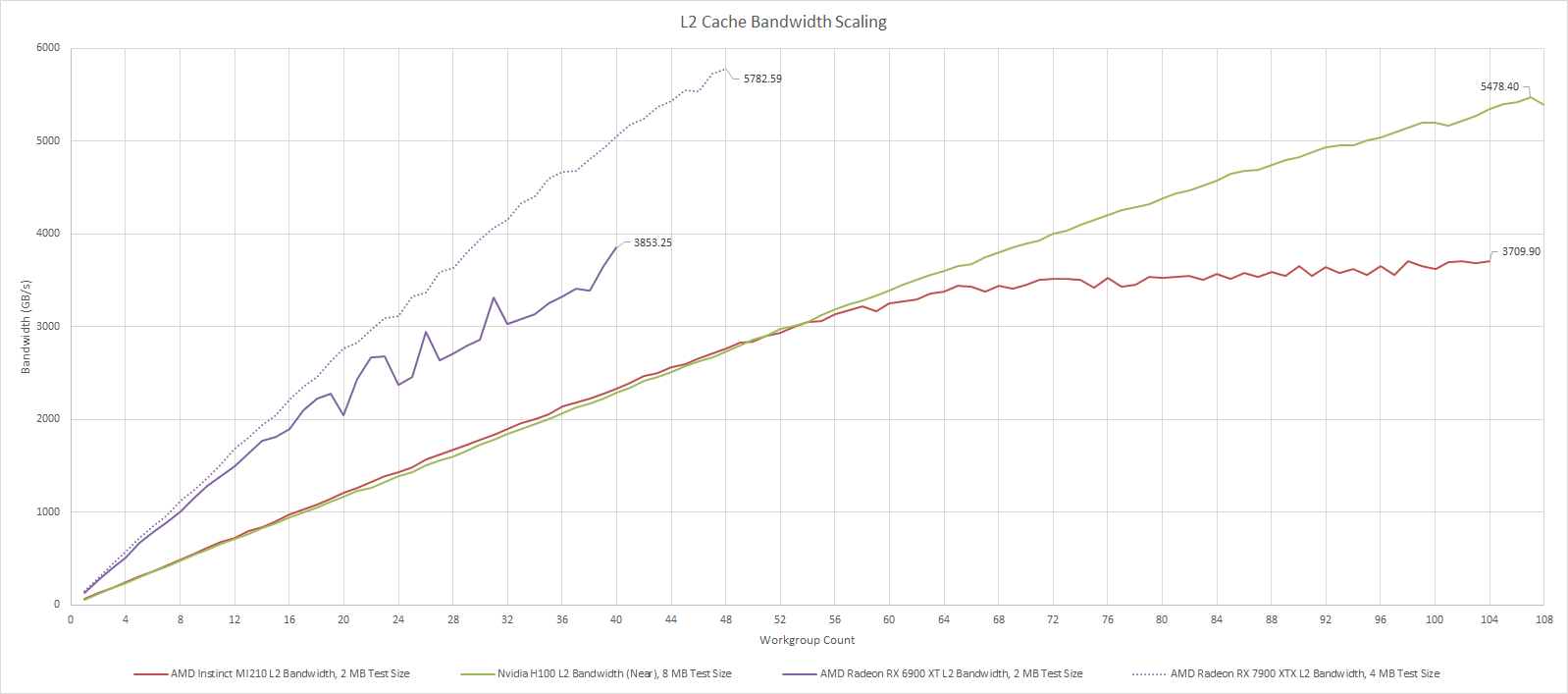
All threads in a workgroup have to run on the same SM (Streaming Multiprocessor), CU (Compute Unit), or WGP (Workgroup Processor), so the X axis indicates how many of those basic GPU building blocks are loaded. The MI210 shows almost linear scaling until about half the GPU is loaded, after which the curve flattens out. That suggests L2 bandwidth is limited by how many requests each CU can keep in flight up until 52-56 CUs are loaded. H100 and MI210 are very close up until that point. Both CPUs have about the same L2 vector access latency, so MI210’s CUs and H100’s SMs are probably keeping a similar number of L2 requests in flight. RDNA 2 benefits from a much lower latency L2 and therefore can get higher bandwidth with limited parallelism
Testing memory bandwidth is much harder because the memory controller can combine requests to the same addresses and satisfy them with only one read from DRAM. That appears to be happening with the MI210, and my bandwidth test produced an overestimate. I’ll have to address this, probably by making each workgroup read from a separate array if I ever have enough free time.

The MI210 should have 1.6 TB/s of memory bandwidth, putting it a bit behind the 2 TB/s available from the H100 PCIe’s memory subsystem. Whatever the case, both of these compute oriented GPUs have significantly more VRAM bandwidth available than contemporary gaming ones.
PCIe Link Bandwidth
CDNA 2 has a couple of options available when communicating with a host CPU. It can use a special Infinity Fabric interface that provides up to 144 GB/s of bandwidth between the GPU and CPU. Or, it can use a standard PCIe Gen 4.0 link. In our case, the MI210 uses the latter option.

The test system had two Genoa sockets exposed as two NUMA nodes, with the MI210 attached to node 1. CPU to GPU bandwidth did not vary significantly depending on which node the test was pinned to.
Even without an exotic Infinity Fabric link, the MI210 stands up well to Nvidia’s H100 PCIe card. When copying data to and from VRAM, AMD’s card was able to complete the transfers a bit faster.

Nvidia’s H100 should be pulling ahead because it has a PCIe Gen 5 interface. Lambda Cloud connected the H100 to an Intel Xeon Platinum 8480+, which also supports Gen 5. I’m not sure why the H100 isn’t beating the MI210.
Compute Units
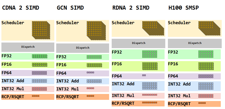
CDNA 2’s compute units are organized a lot like GCN’s. Both feature four 16-wide SIMDs and operate on 64-wide wavefronts. AMD names the architecture “gfx90a”, so the company considers it more closely related to GCN than to RDNA. For example, the Vega integrated GPU on Renoir APUs identifies itself as “gfx90c”, while the RX 6900 XT identifies itself as “gfx1030”.
Compared to GCN, CDNA 2 has been extensively modified to suit scientific applications and handles FP64 at full rate. A CDNA SIMD can execute 16 FP64 operations per clock, giving the MI210 a massive amount of FP64 throughput.
That’s a standout feature at a time when everyone else is focusing on lower precision thanks to the rapidly inflating AI bubble. Machine learning can get good-enough inferencing results with FP16 or even unsigned 8-bit integers. Losing a bit of accuracy is fine because AI is not expected to deliver perfect accuracy. For example, no one cares if some AI-assisted self driving cars go flying off the road and slam into things because cars do that every day anyway. However, other workloads need all the accuracy they can get. Floating point errors can accumulate with each step of a simulation, so using higher precision types can make scientists’ jobs a bit less painful.
In a bit of a surprise, CDNA 2 also does integer multiplication at full rate. For a while, Nvidia had best-in-class INT32 multiplication performance. Turing and Volta got what Nvidia confusingly called a dedicated INT32 datapath. It’s confusing because nearly every other GPU could do the more common INT32 adds at full rate, so Turing wasn’t generally ahead for INT32 operations. It was just better at multiplies, which could be done at the same rate as FP32 operations (because Nvidia also cut FP32 throughput per SMSP in half). Turing’s strong integer multiplication was carried forward and continued to feature on Ampere, Ada Lovelace, and Hopper. Those GPUs could do half-rate integer multiplication.

So CDNA 2 one-ups Nvidia. RDNA GPUs weren’t exactly bad at INT32 multiplication and could do them at quarter rate, but it seems like AMD found enough integer multiplication performance important enough for compute to invest heavily in it. I tested LuxCoreRender and Folding At Home on RDNA 2, and did see integer multiplication operations, so I guess AMD was on to something.
Lower Precision Ops
AMD may have prioritized higher precision, but they didn’t forget about FP32. CDNA 2 can do packed FP32 operations, which basically puts FP32 into the same class as FP16 on other GPUs. FP16 or FP32 operations can be done at double the nominal compute rate, assuming the compiler allocates registers in a way that lets that happen.

Compared to typical packed FP16 execution, packed FP32 execution is a bit weird because CDNA 2’s registers are still 32-bit. While packed FP16 puts two FP16 values in the two halves of a 32-bit register, packed FP32 execution uses adjacent 32-bit registers. It’s subject to the same register alignment restrictions as 64-bit operations, so you have to give the packed FP32 operation an even register address.
Packed FP32 execution gives CDNA 2 respectable FP32 throughput, though making use of that will be as difficult as making use of double rate FP16 execution on other GPUs. The compiler has to allocate registers properly and recognize packing cases. Thankfully, that all worked out for us:
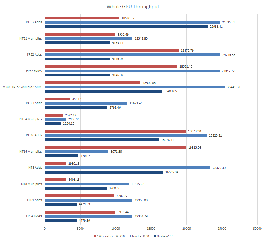
In the end, AMD’s MI210 is a substantially smaller GPU than Nvidia’s H100. It uses a smaller die and a cheaper 6 nm process, and isn’t a top-end product. However, the MI210 can occasionally punch harder than its vector lane count would suggest. FP64 and INT32 multiplication performance is very strong, and lands within striking distance of Nvidia’s H100. FP32 performance is similarly strong if packed operations come into play. In those categories, MI210 manages to pull ahead of Nvidia’s older A100, which is quite an achievement considering both use similar process nodes and A100 uses a bigger die.
But Nvidia’s high end products pull ahead in other areas. Everyone can do INT32 adds at a rate of one per vector lane, and Nvidia brings a lot more of those lanes to the game. Nvidia has a substantial advantage with very low precision integer operations because AMD doesn’t have packed INT8 instructions. Finally, Nvidia has made substantial investments into machine learning, and has very beefy matrix multiplication hardware. The H100 PCIe’s tensor cores can theoretically hit 756 TFLOPS with FP16, or double that with sparse matrices. AMD has worked tensor cores into CDNA 2, but they’re nowhere near as beefy. The MI210’s 181 TFLOPS of FP16 matrix compute offers a decent boost over using plain vector operations, but it’s nowhere near Nvidia. Unfortunately I don’t have any matrix multiplication tests. Maybe I’ll write one ten years later when there’s a standardized API for it and I have hardware with tensor cores.
Where Does MI210 Stand?
Now that we’ve had a decent look at CDNA 2’s architecture and goals, running a couple of benchmarks would be nice to see where the card stands for its intended workloads.
FluidX3D (FP32)
FluidX3D uses the lattice Boltzmann method to simulate fluid behavior. It features special optimizations that let it use FP32 and still deliver accurate results in “all but extreme edge cases”. I’m using FluidX3D’s built in benchmark.
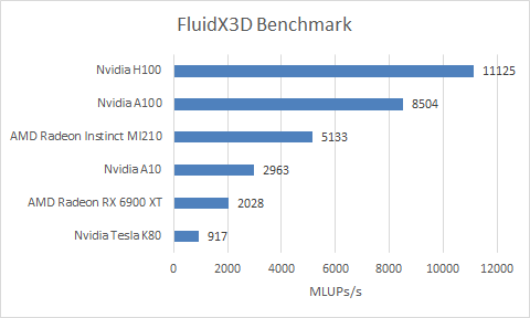
The MI210 falls quite short of Nvidia’s H100, and even the older A100. AMD’s compiler was unable to generate any packed FP32 operations in FluidX3D’s hottest kernel, called “stream_collide”. Packed FP32 operations were observed in other kernels, so the compiler was aware of them, but unfortunately could not use them where it mattered most.
In AMD’s favor, the MI210’s high memory bandwidth saves it against consumer GPUs. AMD’s Radeon RX 6900 XT and Nvidia’s A10 can deliver very high FP32 throughput without using packed operations. But at least on RDNA 2, FluidX3D was very bandwidth bound with memory controller utilization pegged at 99%. With HBM2E, MI210 can keep its execution units better fed, even if it can’t fully utilize its FP32 potential.
Calculate Gravitational Potential (FP64)
CGP is a clam-written test workload. It takes a map of column density and does a brute-force gravitational potential calculation, which could be used to identify “clumps” with star forming potential. Gravitational forces are very small across large distances, so FP64 is used to handle them. I spent about a day writing this and did not put effort into optimization. The code should be considered representative of what happens if you throw a cup of coffee at a high school intern and tell them to get cracking. To benchmark, I used a 2360×2550 image of the Polaris flare from the Herschel Space Observatory’s SPIRE instrument.

AMD’s MI210 and Nvidia’s H100 are nearly tied. Technically the H100 has a slim lead, but the big picture is that AMD’s GPU is punching well above its weight. Getting roughly the same level of performance out of a smaller die manufactured on a cheaper process is quite an achievement.

This type of workload is how AMD and Nvidia’s compute architectures can justify their existence and price tag. FP64 isn’t used in graphics, so consumer GPUs have been skimping on FP64 hardware in favor of maximizing FP32 throughput. That means they get absolutely crushed in FP64 tasks. Of the consumer GPUs I tested, AMD’s Radeon RX 6900 XT had the least terrible performance, finishing in just over 6 minutes. RDNA 2 is helped by its 1:16 FP64 ratio, and its Infinity Cache, which is large enough to hold the entire working set.

Nvidia’s A10 fares far worse. It can’t escape GA102’s terrible 1:32 FP64 ratio and takes 27 minutes to finish. Finally, AMD’s Polaris-based RX 460 does not do well, despite being given data from the area in space it was named after. It took over an hour to complete the task.
Final Words
For most of the 2010s, AMD relied on iterations of their GCN architecture. GCN offered lower latency and more consistent performance than the Terascale architecture that it replaced, but was often a step behind Nvidia’s graphics architectures. Maxwell and Pascal made that abundantly clear. GCN could sometimes compare favorably at higher resolutions where latency was less important and the large amount of work in flight could better feed GCN’s shader array. But by 2019, AMD decided their graphics architectures needed to be more nimble, and RDNA took over.
Compute workloads have different requirements. Folding at Home didn’t use particularly large dispatches, but other compute workloads do. LuxCoreRender consistently uses large enough dispatches to fill the 6900 XT’s shader array, with occupancy only limited by register file capacity. GCN was great at big compute workloads, and thus provided an excellent foundation for AMD to take a shot at the supercomputer market. AMD developed CDNA from GCN, and from CDNA, they developed CDNA 2. In contrast, Nvidia’s graphics and compute architectures tend to be built from the same generational foundation. Hopper shares more similarities with Ada Lovelace than to Kepler or Maxwell from the 2010s. And A100 is closer to client Ampere than any of Nvidia’s older architectures.
Both strategies have advantages. Nvidia sometimes enjoys better interoperability between its client and datacenter architectures. For example, A100 binaries can run on client Ampere, though with reduced FP32 throughput. Meanwhile, AMD can diverge their graphics and compute architectures more, and potentially make them better suited to their respective purposes.
Nvidia and AMD use different die size strategies too. CDNA 2 uses a bit of a small die strategy, and uses dual die configurations to compete with Nvidia’s top end. Dual GPUs never worked in the gaming world because of frame pacing issues. But the compute world is quite different. Frame latency doesn’t matter there. Furthermore, HPC applications typically use MPI (or similar APIs) to scale across multiple nodes anyway, so they should be able to naturally make use of a dual GPU card.
Obviously a dual GPU configuration will be more difficult to utilize than a single large one. But as we saw earlier, the single die MI210 can punch above its weight in certain categories when compared against Nvidia’s giants. The flagship MI250X with two dies should be quite a formidable opponent to Nvidia’s HPC offerings, even if it loses some efficiency from having to pass more data between GPUs.
Compute resources are the final and most important strategic difference. AMD has invested heavily in FP64 compute and integer multiplication performance. The company is clearly prioritizing scientific applications. Put that next to the small die strategy, and AMD’s intention is clear. Nvidia’s relentless pursuit of AI performance has left a weakness in market segments that want high FP64 throughput. AMD wants to drive a truck through that hole.
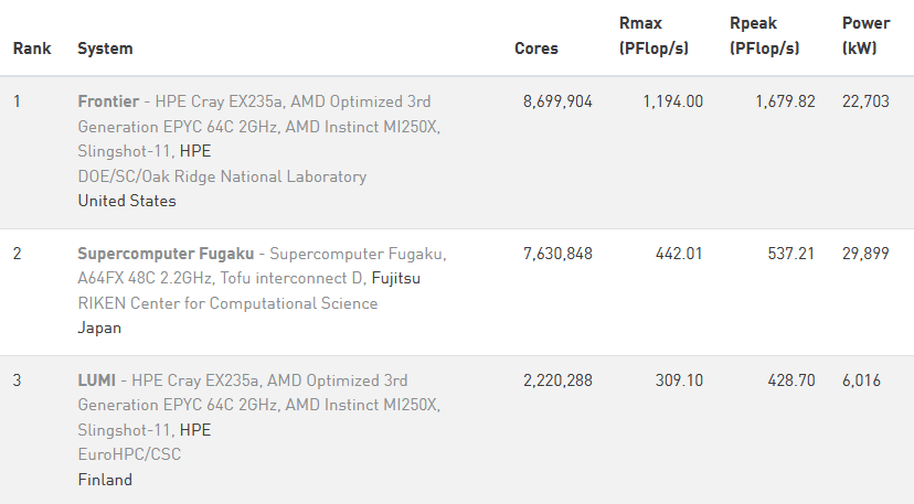
So far, that effort is successful. ORNL’s Frontier uses AMD’s MI250X, and is first place on TOP500’s June 2023 list. Of the 20 highest ranked supercomputers on that list, five use AMD’s MI250X. Large MI250X deployments thus also include Microsoft Azure’s Explorer in the United States, EuroHPC/CSC’s LUMI in Finland, GENCI-CINES’s Adastra in France, and Pawsey Supercomputing Centre’s Setonix in Australia. Nvidia’s H100 only has a single slot in the top 20, which belongs to the Eos supercomputer in rank 14. That’s Nvidia’s in-house supercomputer, so AMD’s offering would not have been considered for that deployment anyway.
Nvidia may be the leading incumbent in the HPC space, for now. A100 occupies eight of the top 20 slots, and V100 accounts for another three. But CDNA 2 has given AMD a strong foothold in the supercomputing market, with notable share in recently built systems. Hopefully they can continue the trend with future CDNA iterations.
If you like our articles and journalism, and you want to support us in our endeavors, then consider heading over to our Patreon or our PayPal if you want to toss a few bucks our way. If you would like to talk with the Chips and Cheese staff and the people behind the scenes, then consider joining our Discord.
Credits
We would like to thank the folks who set us up with a MI210 system. CDNA 2 is a fascinating architecture, and we wouldn’t have been able to investigate it otherwise.