
Hot Chips 34 – AMD’s Instinct MI200 Architecture


It’s no secret that AMD has been slowly but surely executing on their plans to achieve leadership in all domains of computing. On both the server CPU and consumer sides, we have seen them break into the space with Zen and RDNA – two great designs that have both been iteratively improved on with each generation. Today we take a look at their latest entry into the server GPU space: the Instinct MI200 architecture.
With the slowing down of Moore’s Law, and the ever growing processing needs of modern workloads starting to overtake the rate of generational performance increase, design houses have been forced to move to specialized, domain-specific architectures over more general one-size-fits-all approaches. In the GPU side, this has manifested in the divergence of gaming and compute architectures, with RDNA as the lean, latency optimized architecture tackling graphics and gaming workloads, and CDNA as the throughput optimized architecture to take on compute workloads. The MI200 is the second entry in the CDNA family, replacing the MI100 before it.
While from a higher level glance, the MI200 may seem to be a regular iterative improvement over its predecessor in key areas; reinforcing some of the MI100’s weaknesses, and improving on its strengths, arguably, the MI200 marks a new era for AMD’s server GPGPU designs, and the point when they begin using their advantage as a strong CPU and GPU designer. By leveraging key technologies such as their Infinity Fabric interface, AMD has managed to create a coherent memory space between their CPUs and GPUs, offering a great advantage in certain workloads.
Not just that, but through the Infinity Fabric, AMD gets to tackle chip scaling issues by using a chiplet approach ala Zen, where a chip package would contain multiple graphic chiplets, and each of the graphic chiplets is connected to another through Infinity Fabric links.
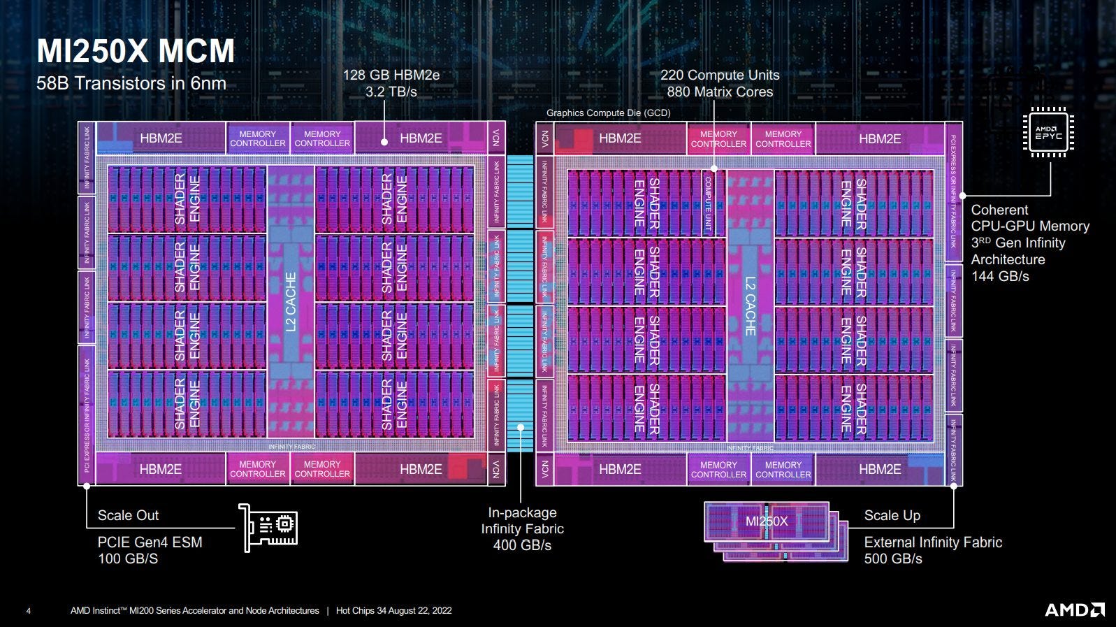
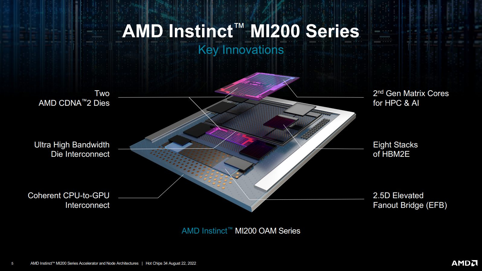
In fact, the two main MI200 accelerators (MI250, MI250X) use this approach, where each accelerator is composed of two chiplets (“GCDs” – Graphics Compute Dies) connected to each other by coherent 4x Infinity Fabric links, allowing flexibility and scalability by using multiple smaller-sized, better yielding GCDs rather than one large monolithic chip. As expected with the first gen of a new technology like this, however, it comes with multiple caveats.
First, from a software perspective, a single accelerator is exposed as two separate GPUs. This means that your algorithm needs to be multi-GPU aware in order to fully utilize the accelerator. Second, despite being connected by 4 high-speed IF links, the chip-to-chip bandwidth is still much lower than the HBM memory bandwidth, leading to moving data between GCDs being rather painful, and significantly slower than memory accesses. This is actually the reason AMD opted to expose the accelerators as two distinct GPUs; they couldn’t match the HBM bandwidth between the two dies to be able to expose both GPUs as one, nor at least half of it to support a distributed mode configuration, so they decided to expose them as different GPUs.
Interestingly enough, two other Hot Chips presentations showcased multi-die GPUs that could present themselves as one unified GPU. Intel’s Ponte Vecchio could so, as could Biren’s BR100. Just as NUMA-aware software can perform better when a multi-CPU system is set to NUMA mode (showing multiple memory pools), software aware of a multi-die GPU’s topology will be able to get the most out of the hardware. But for software that isn’t “NUMA-aware”, Intel and Biren’s GPUs can pretend to be a single GPU, allowing software to get some scaling.
In AMD’s favor, this disadvantage won’t be much of a factor in HPC environments. HPC code is designed to scale across multiple nodes by using MPI to synchronize and pass data over high speed networks. The dual die MI250X would simply be treated as two GPUs with a particularly fast link for message passing between them. Multi-GPU setups are pretty common in supercomputers even if we exclude MI250X based systems. For example, Summit nodes pack six GV100 GPUs in each node, while Perlmutter‘s GPU enabled nodes have four A100 GPUs each. Simply put, if you can’t write code that scales well over several GPUs for some reason, it’s probably not a good fit for a supercomputing cluster.
Compute – A Peek Inside the MI200 GCD
Moving on, we take a look at the MI200 GCD, and the improvements it brings over the MI100.
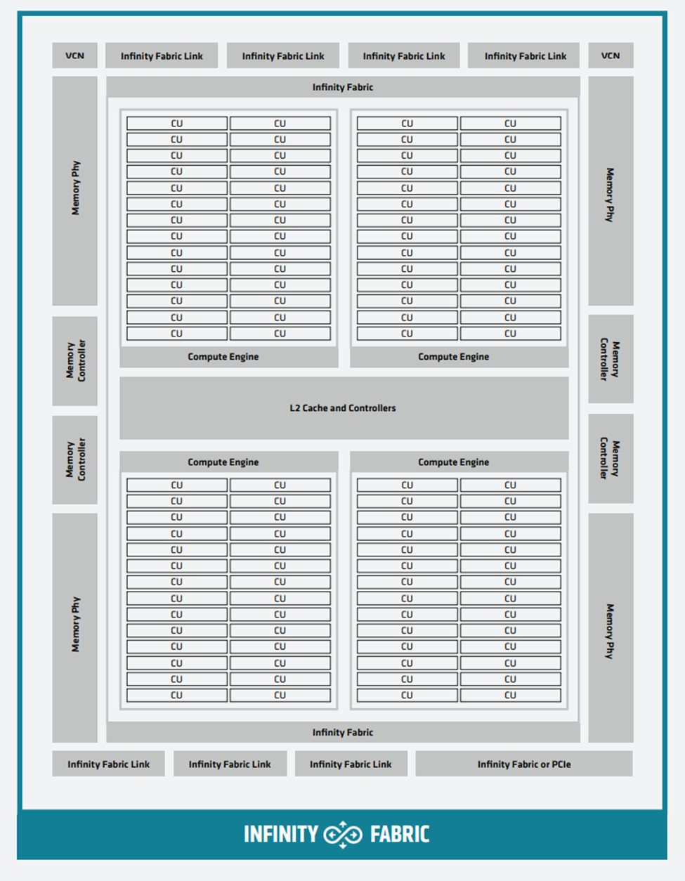
Overall, the compute architecture of the MI200 GCD takes an iterative, evolutionary approach over the previous architecture of the MI100. The die is split into 4 compute engines, each fed by an Asynchronous Compute Engine, with each compute engine divided into 2 shader engines, and each shader engine having 14 Compute Units (CUs).

The structure of the CUs remains largely the same as the MI100. Each CU has 4x SIMD16 units and 4x Matrix Core units, with a scheduler, a 16KB 64-way L1 cache with 64B/CU/clk bandwidth, Load/Store units, and the local data share. The main difference here is that the ALUs are now natively 64-bit wide. This means that the MI200 can do full-rate FP64, which is not only a 2x increase in throughput relative to the MI100, but also a sizable advantage against the NVIDIA A100 and puts the MI200 accelerators just slightly worse than the next generation NVIDIA H100 in FP64.
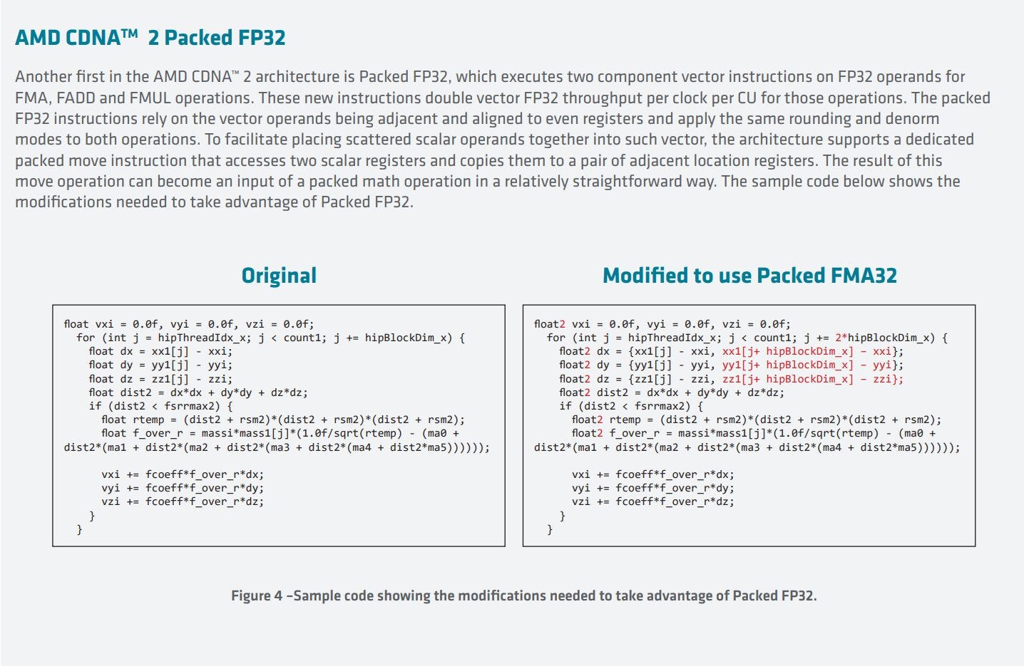
AMD has also used this capability to provide support for packed FP32 instructions, which enables twice the throughput for some FP32 operations (FMA, FADD, and FMUL). However, this does not come for free – it requires code modification in order to work, as the operands need to be both adjacent and aligned to even registers. AMD also includes dedicated packed move instructions to help with sorting scattered operands so that they can be used with packed FP32 operations. Register assignment is of course the compiler’s job and not the programmer, however with packed FP32, the compiler needs to be guided in order to utilize this functionality, necessitating some modification.
While the required code changes may seem disappointing, it’s slightly less of an issue for the supercomputer platforms the MI200 targets, where specially written software is more tolerable.
Starting with the MI100, AMD added matrix units to their CUs. Like NVIDIA’s Tensor Cores, these matrix units are accessed via a set of new instructions. On both NVIDIA and AMD, matrix instructions break the SIMT abstraction model and work across a whole wavefront (or “warp” on NVIDIA).
Matrix ops are also a tad weird on both sides. NVIDIA relies on a special layout in the vector register file. AMD adds a second accumulator register file. For an A * B + C matrix operation, a MFMA instruction can take A and B from either register file, but C must come from the accumulator register file.

CDNA2 improves on this by dropping the separate accumulator RF, opting to provide one big unified register file instead. Previously in the MI100, each SIMD16 unit had 256 “Architectural” Vector General Purpose Registers (VGPRs) for itself, with the Matrix Core Unit having another 256 “Accumulator” registers. The MI200 combines both of these into a single unified register file with 512 entries. For matrix operations, this removes the potential hassle of moving values between the register files to ensure the accumulator input could come from the accumulator register file. The unified register file’s increased entry count can also help reduce register pressure and potentially increase occupancy when running non-matrix code as well.

The Matrix Core Unit in the MI200 also gets support for full rate FP64, leading to a 4x increase in FP64 FLOPS per CU cycle against the MI100. Lower precision matrix math sees throughput increases too, with BF16 throughput per CU clock doubling relative to the MI100. Moreover, more power efficient matrix instructions for 16x16x4 and 4x4x4 blocks were introduced.
Lastly, the LDS in the MI200 CU gets improved atomics, and support for FP64 atomics.
These changes reflect and reinforce the HPC-focused approach that AMD is taking with their server GPUs, with a very strong focus on double precision vector performance over lower precision or matrix performance. The MI250X’s matrix units are improved over the ones in CDNA1, but it still only matches NVIDIA’s throughput per CU/SM clock with FP64. NVIDIA still offers higher matrix throughput when dealing with lower precision formats, making Hopper a much better choice for ML and AI workloads.
Memory Hierarchy – Scaling Up
Each GCD has an 8MB 16-way L2 cache, physically partitioned into 32 slices, with a BW of 128B/clk/slice, for a total bandwidth of 4096B/clk, which is effectively double the L2 bandwidth of the MI100. As with the LDS, L2 atomics were also enhanced with the MI200, with support added for FP64 atomics.
On the memory side, each MI200 GCD gets 4-stacks worth of 64GB 3.2 Gbps HBM2E, physically partitioned to 32 channels, with a bandwidth of 64B/clk at efficient voltages, which translates to 1.6 TB/s memory bandwidth per GCD, which is a 33% increase in bandwidth over the MI100, and a 100% increase in memory capacity. As the majority of workloads are memory bandwidth bound, these are good steps in the right direction, and for HPC in particular, the doubling of memory capacity will come useful as a large group of workloads is still memory capacity bound.

Compared to CDNA, a CDNA2 GCD brings slightly fewer CUs, but feeds those CUs with a lot more cache and memory bandwidth. This bandwidth increase was probably necessary because CDNA2 compute units can handle FP64 at full rate, and FP64 values consume twice as much memory and memory bandwidth as FP32.
AMD’s HPC and consumer GPU architectures have increasingly diverged over the past few years, and CDNA2 and RDNA2’s memory subsystems could not be more different. While RDNA2 combines a cheap 256-bit GDDR6 setup with a very sophisticated cache hierarchy, CDNA2 has a simple two-level caching setup with massive L2 and DRAM bandwidth. CDNA2’s L2 actually has more theoretical bandwidth than RDNA’s L2, despite being larger.
NVIDIA’s caching approach is the opposite of AMD’s, while emphasizing high DRAM bandwidth in both consumer and HPC cards. Their consumer GA10x chips feature up to 6 MB of L2 and use a very high power, high bandwidth GDDR6X setup. In contrast, their HPC oriented A100 has 40 MB of L2, backed by HBM2. NVIDIA’s incoming Hopper architecture continues this trend and brings 50 MB of L2 backed by HBM3.
Connectivity – Infinity Architecture 3
High speed connectivity is what separates a supercomputer from any old pile of commodity hardware. HPC programs are designed to scale across many nodes, and do so by passing messages between nodes (with APIs like MPI). Fast links are therefore critical to ensuring good scaling. HPC clusters also need complex link topologies to provide as much bandwidth as possible between any two nodes, while minimizing the number of links needed. MI250X introduces a much more sophisticated IF link setup to maximize bandwidth whenever possible.
To start, AMD slightly increased IF link bandwidth. MI100’s IF links were 16 bits wide in each direction and ran at 23 GT/s, providing 46 GB/s of bandwidth in each direction, or 92 GB/s total. MI250X’s IF links remain 16 bits wide, but transfer rate is increased to provide 50 GB/s in each direction, or 100 GB/s total. Then, AMD implemented more IF links with different types of physical interfaces to maximize bandwidth within physical constraints. Four IF links have in-package interfaces, letting the two GCDs within a package talk to each other with 400 GB/s of bandwidth.
Three other IF links have inter-package interfaces, and are used to communicate with other GCDs and the host CPU. Unlike MI100, where three IF links per GPU allowed a fully connected quad GPU setup, MI250X requires a more complicated topology. Because each MI250X card is basically a dual GPU board, a quad GPU HPC setup needs to connect eight GCDs. AMD gives each GCD a direct link to two GCDs in peer MI250X cards. When cross-GCD communication does require an extra hop, that extra hop can always go through a high bandwidth in-package link. That avoids creating congestion on the lower bandwidth inter-package links.
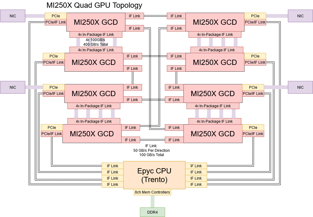
AMD uses the GCD’s third inter-package IF link to connect to the CPU. This link only operates in IF mode with a specially optimized 3rd gen EPYC CPU (the AMD Trento platform used in Frontier). This allows full coherency between both the CPU and GPU, where the CPU caches both its memory and the HBM memory in the MI250X, giving the MI250X package a major advantage in some workloads over other conventional setups. When connected with any other regular x86 CPU, the link behaves as a regular PCIe x16 interface.

Another major change with the MI200 is the addition of a downstream 25Gbps PCIe 4.0 ESM link. This downstream interface is coupled to a PCIe root complex, giving the GPU an ability to drive I/O devices that are connected to it. Thus, the GPU can manage devices connected to it directly, without having to rely on the CPU for management. This capability is especially useful with very high bandwidth network cards seen in supercomputing clusters. Traffic moving to and from IO devices is generally backed by DRAM, meaning that moving a lot of data through the network controllers could eat up a lot of DRAM bandwidth. Directly connecting NICs to MI250X GPUs allows AMD to back network traffic with the GPU’s HBM memory, which has a lot more memory bandwidth than the CPU’s DDR4.
This in turn makes a HPC setup with four 200 Gbps NICs practical, providing high bandwidth to other computers within a HPC cluster. If you tried to attach those four 200 Gbps NICs to the CPU, network traffic could eat up a large portion of CPU DRAM bandwidth, leaving it bandwidth starved if you wanted to do heavy compute on the CPU cores as well.
MI300 – Building On Solid Foundations
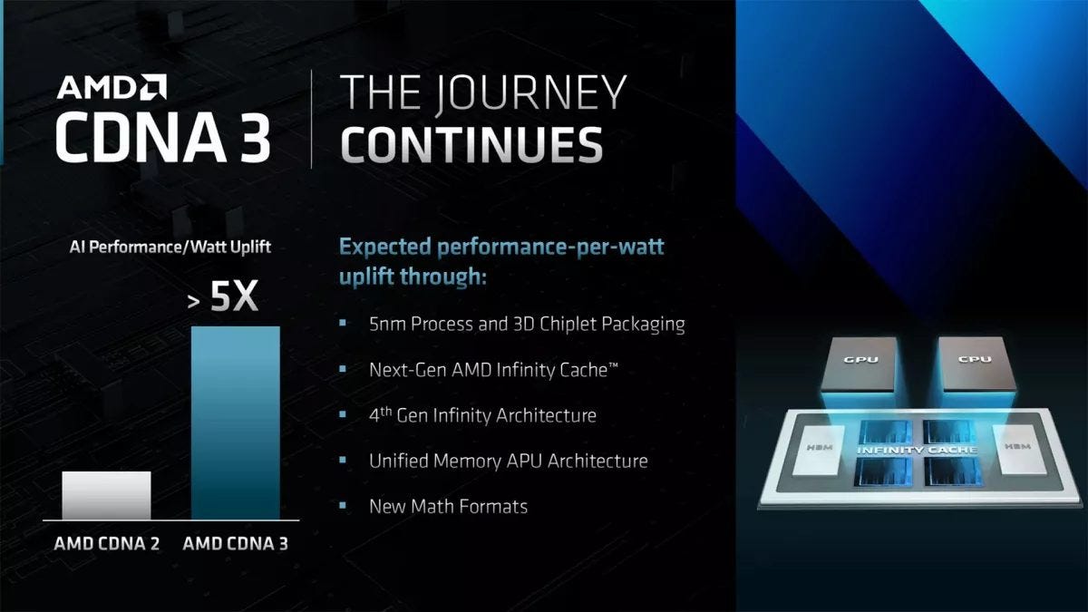
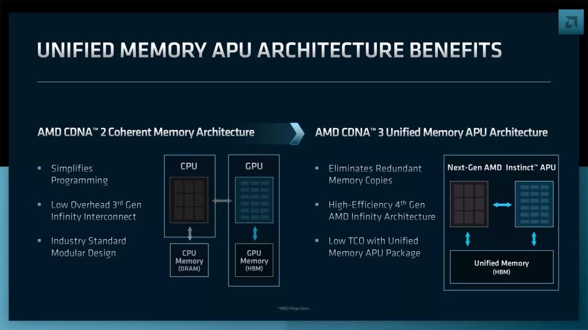
During AMD’s Financial Analyst Day, AMD disclosed the successor to CDNA2 which is unsurprisingly called CDNA3. CDNA3 looks to be a very different beast compared to CDNA 2, and continues the specialization for compute started by CDNA 1.
According to this slide, CDNA3 is not a standard GPU but is more like a very large and very powerful APU with CPU and GPU compute chiplets on the same package. It therefore continues the trend of improving CPU to GPU communication.

This is a natural next step after after the MI200. We’re going from having CPUs and GPUs working together as peers in a system, to getting CPUs and GPUs into the same package with a unified memory architecture.
Packaging the CPU and GPU together opens up even more possibilities, and it looks like AMD is considering Infinity Cache. RDNA 2 used Infinity Cache to avoid an expensive GDDR6X or HBM memory configuration. In CDNA3, a large, memory attached cache could provide several advantages. CDNA (and GCN generations) never had a particularly large L2 cache. Even with CDNA2, the L2 cache continues to be smaller than that of NVIDIA’s A100. Infinity Cache could bring a successful technique from RDNA2 over to the CDNA line. And Infinity Cache could accelerate copies between the CPU and GPU, since both would be clients of that cache. Finally, high bandwidth network cards can be attached to either the CPU or GPU, and IO traffic would be backed by the high bandwidth Infinity Cache + HBM setup.
HSA Lives Again?
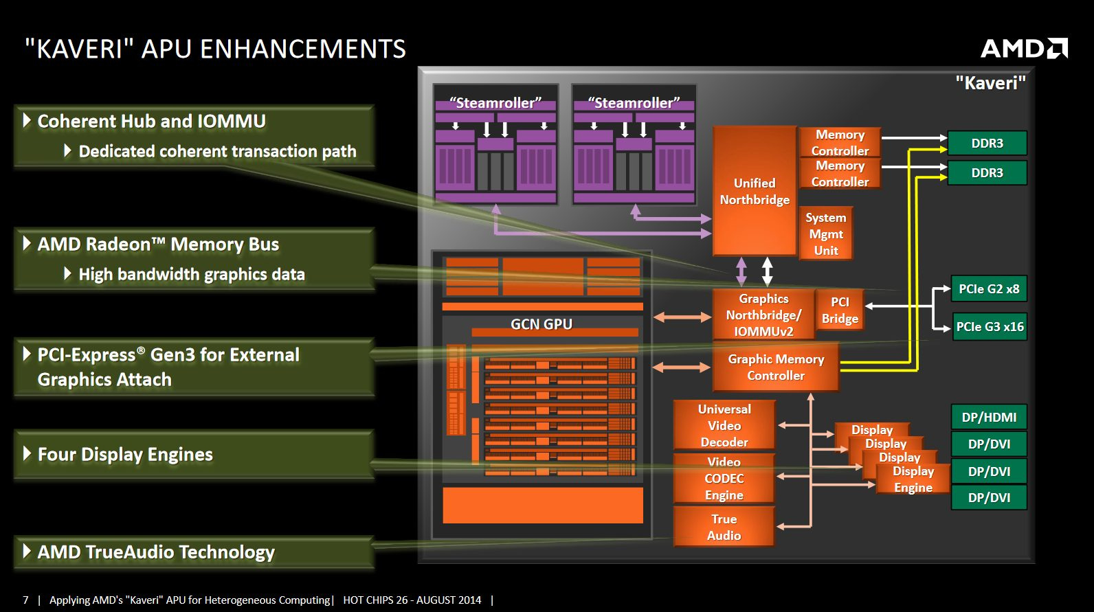
Many, many years ago, AMD introduced HSA (Heterogenous System Architecture) in its consumer APUs. AMD at the time had a serious processing power deficit compared to Intel. AMD’s vector units were 128-bits wide, while Intel had full-width 256-bit AVX units. Piledriver, Steamroller, and Excavator also shared a FPU between both threads in a module. However, AMD did have very strong graphics IP, so they hoped to compensate on this by packing a relatively powerful integrated GPU into their APUs. HSA would hopefully let compute applications take advantage of the APU’s unified memory pool and hardware coherency to utilize AMD’s iGPU throughput.
Sadly, AMD’s integrated GPUs were far weaker than discrete ones, so iGPU compute never really took off. However, iGPU compute is back with CDNA3 as are HSA benefits. CDNA3 should still be targeted at high performance compute, and should have enough performance to compete with discrete GPUs.
Putting the CPU and GPU on the same memory pool largely removes the need to copy data between the two devices. Instead, pointers can be passed around. The same physical memory pages can be mapped on both devices, without worrying about one device having to access that page over a low bandwidth link.

In summary, CDNA3 continues CDNA’s trend of specializing for compute applications, but it brings in techniques originally developed for consumer graphics architectures when they’re applicable for high performance compute.
Packaging and AI
Another big change that seems to be coming with the MI300 as well is Infinity Architecture 4, which looks to expand Infinity Architecture support to 2.5D/3D chiplets among other connectivity changes, which goes hand-in-hand with enabling the unified memory architecture the MI300 is bringing, as it will allow all the chips and chiplets within a single package to share a coherent and unified memory space.
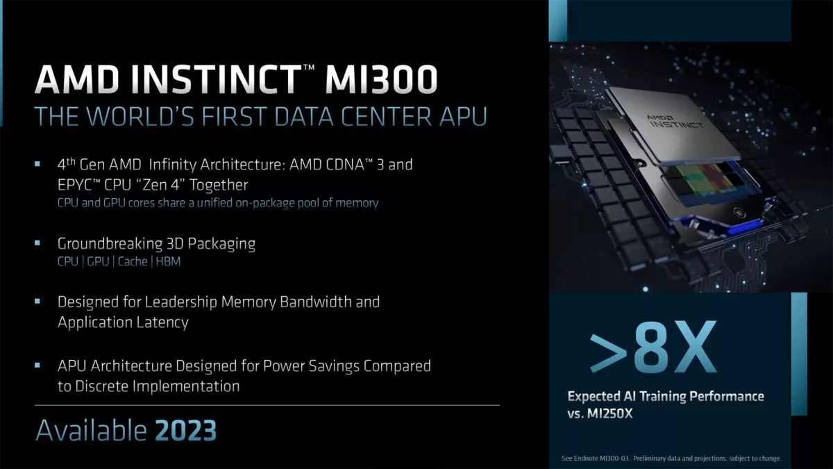
Last but definitely not least, the MI300 seems to also address one of the MI200’s core weaknesses, that being the relatively poor AI performance compared to the NVIDIA A100 and H100 architectures. With a claimed >8x estimated AI training performance, and >5x AI perf/watt uplift, it seems that AMD is going to give the matrix cores a decent upgrade. We also know that the MI300 will have support for FP8 from the endnotes, so lower precision performance looks to be getting focus, which would help with AI performance as well.
Conclusion – The Journey to Exascale
In mid 2022, we’re more than a decade away from AMD’s original GCN launch. A few years ago, AMD made major changes to GCN’s fundamental architecture to create RDNA, which provided massive efficiency benefits for graphics workloads. But GCN didn’t ride away into the sunset with RDNA’s rise. It was still very well suited to compute workloads, so AMD cut the G (graphics) out of GCN and started optimizing the architecture for high performance compute, giving us CDNA.

With the second generation of CDNA, the architecture steps even further away from its roots as a graphics oriented design. FP64 was practically irrelevant in the consumer graphics market, but is a first class citizen on CDNA2. Instructions for texture sampling with different levels of detail (LOD) were present in CDNA, but dropped with CDNA2. CDNA2 gets beefier matrix units as well, which AMD has no use for on the consumer graphics side.
AMD’s HPC focus is also reflected in the dual die design. CDNA2’s cross-die link lacks the bandwidth necessary to expose a unified pool of memory across both dies. Multi-GPU cards have just about died out in the consumer graphics space thanks to frame pacing issues. But HPC code is multi-GPU aware almost by definition, so MI250X’s multi-die design isn’t much of an obstacle while providing excellent compute density.
All of this specialization for the HPC scene has allowed AMD to deliver a package that was effectively unmatched by anything else for HPC, which has landed impressive supercomputer wins for AMD. Frontier and LUMI both pack MI250X GPUs, and occupy the first and third spots respectively on June’s TOP500 list. We look forward to seeing the MI250X make its presence felt on the market, though we suspect it’ll have a harder time dominating outside the HPC sector.
If you like our articles and journalism and you want to support us in our endeavors then consider heading over to our Patreon or our PayPal if you want to toss a few bucks our way or if you would like to talk with the Chips and Cheese staff and the people behind the scenes then consider joining our Discord.
 | A guest post by
|