
Nvidia’s H100: Funny L2, and Tons of Bandwidth

GPUs started out as devices meant purely for graphics rendering, but their highly parallel nature made them attractive for certain compute tasks too. As the GPU compute scene grew over the past couple decades, Nvidia made massive investments to capture the compute market. Part of this involved recognizing that compute tasks have different needs than graphics tasks, and diverging their GPU lineup to better target each market.
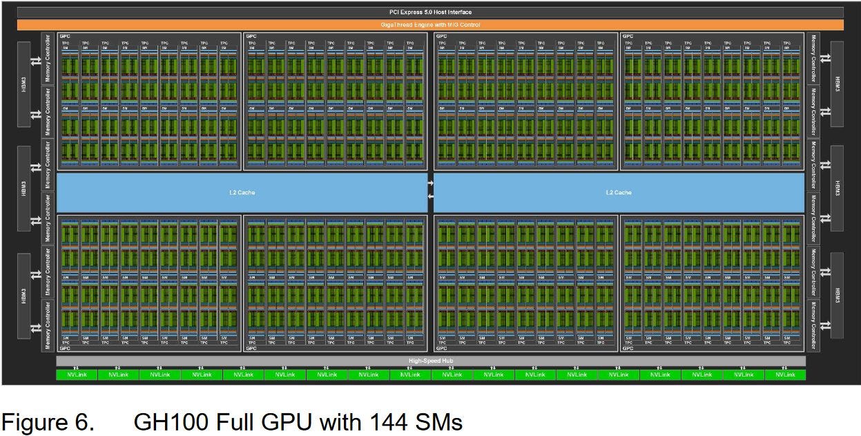
H100 is the latest member of Nvidia’s line of compute-oriented GPUs. It uses the Hopper architecture, and is built on a massive 814 mm2 die using TSMC’s 4N process with 80 billion transistors. This giant die implements 144 Streaming Multiprocessors (SMs), 60 MB of L2 cache, and 12 512-bit HBM memory controllers. We’re testing H100’s PCIe version on Lambda Cloud, which enables 114 of those SMs, 50 MB of L2 cache, and 10 HBM2 memory controllers. The card can draw up to 350 W.

Nvidia also offers a SXM form factor H100, which can draw up to 700W and has 132 SMs enabled. The SXM H100 also uses HBM3 memory, providing additional bandwidth to feed those extra shaders.
Brief Note on Clock Speeds
The H100 features a much higher boost clock than the A100. When microbenchmarking, the H100 occasionally dropped down to as low as 1395 MHz, or just under 80% of its maximum boost clock. Other metrics from nvidia-smi suggest we could be hitting a power limit, particularly when pulling data from L2. The H100 PCIe version has a power limit of 350W, and gets right up against that when bandwidth testing.

Server cooling is able to keep the H100 at a very low temperature, even when the GPU is sucking down over 300W. Memory temperatures are a bit higher, but still well within reason.
A100 saw different behavior. Core clocks went to 1410 MHz under load and stays there. Power draw is also quite high, but the SXM4 version of A100 has a higher 400W power limit. Probably because of that, we don’t see any clock speed drops even as power draw passes 350W.
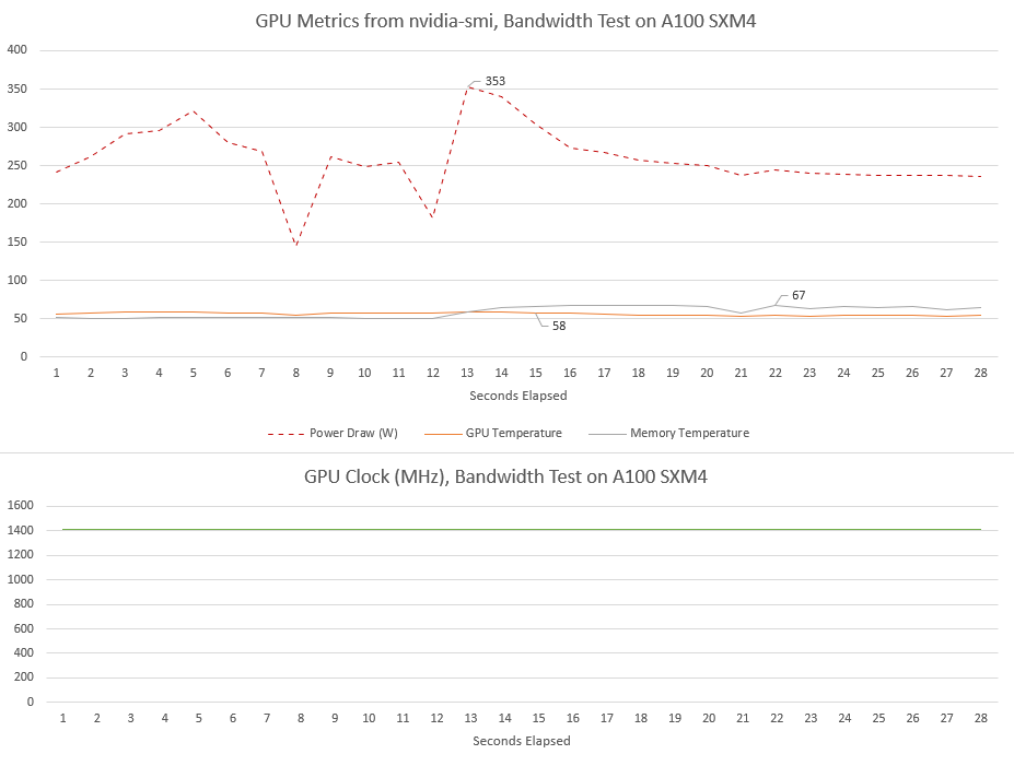
Like H100, A100 enjoys very low core temperatures. Passively cooled cards seem to thrive in a server chassis with plenty of airflow. A100’s memory temperatures are also lower than H100’s.
Cache and Memory Setup
Computers have been limited by memory speed for just about all of eternity. We’ve seen consumer GPUs counter this with increasingly sophisticated cache setups. AMD’s RX 6900 XT used a four level cache hierarchy with 128 MB of last level caching capacity, while Nvidia’s RTX 4090 extended L2 capacity to 72 MB. Nvidia’s compute GPUs have seen increased caching capacities too, but the strategy there is a bit different.
Streaming Multiprocessors (SMs) are Nvidia’s basic GPU building block. Nvidia has consistently emphasized SM-private caching in prior datacenter oriented GPUs. For most Nvidia architectures, a SM has a private chunk of memory that can be flexibly partitioned between L1 cache and Shared Memory (a software managed scratchpad) usage. GK210 Kepler SMs had 128 KB of memory for that compared to 64 KB on client implementations. A100 had 192 KB compared to 128 KB on client Ampere. Now, H100 brings L1/Shared Memory capacity to 256 KB.
We can do limited testing of L1 cache allocations by using Nvidia’s proprietary API. We usually test with OpenCL or Vulkan because many vendors support those APIs, letting tests run unmodified across a large variety of GPUs. But CUDA gives limited control over L1 and Shared Memory splits. Specifically, we can ask the GPU to prefer L1 caching capacity, prefer an equal split, or prefer Shared Memory capacity. Asking for larger L1 cache allocations doesn’t come with any latency penalty.
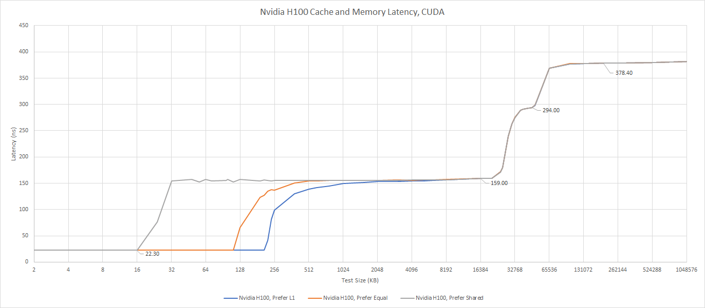
When we ask CUDA to prefer L1 caching capacity, we see 208 KB of L1 cache. With this setting, H100 has more first level data caching capacity than any other GPU. Even if we account for AMD’s strategy of using separate memories for caching and scratchpad purposes, H100 continues to be ahead. Adding up RDNA 3’s L0 vector cache, scalar cache, and LDS (scratchpad) capacity only gives 208 KB of storage, compared to 256 KB on Hopper.
Against A100, H100’s L1 is both higher capacity and lower latency. It’s a welcome improvement, and the trend of being slightly better than A100 continues further down the cache hierarchy.
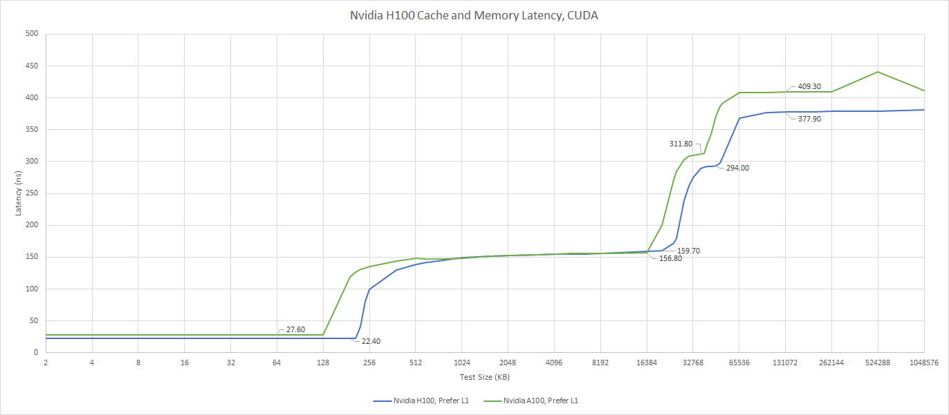
For data that can’t fit within L1, H100 has a 50 MB L2. When A100 launched in 2020, its 40 MB L2 gave it more last level caching capacity than any Nvidia GPU at the time. H100 slightly increases cache capacity, but it’s nothing special today. Nvidia’s RTX 4090 features 72 MB of L2, while AMD’s high end RDNA 2 and RDNA 3 GPUs have 128 MB of 96 MB of last level cache respectively.
H100 also inherits A100’s split L2 configuration. Any thread running on the GPU can access the full 50 MB of cache, but not at the same speed. Accessing the “far” partition takes nearly twice as long. It has about as much latency as VRAM on the RX 6900 XT, making it more useful for bandwidth than for getting individual warps or wavefronts to finish faster.

H100’s L2 cache feels like a two-level setup rather than a single level of cache. A thread running on H100 can access the “far” L2 cache a bit faster than on A100, so Nvidia has improved compared to the prior generation. A100 was a bit of a pioneer for Nvidia when it came to implementing large caches, and H100’s setup is a natural evolution of A100’s. But this isn’t the low latency, efficient cache setup used on modern client GPUs.
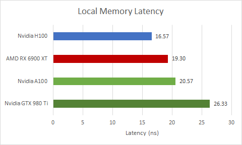
Out in VRAM, H100 sees slightly lower latency than A100, and is comparable to some older client GPUs. For example, the GTX 980 Ti has about 354 ns of VRAM latency.
No More Constant Cache?
Nvidia has long used a separate constant cache hierarchy, typically with a 2 KB constant cache backed by a 32 to 64 KB mid-level constant cache. The constant cache offers very low latency access, but is read-only and backed by a limited memory space. H100 handles constant memory differently. Nvidia can allocate up to 64 KB of constant memory (a limitation dating back to the Tesla architecture), and latency is constant throughout that range.

Furthermore, latency looks nearly identical to L1 cache latency. H100 might be using the L1 data cache to hold constant data. Validating this assumption would require additional testing that I can’t currently make the time investment for, due to real life and day job demands. But whatever Nvidia did, it provides a clear improvement over A100’s constant caching, with lower latency across the board. Ada Lovelace enjoys lower latency if it can serve requests from a tiny and fast 2 KB constant cache, but also falls behind if there’s a lot of constant data.
Local Memory Latency
As mentioned before, H100’s SMs have a large block of private storage that can be split between L1 caching and Shared Memory use. Shared Memory is Nvidia’s term for a software managed scratchpad that offers consistently high performance. AMD’s equivalent is called the Local Data Share (LDS). On Intel GPUs, it’s called Shared Local Memory (SLM). OpenCL refers to this memory type as local memory.
Even though H100 allocates it out of the same block of storage, Shared Memory is faster than L1 cache access because it doesn’t require tag comparisons and status checks to make sure there’s a hit. H100 does well compared to a wide range of GPUs, even though it can allocate more Shared Memory capacity than any other current GPU.
Atomics
Shared Memory (or local memory) is also useful for synchronizing threads within the same workgroup. Here, we’re testing OpenCL’s atomic_cmpxchg function, which does compare and exchange operations with a guarantee that nothing else appears to touch the memory its working with between those operations.

H100 does reasonably well with this atomic operation, though it’s a bit behind what consumer GPUs can do. Surprisingly, that applies to older GPUs that run at lower clocks as well, like the GTX 980 Ti. H100 however does do better than the A100.
If we perform the same operation on global memory (i.e. memory backed by VRAM), latency is far worse. It’s slightly higher than L2 latency, so perhaps H100 is handling cross-SM synchronization at the L2 cache.

Again, H100 slightly improves over A100, and falls short compared to consumer GPUs. But this time, the gap is much larger. The RX 6900 XT leaves both the H100 and A100 far behind. The old GTX 980 Ti also performs quite a bit better. I guess synchronizing things across a massive 814 mm2 or 826 mm2 die is quite challenging.
Distributed Shared Memory
To mitigate the cost of transferring data across the gigantic die, H100 has a feature called Distributed Shared Memory (DSMEM). Using this feature, applications can keep data within a GPC, or a cluster of SMs. This should allow for lower latency data sharing than the global atomics mentioned above, while being able to share data across more threads than would fit in a workgroup.
Testing this feature would involve paying $2 per hour for a H100 instance while learning a new API, and then testing with no other GPU to sanity check results against. Writing, debugging, and validating a test usually takes many hours even under favorable conditions. Nvidia claims DSMEM is typically 7x faster than exchanging data through global memory.
Bandwidth
Latency is only part of the picture. GPUs like the H100 are designed for extremely parallel compute workloads, and probably don’t have to deal with cases where available parallelism is low. That contrasts with consumer GPUs, which occasionally face less parallel tasks like geometry processing or small draw calls. So, H100 emphasizes massive bandwidth. Starting at the L2 cache, we see over 5.5 TB/s of read bandwidth. We measured about 5.7 TB/s of read bandwidth from the RX 7900 XTX’s L2, so H100 gets almost the same amount of bandwidth with much higher caching capacity.

Compared to A100, H100 enjoys a small but noticeable bandwidth boost. But that only applies to the “near” L2 partition. As noted before, A100 and H100’s L2 isn’t really a single level cache. Bandwidth is significantly worse if we exceed “near” L2 capacity. H100 also regresses compared to A100 when accessing the entire 50 MB L2, with 3.8 TB/s compared to the A100’s 4.5 TB/s. Nvidia may have determined that few workloads were L2 bandwidth bound on A100, so dropping a bit of cross-partition L2 bandwidth wasn’t a big deal.
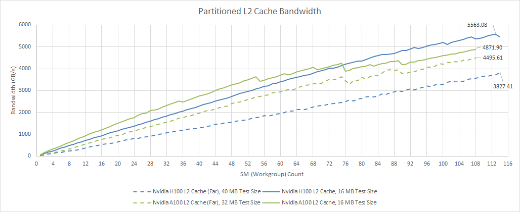
In an absolute sense, H100’s 50 MB L2 still offers a ton of bandwidth even when requests have to go across the cache’s partitions. For comparison, RDNA 2’s Infinity Cache offers around 2 TB/s of bandwidth, while RDNA 3’s Infinity Cache stops just short of 3 TB/s. H100 therefore offers a bit less caching capacity than the Infinity Cache on AMD’s top end client GPUs, but makes up for it with more bandwidth.
However, I feel like Nvidia could bring some of their client side engineering into their compute oriented GPUs. Their RTX 4090 offers about 5 TB/s of L2 bandwidth, and has a lot more L2 caching capacity. On the bright side, H100’s L2 offers much higher bandwidth than VRAM, even when requests have to cross partitions. That’s a compliment, because H100 has a ridiculous amount of VRAM bandwidth.

With five stacks of HBM2e, the H100 can pull just short of 2 TB/s from VRAM. Thus, the H100’s VRAM bandwidth is actually quite close to RDNA 2’s Infinity Cache bandwidth. It also represents a significant improvement over A100. A100 used HBM2 and still has more VRAM bandwidth than any consumer GPU, but its lower memory clocks let H100 pull ahead.
H100’s VRAM bandwidth will be very useful for massive working sets without cache-friendly access patterns. Consumer GPUs have trended towards good caching instead of massive VRAM setups. The few consumer GPUs that did use HBM have turned in a mediocre performance compared to ones with a modest GDDR setup but excellent caching. That’s because caches lower latency, making it easier to keep the execution units fed even with small workloads. From how Nvidia and AMD have been building compute GPUs, it looks like compute workloads favor the opposite. A100 was already tuned for large workloads. H100 takes that further, with a lead over A100 if you can fill more than half the GPU, but falls a bit behind if you don’t.
Compute Throughput
A100’s SMs offered higher theoretical occupancy and FP64 performance than client Ampere, but only had half the FP32 throughput. H100 remediates that by giving each SM sub partition (SMSP) 32 FP32 units, letting it execute one warp instruction per clock.
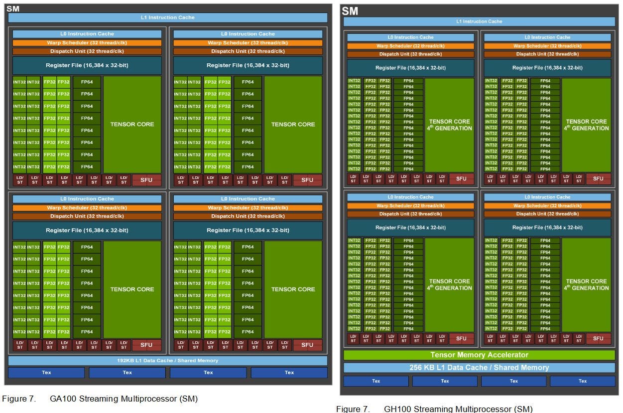
Alongside FP32 performance, FP64 performance doubles too. Each H100 SMSP can execute a FP64 warp instruction every two cycles, compared to once every four cycles on A100. That makes H100 a much better performer than A100 for scientific applications that need increased precision.

At the same time, H100 inherits Nvidia’s strength in integer multiplication. Specifically, INT32 multiplies execute at half rate, compared to quarter rate on AMD GPUs. On the other hand, AMD GPUs can execute 16-bit integer operations at double rate, while Nvidia GPUs can’t.
At the GPU level, H100 features a small SM count increase and a substantial increase in clock speeds. The result is a significant increase in compute throughput across the board. Thanks to SM-level changes, H100’s FP32 and FP64 throughput blows A100 out of the water.
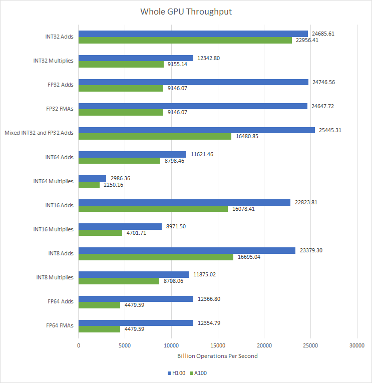
H100’s improvements should bring performance benefits across a very wide variety of applications, because it’s hard to think of any GPGPU program that doesn’t use FP32 or FP64. Doubling throughput for those operations along with a SM count and clock speed increase is going to make workloads finish faster.
Going beyond vector compute performance, H100 doubles tensor core throughput. Tensor cores specialize in doing matrix multiplication by breaking the SIMT model, and storing matrices across a warp’s registers. I don’t have a test written for tensor cores and writing one in the near future is beyond what I have time for with a free time hobby project. But, I trust Nvidia’s whitepaper on this topic.
Final Words
Consumer GPUs in recent years have moved towards maintaining good performance when faced with small workloads. They’re still very wide of course, but AMD and Nvidia have struck a balance between throughput and latency. RDNA 2/3 and Ada Lovelace run well over 2 GHz, meaning their clock speeds approach those of server CPUs. Alongside high clock speeds, sophisticated cache hierarchies provide latency benefits along with high bandwidth, provided access patterns are cache friendly. Meanwhile, expensive memory solutions have fallen out of favor. The few client GPUs with HBM never did well against their GDDR equipped competition, despite having more memory bandwidth and often more compute throughput to back that up.
But that evidently doesn’t apply to compute GPUs, because they’ve gone in the opposite direction. H100 is a massively wide GPU running at relatively low clocks, which emphasizes performance per watt over absolute performance. 1755 MHz was typical for Pascal, an architecture launched seven years ago. Cache capacity and latency are mediocre compared to recent client GPUs. Meanwhile, Nvidia has not compromised bandwidth. H100’s L2 does not fall behind client GPUs when it comes to bandwidth. After L2, VRAM bandwidth is monstrous thanks to a giant HBM configuration. H100, like A100 and AMD’s CDNA GPUs, is meant to run large, long running jobs. Based on the emphasis on VRAM bandwidth over caching capacity, these jobs probably fall into the category where if you can’t catch the access pattern with a few dozen megabytes of cache, doubling cache capacity probably won’t help.
H100 differentiates itself from client designs at the SM level too. More memory for L1 or Shared Memory use means carefully crafted programs can keep a lot of data very close to the execution units. Across H100’s 144 physical SMs, there’s 36.8 MB of L1 and Shared Memory capacity, which makes for a significant die area investment. Nvidia has also spent SM area to track more warps in flight in order to cope with higher L1 miss latency. H100 can track 64 warps per SM, compared to 48 on client Ampere’s and Ada Lovelace. Additional SM area gets spent to double FP32, FP64, and tensor throughput.
Client GPUs continue to provide reasonable compute capability, and datacenter GPUs can be forced to render graphics if you hate yourself enough. But for the foreseeable future, compute and graphics oriented architectures will likely continue to diverge. Ada Lovelace and H100 feature plenty of differences, even if they’re based off a similar base. On the AMD side, RDNA and CDNA continue to diverge too, though both can trace their ISA’s roots back to the venerable GCN architecture. This kind of divergence is natural as process node progress slows down and everyone tries to specialize to get the most out of each transistor.
If you like our articles and journalism, and you want to support us in our endeavors, then consider heading over to our Patreon or our PayPal if you want to toss a few bucks our way. If you would like to talk with the Chips and Cheese staff and the people behind the scenes, then consider joining our Discord.
Any plans to similarly benchmark blackwell? :)