AMD’s Strix Point: Zen 5 Hits Mobile
AMD’s Zen line has gone a long way since it brought AMD’s CPU efforts back from the dead. Successive Zen generations delivered steady improvements that made AMD an increasingly dangerous competitor to Intel. Zen 5 is the latest member of the Zen line, and hits the market at a point when Intel has plenty of troubles of their own.
Here, we’re analyzing the Zen 5 architecture as implemented in the Ryzen AI 9 HX 370. The HX 370 is a member of AMD’s Strix Point APUs, which combines Zen 5 cores with a RDNA 3.5 iGPU and some AI stuff. Prior Zen generations saw their mobile versions launch well after the architecture debuted in desktop products, so it’s interesting to see Zen 5 do the opposite.
Acknowledgments
We would like to thank ASUS for providing a laptop for review.
System Level
Strix Point implements 12 Zen 5 cores in a dual cluster configuration. A high performance cluster has four “regular” Zen 5 cores and 16 MB of L3 cache running at up to 5.15 GHz. A second density optimized cluster has eight Zen 5c cores and 8 MB of L3 running at up to 3.3 GHz. It’s a continuation of AMD’s mild hybrid strategy, where different cache sizes and physical implementations help the company optimize multithreaded performance while keeping area under control. It contrasts with Intel’s hybrid strategy, which uses different core architectures optimized for high performance and high density.
All cores within a cluster cap out at the same clock speed. That should simplify OS scheduling decisions, because any of the high performance cores will reach approximately 5.15 GHz.

Intel’s Meteor Lake in contrast benefits from a bit more scheduler awareness because two of its high performance Redwood Cove cores can reach 4.8 GHz. Other Redwood Cove cores cap out at 4.5 GHz. Like Strix Point, all of Meteor Lake’s efficiency cores cap out at the same speed across a cluster.
Both of Strix Point’s CPU clusters are tuned for responsiveness, and waste little time getting to their maximum clocks. Even the density optimized Zen 5c cores can reach their modest 3.3 GHz boost speed in less than two milliseconds.
Asus has opted to give the HX 370 a 128-bit LPDDR5-7500 setup, providing similar theoretical bandwidth to Meteor Lake’s LPDDR5-7467 with the same bus width. Strix Point’s CPU clusters each have 32 byte per cycle ports to the network-on-chip, which AMD calls Infinity Fabric. Infinity Fabric on the Ryzen AI 9 HX 370 runs at up to 2 GHz, much like desktop Zen 4. Per-cluster bandwidth limitations are similar. Read bandwidth from a single cluster caps out at just under 62 GB/s. The memory controller has a bit more bandwidth on tap, but you’ll need to load cores from both clusters to get it.
Unlike desktop Zen 4, Strix Point’s CPU clusters have 32 byte per cycle write links too. Per-cluster write bandwidth is therefore capped at 64 GB/s, rather than 32 GB/s on desktop Zen 4.
Meteor Lake can just about saturate the memory controller from the CPU tile, indicating its link to Intel’s Scalable Fabric has more bandwidth than Strix Point’s CCX to Infinity Fabric link. The bandwidth gap narrows if traffic is evenly mixed in both directions. Still, reading from DRAM using both clusters at the same time gets more bandwidth. These network-on-chip bandwidth limits are unlikely to be a factor, as low-threaded applications tend to need less bandwidth. Meteor Lake’s design also demands more bandwidth from its cross-die link because the bulk of its CPU performance is concentrated on the CPU tile.
Cache coherency operations like lock cmpxchg see higher than expected latency when crossing cluster boundaries. This core to core latency measurement usually returns numbers under 100 ns for desktop CPUs, even when crossing die boundaries. The Ryzen AI 9 HX 370 uses a monolithic setup, so higher latency here is a bit surprising.
For comparison, the Ryzen 9 3950X keeps cross-cluster latencies in the 80-90 ns range. Both setups enjoy excellent core to core latency within a cluster.
Zen 5 Core, High Level
Zen 5 is a significant evolution of the Zen line. From the cpuid instruction, Zen 5’s family is 1A in hexidecimal. To use AMD’s typical terminology, Zen 5 is a member of the 1Ah family (h stands for hexidecimal). Zen 3 and Zen 4 were identified as 19h, while Zen 1 and Zen 2 were 17h.
The CPU family reported by cpuid isn’t always significant. Intel for example identifies everything from the original Pentium Pro to Golden Cove as belonging to the 6h family. In AMD’s case though, Zen 5 sees substantial changes over Zen 4. Giving Zen 5 a different family designation definitely seems appropriate.
While Zen 5 inherits characteristics from Zen 4, just about every part of the CPU’s execution pipeline has changed substantially. The branch predictor is more capable and gets a victim-cache BTB setup. The fetch and decode stages are arranged in two clusters. The out-of-order backend shifts towards unified schedulers on the integer side while doing the opposite for floating point. Memory accesses benefit from larger TLBs and a bigger L1. And of course, Zen 5 is wider and has more reordering capacity than its predecessor.
Branch Prediction
AMD had an excellent predictor since Zen 2, and that predictor has gotten even better over time. Zen 5 continues the trend, building on top of Zen 4’s already class leading predictor. AMD needs an accurate branch predictor to make the most of a wider core with more reordering capacity, and Zen 5 doesn’t disappoint. It can recognize extremely long patterns, and is a solid step above Zen 4. Zen 4 is itself a good step above Intel’s current P-Cores.
Branch predictors have to be fast in addition to being accurate, because the whole point of branch prediction is to mitigate frontend stalls caused by branches. A cache of frequently used branch targets (called a BTB, or Branch Target Buffer) helps with speed, and is especially useful if instruction bytes have to be fetched from higher latency L2 or L3 caches.
Zen 5 moves into the company of cores like Golden Cove with giant BTBs. AMD’s latest BTB arrangement is unique because the last level has fewer entries than faster levels. I can’t think of any other CPUs that use such a BTB setup, but it makes sense in the same way having less L3 per core than L2 is fine. BTBs are caches after all, just for branch targets instead of data. AMD and others have used L3 victim caches for data in many CPUs. Now, AMD’s branch target caching works the same way. Targets evicted from the 16384 entry L1 BTB to make room for incoming targets are filled into the L2 BTB in case they have to be used again soon. The net effect is Zen 5 can track 24K branch targets, and sometimes more.
Each BTB entry can hold up to two branches if the branches reside in the same 64-byte aligned cache line and the first branch is a conditional branch
Software Optimization Guide for AMD Family 17h Models 30h and Greater Processors
Optimization manuals for prior Zen generations indicated that a single BTB entry could store targets for two branches provided certain conditions were met. Perhaps we’re seeing that capability apply more broadly with Zen 5.
Besides high branch target caching capacity, Zen 5’s predictor deserves recognition for how fast it can go. The first BTB level can track up to 1024 branches and handle two taken branches per cycle. AMD is not the first to release a core capable of sustaining two taken branches per cycle. Intel did that with Rocket Lake, and Arm did the same with Cortex X2. But Zen 5 joins that party in style, achieving that speed across a much larger branch footprint than either Neoverse V2 or Golden Cove. As a cherry on top, Zen 5 does that while clocking above 5 GHz in a mobile form factor.
Returns are predicted by a 52 entry return stack, which appears to be duplicated for both SMT threads. It’s substantially larger than the 32 entry return stack in prior Zen generations.
Clustered Fetch and Decode
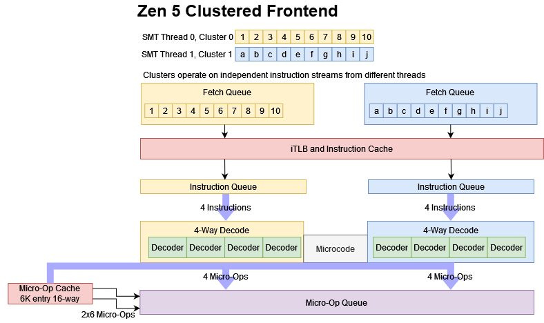
After the branch predictor decides where to go, subsequent frontend stages fetch instructions from memory and decode them into the CPU’s internal format. Zen 5 arranges these fetch and decode stages into two clusters. Each cluster can fetch 32 bytes per cycle from the 32 KB instruction cache and decode up to four instructions per cycle. Together, the decode clusters can handle eight instructions per cycle.
Superficially, Zen 5’s frontend looks like the ones in Intel’s latest E-Cores. However, they don’t work the same way. Each Zen 5 cluster only handles a single thread, and maximum frontend throughput can only be achieved if both SMT threads are loaded. Intel’s scheme has all clusters working in parallel on different parts of a single thread’s instruction stream. Mixing taken branches into the test for Zen 5 doesn’t improve throughput as it did with Intel’s first generation clustered decode implementation in Tremont. Therefore, Zen 5 is likely not using branches to load balance between the two decode clusters.
To further speed up instruction delivery, Zen 5 fills decoded micro-ops into a 6K entry, 16-way set associative micro-op cache. This micro-op cache can service two 6-wide fetches per cycle. Evidently both 6-wide fetch pipes can be used for a single thread.
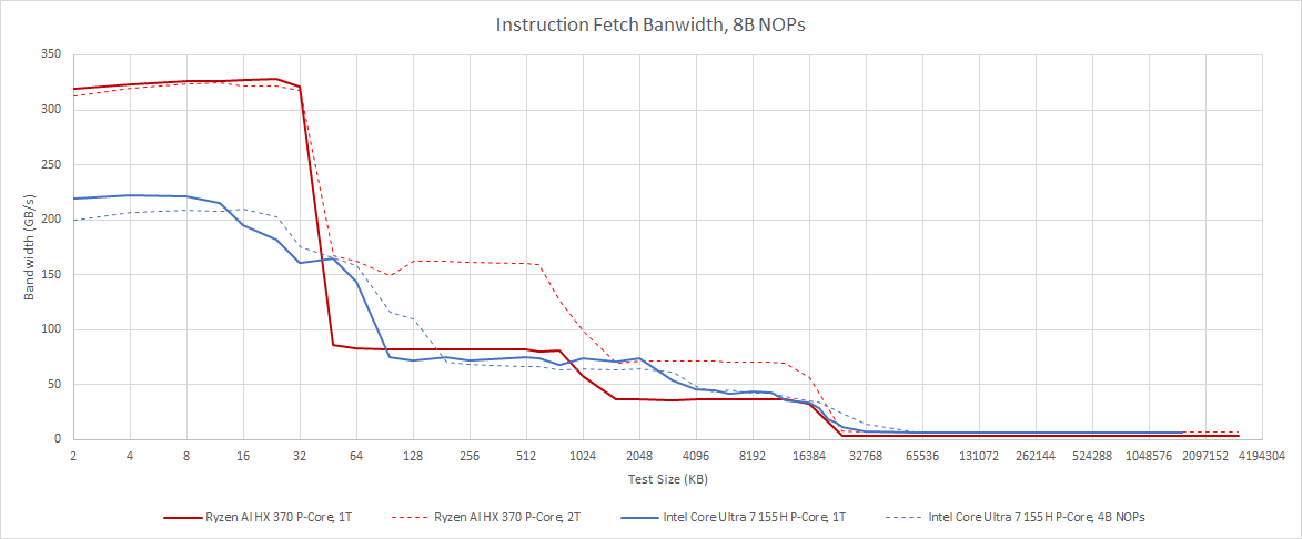
Zen 5 can sustain higher instruction throughput than Intel Meteor Lake’s Redwood Cove P-Cores, but only for small instruction footprints or when both SMT threads are loaded. If only a single SMT thread is active, Intel’s larger 64 KB instruction cache and conventional 6-wide decoder can hand it a lead when code spills out of the micro-op cache.
Because x86 is a variable length instruction set, instruction cache bandwidth can become a limiting factor before the decoders do. Zen 5 and Golden Cove are practically immune to instruction length issues when they hit their respective micro-op caches. AMD’s slides suggest the L1 instruction cache can provide 64 bytes per cycle, but I was only able to get half that even with both SMT threads loaded. If code spills out of L2, Zen 5 can still maintain respectable frontend bandwidth. However, bandwidth is definitely better if you can use both SMT threads, suggesting there’s a limit to how many L1i fill request Zen 5 can queue up for a single thread.
Rename and Allocate
Operations from the frontend need backend resources to track them and enable correct out-of-order execution. Zen 5’s renamer is 8-wide, making it 33% wider than Zen 4’s 6-wide renamer. With every other stage in the core at least as wide, that means Zen 5 is an 8-wide core. The renamer is also a good place for tricks like move elimination or zeroing idiom recognition. Both can expose more parallelism to the backend, and even avoid consuming backend resources like register file entries. Like prior Zen generations, Zen 5 does plenty of this.
Zen 5 can generally pull these optimizations off at 8 per cycle, but not for a single thread. It would be rare for code to zero so many registers or move a lot of values between registers in close proximity, so those renamer restrictions may have let AMD simplify this stage. Two SMT threads will of course have independent instructions, and Zen 5 maintains the ability to blast through that quickly should both threads happen to hit a sequence of zeroing idioms or register-to-register MOVs at the same time.
Giant Backend, Unified Schedulers
CPUs use various structures in the backend to let them execute instructions as data becomes available for them while ensuring results are consistent with in-order execution. AMD’s Zen line was often light on these resources compared to contemporary Intel cores, and couldn’t look as far ahead in the instruction stream to hide latency. A lower latency cache hierarchy helped keep AMD’s performance competitive.
Zen 5 continues to have smaller structures compared to Intel, but significantly closes that gap in some areas. Its reorder buffer, FP register file, and load queue sizes are quite close to Golden Cove’s. The integer register file sees less of a size increase, possibly because it’s hard to feed 6 ALU and 4 AGU ports while adding a ton of register file entries. And while AMD’s store queue has grown substantially, entries are still 256 bits. 512-bit stores will take two entries just as with Zen 4.
AMD also made compromises with the FP/vector register file. Testing shows about 234 entries are available for in-flight instructions that write to 512-bit ZMM registers. Zen 5 is not allocating pairs of 256-bit registers to handle a 512-bit operation. AMD’s slides clearly indicate the vector register file has 384 entries, but 234 * 2 would be 468 physical 256-bit registers. Mixing a ZMM write reduces reordering capacity for 256-bit YMM registers by exactly one, implying only a single register was allocated to hold that 512-bit result. However, testing by Mystical shows that all vector register file entries on desktop Zen 5 are 512-bits wide.

Zen 5’s rename/allocate stage sometimes handles register allocation poorly. Alternating between writing to ZMM and YMM registers should not reduce reordering capacity for FP/vector results, because more than half of Zen 5’s register file entries are 512 bits wide. Intel’s Golden Cove does exactly that, but Zen 5 stops at 288 registers (144 of each). That’s still more register file capacity allocated than what a hypothetical fully 256-bit register file would have, but it does point to less than optimal allocation.
With Zen 4, AMD used a fully 512-bit vector register file because using wider entries only had a minor area hit compared to increasing register file port count or width. A 512-bit register file with twice as many entries as Zen 4’s might have been impractical for a mobile core. Splitting vector registers into two pools feels like a good compromise, especially considering Zen 5 still has more 512-bit register file entries than Zen 4 had in total.
FP/Vector Execution
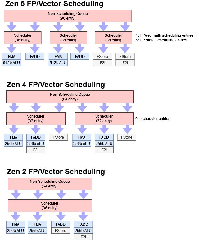
Across Zen generations, AMD has slowly moved towards a more distributed FP scheduler layout. AMD is adding new scheduling queues while cutting down on port count per queue, but without significantly changing entry count. In Zen tradition, the rename/allocate stage can dump FP/vector ops into a huge non-scheduling queue if the schedulers are full rather than stalling. This queue is even larger now, with 96 entries instead of 64 as in prior generations. 64 entries was already a lot, and Zen 2 would often run out of FP register file entries before filling the schedulers and non-scheduling queue. Zen 5’s giant register file should make things more balanced.
Zen 5’s floating point execution unit layout is immediately recognizable as something from the Zen family. FP math operations use four ports, two of which do floating point multiplies and fused multiply adds (FMAs). The other two handle floating point adds. FP adds and multiplies have 3 cycle latency, while FMAs have 4 cycle latency. All of the FP math units are 256-bits wide, as with Zen 2. AMD is focused on feeding its existing execution units rather than having bigger ones.
Vector integer execution sees changes that are probably geared towards keeping power and area under control. Vector integer addition latency goes up to two cycles, compared to one cycle on Zen 4. Execution rate for 128-bit SSE and 256-bit AVX2 packed integer adds has gone from four per cycle down to two per cycle. Vector integer throughput is still the same at 1024 bits per cycle, but programs will need to use AVX-512 to get there. Having fewer, wider vector integer ports may cut down on power because fewer operations are sent from the schedulers and fewer distinct register file reads happen for the same number of compute operations. But prior Zen generations are just a bit more nimble in that regard.
Integer Execution
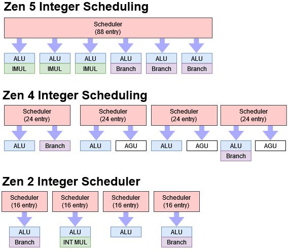
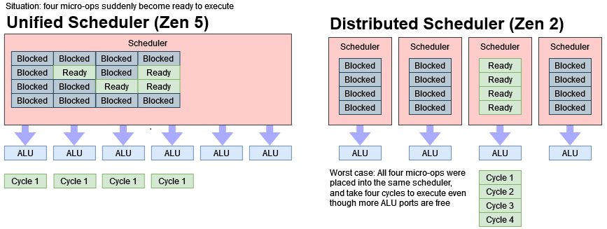
Scalar integer execution goes in the opposite direction. Zen 5 has one big unified 88 entry scheduler, capable of selecting six operations per cycle to feed the core’s six integer execution ports. It reminds me of big unified schedulers from Intel’s Core line. Meteor Lake’s Redwood Cove uses a 96 entry scheduler to feed six integer execution ports. Zen 5 uses separate ports and schedulers for its vector/FP units, but the size and port count of both schedulers is quite similar.
Prior Zen generations and Intel’s E-Core line use a more distributed scheduling scheme. Using separate schedulers means each scheduler doesn’t have to select as many operations per cycle. But that often makes schedulers more specific to certain operations, which increases the risk of filling up one scheduling queue and causing the renamer to stall, even if scheduling entries are available in other queues.
Using a unified scheduler also makes it possible to assign operations to execution ports right before they’re issued to those execution units, rather than at the renamer. That can provide additional flexibility, avoiding corner cases where several ops in one scheduler become ready, but all of them experience contention for that scheduler’s port. A unified scheduler doesn’t necessarily mean port selection happens right as micro-ops become ready, but AMD did talk about that in an interview so Zen 5 likely does this.
Address Generation
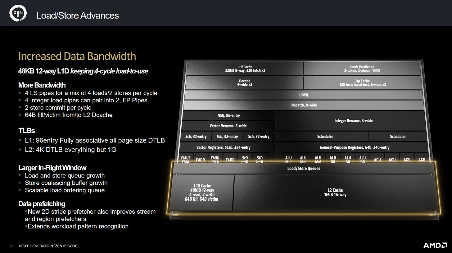
Memory operations get their addresses generated by four address generation units (AGUs), which are fed by a unified 58 entry scheduler. Zen 4 could technically give more scheduler capacity to memory operations, but those entries had to be shared by integer math operations.
Zen 5 is therefore a bit like Zen 2, with a unified AGU scheduler separate from the integer units. Of course, Zen 5’s AGU scheduler has about twice as much capacity as Zen 2’s, and feeds four ports instead of three. The four AGUs let Zen 5 sustain four scalar integer memory accesses per cycle. All four can be loads, and up to two can be stores.
Memory Dependencies and Alignment
After calculating addresses, the load/store unit has to ensure memory operations appear to execute in the correct order. If a program loads data from a memory address that it wrote to soon before, the load might have to get its data from an in-flight store rather than the cache hierarchy. Like prior Zen CPUs, Zen 5 can do fast store forwarding as long as the load is contained within the prior store. The most common and trivial case of an exact address match is handled with zero latency, carrying forward a feature introduced with Zen 3. Because Zen 5 has four AGUs, it can do zero latency forwarding for two dependent load-store pairs. Zen 3 and Zen 4 could only do so for one pair at a time. Intel’s Golden Cove has similar behavior for the exact address match case, but can’t do zero latency forwarding if both the load and store cross a 64B boundary.

Cases where the load is contained within the store are handled with 7 cycle latency. Zen 4 was a bit faster because it could occasionally do that with 6 cycle latency. Intel’s Golden Cove could do that with 5 cycle latency, but fares worse if fast store forwarding fails due to a partial overlap. Golden Cove suffers a 19-20 cycle penalty in that case, higher than Zen 4’s 18 cycle penalty and much higher than Zen 5’s 14 cycle penalty.
Looking at independent loads and stores shows that Zen 5’s data cache has 64 byte alignment for both loads and stores. That reduces throughput losses from misaligned stores. AMD used 32 byte store alignment for Zen 2 through Zen 4, and 16 byte store alignment on Zen 1. All Zen generations have 64 byte load alignment.
The penalty for a misaligned store has gone down too, with Zen 5 able to handle a misaligned store every cycle. Maybe Zen 5’s data cache has two write ports.
Address Translation
Programs use virtual addresses, which have to be translated on-the-fly to addresses in physical memory. CPUs speed this up by caching recently used translations in TLBs, or translation lookaside buffers. Zen 5 increases TLB sizes to reduce address translation delays.
AMD uses separate TLB hierarchies for instruction and data. Zen 5’s instruction side sees its L2 TLB quadruple in size, while the data side gets 33% TLB capacity increases on both levels.
Getting a translation from Zen 5’s L2 DTLB costs 7 extra cycles, the same as on Zen 4. AMD has therefore managed a substantial L2 TLB size increase with no latency penalty. Intel has a smaller L2 TLB, which is also shared with instruction accesses. Redwood Cove’s L2 TLB latency is also 7 cycles. Intel’s caching capacity for address translations comes up short compared to AMD’s, which can increase memory access latency seen by software.
Cache and Memory Access
Good caching is vital to performance. Zen 5 uses a familiar triple level cache hierarchy, but AMD has made the L1 data cache bigger. Even though the L1D grows from 32 to 48 KB, latency remains at 4 cycles. Load bandwidth for Strix Point remains the same at 64 bytes per cycle as Zen 4, but the store bandwidth has increased to 64 bytes per cycle so that Strix can deal with 1 512b store per cycle. AMD has thus increased per-cycle L1D bandwidth for the first time since Zen 2.
Bandwidth increases continue to Zen 5’s L2 cache, which has 64 byte per cycle read and write paths. Exercising both paths with a read-modify-write pattern achieves about 85 bytes per cycle with L2-sized arrays. While not quite 128 bytes per cycle, it’s comfortably above the 64 bytes per cycle that Zen 4 is limited to.
From L3, a single core can achieve 32 bytes per cycle with only reads or only writes, or 64 bytes per cycle with an even mix of both. L3 bandwidth in this case is capped by the core’s 32 byte per cycle interface to the intra-CCX interconnect. It’s a bit better than Zen 4, which couldn’t quite hit 32 bytes per cycle from L3 with a single core active.
With all cores in play, Zen 5’s mild hybrid setup gives it a cache bandwidth edge over Intel’s Meteor Lake. Even though Meteor Lake has 16 cores to Strix Point’s 12, all eight of Strix Point’s area optimized cores use the same architecture as their high performance counterparts and have the same 64 bytes per cycle of load bandwidth. Meteor Lake’s Crestmont efficiency cores can only load 32 bytes per cycle from their data caches. The gap widens at lower cache levels, where Intel has four E-Cores share a L2 instance with 64 bytes per cycle of bandwidth.
DRAM bandwidth is similar, with Intel’s Core Ultra 7 155H getting 83 GB/s to Strix Point’s 79.9 GB/s. It’s not a big difference, and both chips enjoy plenty of bandwidth from their LPDDR5 setups.
Latency
Zen 5’s cache latency characteristics don’t change much compared to Zen 4, which is great because Zen 4 generally does well in that regard. The Zen 5 cluster takes 2-3 extra cycles to access its larger 16 MB L3 cache, but it’s a very minor difference and well worth the extra capacity the cache provides. AMD’s work on the L2 is appreciated too, as they’ve managed to keep latency at 14 cycles despite increasing associativity from 8-way to 16-way.
Actual latency is of course much better on the high performance Zen 5 cluster thanks to higher clock speeds. Against Intel’s Redwood Cove, Zen 5 enjoys better latency at every level in the memory hierarchy. Sometimes though, Intel can have an advantage because Meteor Lake gives its P-Cores access to more cache capacity. Intel’s L2 is larger of course, at 2 MB versus 1 MB on AMD. And Meteor Lake can give one core access to 24 MB of L3 capacity while Strix Point splits its 24 MB of L3 into separate instances.
DRAM latency is around 128 ns on the Ryzen AI 9 HX 370. It’s better than Intel’s Core Ultra 7 155H, which sees 148 ns of memory latency. Even though both chips use a similar LPDDR5 configuration at first glance and achieve similar bandwidth figures, AMD somehow gets better latency. However, even AMD’s LPDDR5 controller suffers much higher latency than DDR5. The 7950X3D with DDR5-5600 for example has well under 100 ns of DRAM latency.
Some Light Benchmarking
Detailed performance benchmarking is best left to mainstream tech outlets, which have more time and resources. Still, it’s interesting to look at how Zen 5 stacks up against Intel’s current Meteor Lake architecture. I’m testing Meteor Lake in my Asus Zenbook 14 OLED. I’ve also run the video encoding test on my Ryzen 7950X3D desktop, locked to the non-VCache die and with clock speeds capped to 5.15 GHz.
Even with the same core count and maximum clock frequency, desktop Zen 4 comfortably pulls ahead of mobile Zen 5. In a desktop platform, a Zen 4 core has access to twice as much L3 cache and lower latency DDR5. That goes to show how important the memory subsystem is. Against Intel, Strix Point comfortably smashes Meteor Lake in a matched core count test.
AMD’s AVX-512 support is a factor in this test. Without AVX-512 support, Intel has to execute about 10% more instructions to complete the workload. Intel can’t clock as high as AMD can either. Therefore, Redwood Cove falls behind even though it’s averaging more instructions per cycle. Seeing AMD take the lead with AVX-512 being a factor is weird. Intel released the first AVX-512 capable CPUs on the market, and AMD’s AVX-512 implementation still feels conservative.
AMD has invested a lot of core area into their branch predictor since Zen 2, and it has paid off in the past. Zen 5 keeps pushing on that area, but might be running into diminishing returns.
Zen 5’s branch predictor may be more accurate, but in this workload the difference is so small it’s within margin of error. More capable branch predictors run into diminishing returns.
Final Words
Zen 5 makes sweeping changes throughout the pipeline. The core gets wider, boasts more reordering capacity, and improves caching capacity within the core without taking a latency hit. That’s not just for data. Zen 5 can cache more address translations in its TLBs, and more branch targets in its BTBs. Latency has even gone down in some cases. Being able to deal with 1024 branches in flight with effectively 0.5 cycle latency is an impressive achievement. A lower penalty for failed store forwarding suggests AMD was able to cut down pipeline length between address calculation and store retirement, since that’s a straightforward way to fall back when fast store forwarding fails.
Considering other significant changes like a clustered frontend, different scheduler layout, more execution units, and extra cache bandwidth makes me feel like Zen 5 involved a lot of engineering effort. It’s a refreshing contrast compared to Intel Meteor Lake’s Redwood Cove and Crestmont, which made very minor changes over Raptor Lake and Alder Lake’s respective P and E cores.
Another contrast with Intel is AMD’s focus on SMT. Intel has indicated a shift away from SMT, at least for mobile products like their upcoming Lunar Lake. Implementing SMT by itself doesn’t cost a lot of area or power. But optimizing a core for SMT can involve increasing core structure sizes to ensure each thread gets a healthy amount of entries when two SMT threads are active. Intel decided their hybrid strategy could deliver high multithreaded performance without having to chase diminishing returns further than they wanted to for a single thread.
AMD takes the opposite approach. Zen 5 seems to be designed with a strong focus on SMT. Certain parts of the core like the renamer and decoders need two threads active to achieve their full potential. AMD still emphasizes single threaded performance of course, but they’re chasing multithreaded performance with a combination of density optimized physical implementations and SMT, rather than different core architectures. That strategy does come with some advantages, like keeping AVX-512 enabled across the company’s CPU lineup. Maybe AMD is wise to twist the knife while Intel inexplicably refuses to add AVX-512 support to its E-Core line.
These contrasting approaches show there’s often no clear right or wrong choice when it comes to CPU architecture. Intel and AMD both have a lot of smart engineers. Both have gone in different directions when choosing between unified and distributed schedulers, whether to prioritize SMT, or how to create a hybrid core setup. Those decisions change even within the same company. AMD went from a 256-bit vector register file, to a fully 512-bit one, and then to a lopsided one with both 256-bit and 512-bit entries. Another choice is how to balance performance per clock gains against clock speed. Zen 5 de-prioritizes the latter, since Strix Point barely clocks higher than Phoenix.
Therefore Zen 5’s performance gains are lower compared to prior Zen generations due to a lack of an increase in clock speed, even though the headline IPC gain is in-line with what those prior generations offered. Hopefully Zen 5 sets a solid foundation for AMD to build future CPUs off.
Again, we would like to thank ASUS for sending us over a ProArt PX13 for review and if you like our articles and journalism, and you want to support us in our endeavors, then consider heading over to our Patreon or our PayPal if you want to toss a few bucks our way. If you would like to talk with the Chips and Cheese staff and the people behind the scenes, then consider joining our Discord.










Hi Chester,
I'm a student from China and I plan to make some analysis in AMD's Strix Point. I have read your analysis in intel Meteor Lake and learn a lot. Do you have some advices in how to make the analysis in Strix Point's NPU?
Best Regards
Charles