
Sunny Cove: Intel’s Lost Generation

This is going the be the first in a series of articles on CPU architectures. We’re picking up where Real World Tech left off with its microarchitecture deep dives. And we’re going to be doing them with the advantage of 20-20 hindsight, and hardware to test on.
Sunny Cove is technically the successor to Intel’s well known Skylake architecture. The word ‘technically’ applies because Sunny Cove never fully replaced Skylake throughout Intel’s product stack, before itself getting replaced by Golden Cove. Despite being announced in Intel’s 2018 Architecture Day, persistent 10nm process struggles meant Sunny Cove only appeared in the consumer market in late 2019, in ultra-low power form. Intel took until late 2020 to push Sunny Cove into larger laptops.
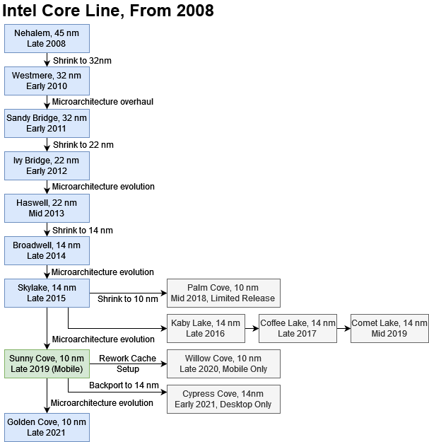
In desktops, Intel’s top of the line CPUs remained Skylake based until early 2021, when Sunny Cove finally took over in Rocket Lake form. Rocket Lake used the Sunny Cove core backported to Intel’s mature 14nm process. The older, more mature process let it hit the high clocks required to be competitive on desktop, but at tremendous power cost. Rocket Lake failed to match Zen 3, and often even failed to outshine Skylake in gaming. In less than a year, Alder Lake launched, ending Sunny Cove’s role as Intel’s flagship architecture without giving it a serious chance to prove itself.
Yet Sunny Cove tells us a lot about Intel’s post-Skylake efforts. It puts to bed the idea that Intel was complacent and resting on their laurels because AMD was uncompetitive. The architectural changes from Skylake to Sunny Cove are downright ambitious, and represent one of Intel’s biggest microarchitecture changes since Sandy Bridge. And because a new CPU architecture takes several years to finalize, work on Sunny Cove likely started before Zen 1 released in 2017.
Overview and Block Diagram
From a mile up, Sunny Cove is a high performance core with very deep out of order execution capabilities. But what sets it apart is how much different it is from its predecessor. Unlike the move from Haswell to Skylake, Intel has made changes in nearly every part of the pipeline to make Sunny Cove. Notably, Sunny Cove is 5-wide at its narrowest point, making it the first time Intel has increased core width in over a decade.
Skylake is a much smaller core. It’s still high performance, with high clock targets and very good ILP-extraction capability.
Frontend: Branch Prediction
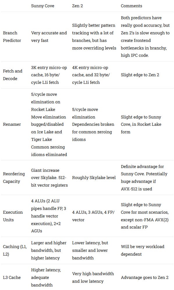
Branch prediction’s importance can’t be understated. The branch predictor is responsible for steering the CPU core, letting it avoid stalling every time a control flow instruction shows up. Of course, how often it can avoid penalties from branches depends heavily on the branch predictor’s ability to remember branch targets (and how fast it can retrieve them), and how accurately it can predict branch direction.

Intel has made moves in both areas. Sunny Cove’s branch predictor can recognize much longer patterns than Skylake’s. When there are a lot of branches, Sunny Cove is better at tracking their histories without aliasing issues. That hints at much larger branch history tracking structures at play behind the scenes.
Compared to AMD’s Zen 2, Sunny Cove can track patterns that are about as long, but does worse when there are a lot of branches in play. Zen 2’s predictor probably has more storage for branch history, but it isn’t any better when it comes to dealing with a few branches that require long history tracking to predict. In fact, it’s slower when dealing with more “difficult” branches, because it’s using a multi-level predictor. Zen 2 seems to use a fast predictor with limited pattern recognition capability, followed by a higher latency but more accurate predictor that can override the first one. Sunny Cove doesn’t suffer any such penalties, suggesting it packs all of its branch direction prediction logic into a single fast predictor.

For tracking branch targets, Sunny Cove features a larger main BTB than Skylake while staying at 2 cycle latency. 4K to 5K isn’t a huge change, but it’s Intel’s first BTB capacity increase since Sandy Bridge went to 4K entries, up from 2K entries in Westmere. Sunny Cove doesn’t stop there, and introduces speed improvements too. It can handle 256 taken branches with no pipeline bubbles – double what Skylake (and Haswell) could do. And Intel has some cool tricks up its sleeve. Sunny Cove can unroll loops within its micro-op queue, essentially turning it into a tiny trace cache. That lets it complete up to two taken branches per cycle within small loops.
Against AMD’s Zen 2, Intel enjoys a huge speed advantage with taken branches. Skylake already puts in a very good performance compared to Zen 2, and Sunny Cove increases Intel’s lead. Zen 2 can only track 16 branch targets without penalty. In practice, that’s only enough to handle about 50% of branches. With thousands of branches in play, Zen 2’s taken branch throughput drops to one per 5 cycles, while Intel still maintains decent throughput at one branch per two cycles.
Frontend: Fetch and Decode
Sunny Cove’s frontend sees substantial changes as well. For the first time since Sandy Bridge, Intel has increased micro-op cache capacity, from 1.5K entries to 2.3K. Compared to Skylake, we can clearly see the bigger micro-op cache with an instruction bandwidth test:
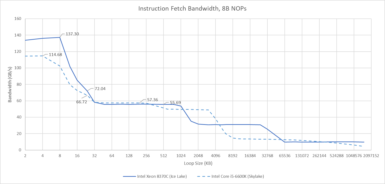
If we divide by clock speed to show bytes per cycle, we can see how the micro-op cache increases instruction bandwidth beyond what the L1 instruction cache can provide. Sunny Cove enjoys a big instruction bandwidth advantage over Skylake in the micro-op cache region, but we’re not really looking at frontend bandwidth there. Throughput on both CPUs is restricted by the rename stage after it, and Sunny Cove’s is wider. Still, one interesting observation is that Sunny Cove has an effective micro-op cache bandwidth of over 32 x86 instruction bytes per cycle.

Like Skylake, Sunny Cove has very robust instruction prefetching that can hide L2 latency. Instruction throughput with 4B NOPs remains close to 4 IPC as long as test sizes stay within L2. Sunny Cove does take a sharper drop in L3, but that’s because it was tested on an Ice Lake server configuration. Compared to a small ring, mesh based L3 caches tend to perform very poorly in terms of bandwidth and latency. Sunny Cove’s lower instruction fetch bandwidth from L3 is simply a reflection of that.

Compared to Zen 2, Sunny Cove still has a smaller micro-op cache. AMD also benefits from a very fast L3, potentially giving it an instruction bandwidth advantage when dealing with very large code footprints.
Rename and Allocate: Matching AMD’s Advances
Intel has increased the renamer’s width from 4-wide in Skylake to 5-wide in Sunny Cove. As noted before, this is the first increase in core width since Merom took Intel from 3-wide to 4-wide in 2006. Skylake did increase the frontend width to 6-wide by increasing micro-op cache fetch bandwidth, but the whole pipeline remains 4-wide because the renamer can only handle 4 micro-ops per cycle. Sunny Cove changes that.
Sunny Cove’s renamer also enjoys advantages beyond a simple width increase. Its move elimination capabilities have been greatly expanded, and Sunny Cove can eliminate a chain of dependent register to register MOVs at up to 5 per cycle. Intel had some move elimination capabilities starting with Ivy Bridge. But move elimination would often fail if confronted with too many elimination candidates. This is addressed with Sunny Cove, and brings Intel’s move elimination capabilities up to par with AMD’s.

Sunny Cove can also recognize special cases of independence, like zeroing a register by XOR-ing it with itself. Of the cases we tested, SUB r,r and XOR r,r are both eliminated. They execute at 5 per cycle, even though Sunny Cove only has four ALU pipes. Interestingly, MOV r, 0 is recognized as independent, but not eliminated. Throughput for that instruction is still restricted by ALU port count.
Sunny Cove’s Much Beefier Out of Order Execution Engine
The point of large out-of-order buffers is simple – they let the CPU track instructions ahead of a stalled one, and hopefully keep the execution units busy instead of simply getting stuck on one long latency instruction. But allocating these resources is much more complicated, and some structures are more expensive than others.
In just about every area, Sunny Cove has beefed up structure sizes compared to its predecessor. This is no surprise – makers of high performance CPUs regularly do this between generations. But the magnitude of Sunny Cove’s structure size changes set it apart.

Sunny Cove makes huge structure size increases almost across the board, especially in key structures like the ROB, register files, and scheduler. Size increases beyond 50% are not uncommon. Skylake’s improvements over Haswell look small in comparison. Going back over previous generations, we can see how much Sunny Cove stands out:

ROB size provides a rather rough estimate of a core’s out of order execution window size, because reordering capacity is often limited by other structures. Still, it’s a good demonstration of just how much bigger Sunny Cove is relative to its predecessors, because other resources typically increase in proportion to ROB size increases. Sunny Cove mostly does that. The integer register file, scheduler, branch order buffer, and load queue all get proportional (or better) size boosts. The store queue and FP register files get smaller size increases, but entry count doesn’t tell the whole story. Both of those structures have to deal with 512-bit data width in Sunny Cove, and can indirectly give a large uptick in reordering capability by reducing the number of operations needed to do something.
Scheduling and Execution
A large, unified scheduler has been a defining characteristic of Intel’s P6 line. After Sandy Bridge, it’s one of the few remaining places where you could draw a line back to P6. But increasing port count on a large unified structure is probably quite expensive. Starting at least with Haswell, Intel has been slowly moving away from that by not letting memory ops utilize the entire scheduler. Skylake splits the scheduler, with address generation and math using operations using separate scheduling queues.

With Sunny Cove, Intel continues the trend and uses an even more distributed scheduler. That allows even more execution ports, and an increase in total scheduler entry count by 65%. Sunny Cove’s memory execution side sees the biggest changes. Loads and stores each get a pair of dedicated AGUs, ditching the 2x general purpose AGU setup used since Sandy Bridge.

This new AGU layout makes memory scheduling simpler. It avoids the scheduling problem in Haswell and Skylake where peak L1D bandwidth couldn’t be sustained if store instructions got bound to one of the general purpose AGUs. And, it improves Sunny Cove’s L1D bandwidth for memory copies.
A Lost AVX-512 Opportunity
Skylake introduced AVX-512, but only on server variants. That’s likely because its huge AVX-512 units were too power and area hungry to make sense on client designs, especially when the same core had to serve in ultrabooks. Sunny Cove brings AVX-512 support down the stack by using a cut-down AVX-512 implementation in client designs. It doesn’t sport the giant 2×512-bit FPU setup found in server chips. But it still has a very capable AVX-512 implementation, with 2×512-bit execution for integer operations.
If Sunny Cove’s rollout had been more successful, it would have increased AVX-512 market penetration. Relatively cheap Sunny Cove client devices could be used as development platforms for AVX-512. And if AVX-512 found its way into more software, Intel could soften the blow of AMD’s core count advantage.
Memory Execution
Besides the beefed up address generation setup, Sunny Cove’s load/store unit has been tweaked to handle store forwarding more efficiently. Previous generations (since Sandy Bridge) seem to do a coarse comparison at 4 byte granularity, followed by a slower but more complete check if a load and store both touch the same 4 byte aligned block. This adds latency to non-overlapping loads and stores that are too close together, and gives the store forwarding latency plot a sort of jagged edge:
Sunny Cove gets rid of the two-level check while keeping latency the same for successful store forwarding, hinting at more complex logic in the load/store unit. At the same time, Sunny Cove suffers from higher penalties if a load and store partially overlap.

Compared to AMD’s Zen 2, Intel’s store forwarding is on roughly similar territory. However, AMD’s data cache natively operates on 32-byte (256-bit) blocks, making it slightly more prone to suffering from misaligned accesses.

Memory Access and Caching
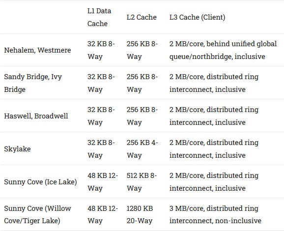
Sunny Cove shakes up Intel’s cache hierarchy for the first time in over a decade. Since Nehalem, Intel has used 32 KB L1 caches, and a fast 256 KB L2 mid-level cache to insulate the cores from a slower but much larger L3. Sunny Cove makes both caches bigger, and uses two L2 configurations within the same core architecture generation. Technically Skylake did this as well, but Sunny Cove is the first to have two L2 configurations within client parts.
These variants complicate cache hierarchy comparisons. If we started plotting everything we wanted to on the same graph, it’d be an unintelligible mess of lines. Let’s start by comparing two of Sunny Cove’s latest variations against Comet Lake, the last iteration of Skylake, and see how Intel chose to evolve their cache hierarchy.

Starting at the L1D, Intel opted for a 50% larger cache at the expense of an additional cycle of latency. Skylake doesn’t have an all-around speed advantage though, because it only achieves 4 cycle L1D latency for instructions that use “simple addressing”. “Simple addressing” means the instruction specifies a memory address base and an offset less than 2048. If the instruction asks for a more involved address calculation, Skylake’s L1D latency goes up to 5 cycles.

In 7-Zip, most memory operations only used a base and a 8-bit offset, or no offset. Approximately 23% of memory operations however used indexed addressing, or a 32-bit offset. Skylake still has an overall advantage in L1D latency, but it’s not as simple as four cycles versus five.
Moving on to the L2 – Rocket Lake (and presumably early “Ice Lake” mobile parts) double L2 size compared to Skylake at minimal cost. Bringing size to 512 KB was basically free for Intel, if we consider that hitting the L2 on both Skylake and Rocket Lake adds an extra 8 cycles over a L1 hit. Tiger Lake takes a different strategy. L2 size increases to 1280 KB, at the expense of L2 latency going to 14 cycles. One extra cycle might not seem like a massive difference. But on Intel’s problematic 10nm process, Tiger Lake struggles to hit the same clocks that Rocket Lake and Skylake reach on the more mature 14nm process. L2 load to use latency is therefore around 22.3% higher on Tiger Lake.

Rocket Lake sports an evolution of Intel’s ring-based L3, first introduced with Sandy Bridge. Like previous implementations of this design, Rocket Lake’s L3 enjoys reasonably good latency characteristics.
Tiger Lake increases L3 slice size to 3 MB, increasing total L3 size to 24 MB. At the same time, the L3 has been changed to not be inclusive of the L2. With 10 MB of total L2, an inclusive L3 would use over 40 percent of its capacity duplicating L2 contents to maintain cache coherency. Changing to a non-inclusive policy dictates changes to the L3’s cache coherency mechanism. Previously, each L3 line would have core valid bits indicating which core(s) might have that line their private L1 or L2 cache. That reduces snoop traffic on the ring interconnect. Tiger Lake’s non-inclusive L3 has to use a different mechanism, since a line can be in a core’s private caches without being in the L3. There’s likely a set of probe filters alongside the L3, like Skylake-X’s setup.
These changes come at the cost of about 9 cycles of extra L3 latency. Lower clock speed from 10nm process deficiencies make latency even worse, meaning that Tiger Lake relies a lot on its enlarged L2 to maintain performance. Ironically, Tiger Lake’s L2-heavy setup is better for maintaining IPC with increasing clock speed. Intel’s uncore clock (which includes the L3) has struggled to keep pace with core clock ever since later Skylake generations started reaching for 5 GHz and beyond. L3 accesses get more expensive as the gap between uncore and core clock increases, so keeping memory accesses within the full speed L2 helps performance at higher clocks. The same applies to Tiger Lake’s L3 – the core cycle count needed to get data from memory gets higher as core clock increases, so a larger L3 is important for performance at high clocks. In Tiger Lake’s case, it also helps soften the blow from LPDDR4X’s higher latency when configured with such memory.
Unfortunately for Intel, Rocket Lake doesn’t get the revised cache hierarchy, even though it’s the highest clocking Sunny Cove variant. Maybe Rocket Lake could have turned in a more impressive performance if it could combine 5.3 GHz clocks with 24 MB of non-inclusive L3 and 10 MB of L2, for up to 26 MB of data cached on-chip.

Zen 2 can access all of its cache levels in fewer cycles. Because Zen 2 can still hit relatively high clocks, Sunny Cove’s clock advantage in Rocket Lake generally isn’t enough to make its caches match AMD’s in terms of absolute latency. Rocket Lake’s L2 is the only exception.

In memory, Rocket Lake maintains very low latency. AMD’s chiplet setup helps reduce costs, but means additional latency.
Virtual to Physical Address Translation
We can’t really talk about latency without looking at TLBs, or Translation Lookaside Buffers. TLBs cache address translations, and TLB misses can inflate memory access latency. In the last section, we avoided L2 TLB and page walk latency by using 2 MB pages. But most applications will use 4 KB pages, so additional latency from address translation can’t be ignored.
Sunny Cove improves address translation performance by using a larger L2 TLB. At the same time, it reduces L2 TLB latency. L2 TLB parameters thus become superficially similar to that of Zen 2, and a step above Skylake:

Bandwidth
AVX-512 can give Sunny Cove a massive bandwidth advantage, especially when data fits within the L1 data cache. However, this advantage tapers off in higher cache levels such as the L2 and L3, where 256-bit AVX loads are enough to push bandwidth limits. Still, Tiger Lake in this case still gets some advantage in memory bandwidth against Skylake.
AMD’s Zen 2 is in a similar situation to Skylake’s in L1 and L2. 256-bit wide busses just can’t compete with Sunny Cove’s 512-bit ones. In L3 though, the story changes. Despite not having wider busses on paper, AMD’s L3 runs at core clock and delivers exceptionally good performance. If data fits in L3, but not L2, AMD could still get a bandwidth advantage.
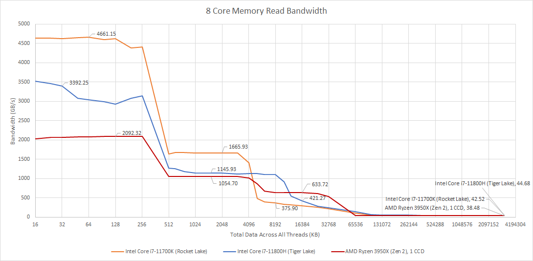
Rocket Lake and Tiger Lake make for an interesting comparison. Both benefit from AVX-512, but Tiger Lake ends up with lower bandwidth in L1 and L2 because of its lower clock speed. Two years after Sunny Cove’s “launch”, Intel’s 10nm process still had not matured enough to match its older 14nm process. The big 1280 KB, 20-way associative L2 would not help clocks either. In L3, Tiger Lake does regain some ground, and lands somewhere between Rocket Lake and Zen 2. So, Intel’s redesigned L3 ends up trading latency for increased capacity and bandwidth.
Sunny Cove versus Zen 2
Sunny Cove was supposed to be Zen 2’s contemporary. Chips using both architectures became available in 2019, so let’s go back up and have a high level look at how the architectures compare.
In almost all areas, Sunny Cove is much bigger while being just as “smart”. If AMD had to compete against this core in 2019, they would have had a much harder time.
Conclusion
Intel’s Sunny Cove architecture is a worthy follow on to Skylake. It brings a comprehensive pipeline upgrade that makes previous Intel architecture iterations look small. Intel claims that’s good for a 18% IPC increase, which is nothing to scoff at if their new process node allowed the new architecture to maintain Skylake’s clocks while keeping power consumption in check.
But that brings us to the elephant in the room. Intel’s 10 nm process failed the architecture, and did so in dramatic fashion. Sunny Cove’s 2019 launch was limited to quad core parts that only went up to 4.1 GHz. That’s fine for thin and light laptops, but meant Intel’s new architecture was missing in action everywhere else. Because of 10 nm process issues, there were no parts with higher core counts, higher clocks, or power targets beyond 28W.
To make things worse, AMD exists. Zen 2 launched in 2019 with a full lineup of desktop chips. With Sunny Cove unable to reach high clocks on 10 nm, Intel was left trying to contest the desktop market with yet another Skylake refresh – Comet Lake. Comet Lake pushed Skylake as far as it would go, boosting clocks to 5.3 GHz while bumping core count to 10. That left Intel clinging to a shrinking single-threaded performance lead, while 16 core Zen 2 parts on TSMC’s 7 nm process shredded Intel’s best desktop parts in multithreaded loads. And thanks to a process node advantage, Zen 2 could do so at much lower power.
In 2021, Intel finally brought Sunny Cove to the desktop. Apparently, 10 nm still couldn’t reach required clock speeds in 2021, so Sunny Cove was backported onto Intel’s more mature 14 nm process. This backported core was called Cypress Cove, and the desktop product was named Rocket Lake. Rocket Lake hit 5.3 GHz and finally gave a performance per core jump over Skylake.
But as we all know, Rocket Lake failed to lift off. Sunny Cove’s ambitious changes were made with 10 nm’s density and power improvements in mind. This is most apparent when core structures became more complex with no additional pipeline stages. For example, branch predictor pattern recognition and target tracking improved, but taken branch latency (in cycles) went down. The store forwarding mechanism no longer splits checks into two stages, but store forwarding latency stays at 5 cycles.

When Sunny Cove got ported back to 14nm, all the tuning done to give the core a good balance between performance, power, and area went straight out the window. Cypress Cove cores were large and drew tremendous amounts of power. That limited Rocket Lake to eight cores, giving AMD the multithreaded performance win by default. And because Rocket Lake launched so late, it went up against AMD’s Zen 3 architecture. Zen 3’s clock speed and performance per clock boost over Zen 2 left Rocket Lake with no market. Three years after Sunny Cove’s announcement at Intel’s 2018 architecture day, it was still getting the rug pulled from under it by 10 nm process shortcomings.
But in an alternate universe where Intel’s 10 nm process matured in time, AMD would have struggled to gain market share. Zen 2 is a solid core, but lacks Sunny Cove’s large structure sizes and AVX-512 support. It also can’t clock above 5 GHz, the way Golden Cove did on the mature 10nm process. A Sunny Cove launch across the entire product stack in 2019, with 5+ GHz clocks and eight to ten cores on desktop would have created a repeat of the Zen 1 versus Skylake scenario. Intel would hold a commanding advantage in thread-limited scenarios. AMD’s 16 core parts would still lead in well-multithreaded apps, but not by the same margin.
Sunny Cove was key to maintaining Intel’s high performance CPU superiority. Unfortunately for Intel, Sunny Cove never shook off the shackles of 10 nm failures. And fortunately for AMD, Sunny Cove wasn’t allowed to shine while Zen 2 made its presence felt.
If you like our articles and journalism and you want to support us in our endeavors then consider heading over to our Patreon or our PayPal if you want to toss a few bucks our way or if you would like to talk with the Chips and Cheese staff and the people behind the scenes then consider joining our Discord.
Credits
A lot of the comparisons here wouldn’t be possible without effort from people who contributed test results and the banner image is from the amazing Fritzchens Fritz.

Revisions
Tiger Lake has 1280 KB of L2. This was erroneously listed as 2 MB in a few places, and was fixed (6-7-2022)
Added used memory specifications for the contributed data and refomated the test results chart (6-7-2022)