
Intel’s Ambitious Meteor Lake iGPU

Intel and AMD both tried to ship iGPUs fast enough to compete with low end discrete cards over the past 10 years with mixed results. Recently though, powerful iGPUs have been thrown back into the spotlight. Handhelds like Valve’s Steam Deck and ASUS’s ROG Ally demonstrated that consumers are willing to accept compromises to play games on the go. AMD has dominated that market so far. Valve’s Steam Deck uses AMD’s Van Gogh APU, and the ROG Ally uses the newer Phoenix APU. Unlike Van Gogh, Phoenix is a general purpose mobile chip with both a powerful CPU and GPU. Phoenix doesn’t stop at targeting the handheld segment, and threatens Intel’s laptop market share too.

In response, Meteor Lake brings a powerful iGPU to the party. It has the equivalent of 128 EUs and clocks up to 2.25 GHz, making it modestly wider and much faster than Raptor Lake’s 96 EU, 1.5 GHz iGPU. Raptor Lake’s Xe-LP graphics architecture gets replaced by Xe-LPG, a close relative of the Xe-HPG architecture used in Intel’s A770 discrete GPU. At the system level, Meteor Lake moves to a GPU integration scheme that better suits a chiplet configuration where the iGPU gets significant transistor and area budget.
I’ll be testing Meteor Lake’s iGPU with the Core Ultra 7 155H, as implemented in the ASUS Zenbook 14. I purchased the device myself in late February.
System Level
Intel iGPUs were traditionally attached to the rest of the system via a stop on the CPU’s ring bus interconnect. GPU memory requests would go through the ring bus and L3 cache, just like CPU memory requests. When this scheme first debuted in Sandy Bridge, the iGPU didn’t have enough transistor budget for a big cache of its own. CPU performance was a priority at that time and needed a big L3 cache anyway, so leveraging the CPU’s L3 made a lot of sense. But doing so created a pile of problems.

GPU memory accesses would take the ring bus and L3 out of a low power state. Cache design became a compromise because low latency is more critical for CPUs than GPUs. A dedicated GPU cache could save power by having higher latency, but Intel couldn’t hurt latency on a cache primarily meant to serve the CPU. Intel mitigated some of these issues by decoupling the ring bus clock from the CPU core clock in Haswell, but the shared last level cache would always see compromises because CPUs and GPUs have different needs.

Meanwhile, Intel’s client chips have been getting more accelerators. The company put GNA (a small AI inference accelerator) and an image processing unit into the system agent, but that scheme always seemed like more of a hack than an elegant solution. Meteor Lake therefore adds a new “Scalable Fabric” that can host a variety of accelerators and give them full access to memory bandwidth.

Intel also switched to a chiplet design in order to use different process nodes depending on each accelerator’s needs. Meteor Lake’s iGPU tile for example uses TSMC’s 5nm node. But switching to a chiplet design means iGPU-private cache misses have to cross die boundaries. Cross-die transfers cost more energy and latency than talking within a monolithic die. Accessing the CPU’s L3 from the iGPU would require crossing two die boundaries.
Therefore, Intel abandoned the shared L3. The iGPU moves off the CPU’s ring bus and onto this Scalable Fabric. To accompany this change, the GPU uses the iCXL protocol to talk to the rest of the system instead of IDI. I wrote another article on Meteor Lake a couple years ago that covers the switch from IDI to iCXL in more detail. Here, I’ll focus on Meteor Lake’s iGPU architecture.
GPU Organization
Xe Cores are basic building blocks for Meteor Lake’s iGPU, and trace their ancestry to Subslices in prior Intel iGPUs. The Core Ultra 7 155H’s iGPU has eight Xe Cores split across two Render Slices. Like AMD’s similar “Shader Array” subdivision, a Render Slice includes fixed function graphics hardware like rasterizers and ROPs.

Multiple Slices or Shader Arrays let designers scale geometry and pixel throughput to keep those figures in balance with higher compute throughput. Xe’s Render Slices don’t include an extra cache level like AMD’s Shader Array, but the two GPUs otherwise have a surprisingly similar two-slice arrangement.

From another angle, Meteor Lake’s iGPU is like 1/4 of Intel’s A770.
Compute Architecture
Intel’s Xe-LPG architecture packs 128 FP32 lanes into each Xe Core, with a setup similar to the Xe-HPG architecture used in Intel’s Arc A770. The Xe Core is subdivided into 16 “Vector Engines” (XVEs), giving it more partitions than AMD’s RDNA 3 Workgroup Processor (WGP) or Nvidia’s Ada Streaming Multiprocessor (SM).

Xe-LPG’s XVEs use a combination of long vectors and thread level parallelism to hide memory latency. A XVE can have up to eight threads in flight. Unlike AMD and Nvidia architectures, Intel statically allocates register file capacity for in-flight threads. Every thread gets 128 registers, regardless of whether it needs them all. Occupancy (live threads) can’t be limited by register file capacity. In contrast, AMD and Nvidia allocate register file capacity based on how many registers each thread uses. Occupancy on AMD’s RDNA 3 architecture can decrease from its maximum of 16 threads per SIMD depending on per-thread register usage.
Like other Intel graphics architectures, Xe-LPG’s vector width ranges from 1-wide to 32-wide and is specified per-instruction. For comparison, AMD’s RDNA architecture can use 32 or 64 wide vectors, but vector width is fixed for an entire GPU program (kernel). In both cases, large vectors let one instruction apply across many data elements, reducing fetch, decode, and instruction control costs.

But vectors aren’t free. If some lanes within a vector take different branch directions, GPUs execute both sides of the branch and disable execution unit lanes to ensure correct results, reducing compute throughput. Such divergence penalties typically disappear once all threads within a vector go in the same direction.

Xe-LPG however can suffer divergence penalties with SIMD16 instructions even when contiguous, aligned blocks of 16 lanes take the same branch direction. That’s because “pairs of vector engines run in lockstep” to reduce thread control costs. Intel wasn’t specific about this, but I believe paired XVEs must execute the same instruction, so branch divergence across a XVE pair has to be handled by disabling lanes. Even if one of the XVEs has all of its lanes disabled for the instruction being issued, it can’t independently fetch another instruction to feed its execution units.
Execution Units
A XVE’s math execution units are split across two ports. Port 0 handles the most common FP32 and FP16 operations. Port 1 serves to offload integer and special function operations, keeping Port 0 free for floating point math. Rare operations like FP64 math are also offloaded to Port 1. Separate Send and Branch ports handle memory accesses and control flow.
Unlike Xe-LP, which splits FP32 units across Port 0 and Port 1, Xe-LPG’s execution port layout lets it reach full FP32 full throughput without dual issue. It’s basically the same idea as Xe-HPG, just without the matrix multiplication units that would have been present on Port 2.

Xe-LPG likely uses the same multi-issue scheme as GCN and older Intel iGPU architectures. Thread control logic can select up to four instructions per cycle from four different threads in order to fill the available execution ports. That preserves in-order scalar execution within each thread. Unlike RDNA 3’s dual issue scheme, Intel relies on high occupancy and thread level parallelism to keep both math ports fed. Comparing the Core Ultra 7 155H’s iGPU with the one in AMD’s Phoenix is hard because results can vary heavily depending on compiler code generation.

AMD’s Phoenix can easily pull ahead when it can leverage RDNA 3’s dual issue capabilities. Intel’s GPU architecture enjoys strong integer multiplication performance, and can gain an edge when RDNA 3 runs in wave32 mode but can’t dual issue. The two GPUs are generally evenly matched, with discrepancies explained by compiler/driver weirdness.

half8 (FP16) types.For example, Intel’s low FP16 FP throughput is because the compiler cannot generate FP16 fused multiply add instructions. I tried using OpenCL’s mad() function, which lets the driver prefer speed over accuracy, but got the same results. Both AMD and Intel’s compilers made a mess out of char16 (INT8) adds. AMD emitted INT16 adds and used bitwise operations to generate 8-bit results. Intel mixed in a pile of register-to-register MOVs between INT8 adds.
Compilers are great and necessary, and I can hate them at the same time.
Cache and Memory Access
Any GPU needs a competent cache hierarchy to keep its execution units fed. Consumer iGPUs face an even greater challenge because they share a narrow memory bus with the CPU. LPDDR5 provides more bandwidth than DDR3 or DDR4, but the Core Ultra 7 155H still doesn’t enjoy the bandwidth to compute ratios that low end discrete GPUs do.

Xe-LPG’s data cache hierarchy starts within each Xe Core, and strongly resembles Xe-HPG. A 192 KB block of storage can be split for use as local memory (SLM, or Shared Local Memory in Intel terms) or L1 cache. Texture fetches use a separate sampler cache. Among current generation GPUs, Intel and Qualcomm still use dedicated, read-only texture caches. AMD and Nvidia use a unified cache to serve both data and texture accesses.
Local Memory
GPUs cores feature fast, software managed local memory. Programs have to explicitly move data into local memory. But once they do so, they enjoy guaranteed low latency and high bandwidth access to that data. On the hardware side, local memory is directly addressed and only shared by a specific group of threads (a workgroup). That removes the need for virtual to physical address translation or mechanisms to ensure coherency across multiple GPU cores. As mentioned before, Xe-LPG’s local memory and L1 cache use the same backing storage.

Xe-LPG’s local memory latency is par with older, lower clocked Nvidia GPUs like the GTX 980 Ti. It’s decent performance, but recent AMD and Nvidia GPUs do better. We can also measure latency by using local memory to exchange data between threads.

Intel doesn’t do so well when handling atomic operations, though 40.6 ns isn’t bad in an absolute sense. Again, AMD and Nvidia offer better performance.
AMD’s Phoenix and Meteor Lake offer surprisingly similar bandwidth to local memory. Both architectures appear to have a 128 bytes per cycle of local memory bandwidth per building block (Xe Core or WGP). AMD’s higher clock speed is balanced out by Intel having eight Xe Cores to Phoenix’s six WGPs, and possibly by bank conflicts on AMD’s side. I don’t have a Phoenix device, so I relied on others to test and couldn’t check device clocks or whether AMD’s driver chose WGP mode (128 KB of local storage shared by both CUs) or CU mode (each half of the 128 KB serves a CU).

Integrated graphics have come a long way, and it’s impressive to see standard iGPUs on AMD and Intel’s mobile chips surpass that of Nvidia’s GTX 1050 3 GB. Still, these iGPUs are far away from offering a premium gaming experience and cannot compete with larger discrete cards.
Cache Hierarchy
Local memory is difficult to use, so a lot of GPU programs don’t bother with it. Caches are more useful because they don’t require software to explicitly move data around. Xe-LPG gets a cache hierarchy designed to feed a powerful iGPU while avoiding DRAM limitations
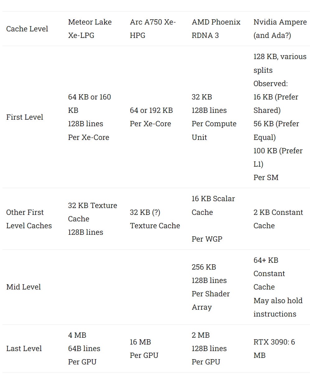
Data accesses first hit a 192 KB block of storage, though not all of it can be used as L1. Even without local memory allocated, I was only able to access up to 160 KB with low latency, leaving 32 KB unaccounted for.

I couldn’t use the last 32 KB as local memory either. Allocating any local memory drops L1 capacity to 64 KB. I then tested local memory capacity across the GPU by checking how much I could allocate across a lot of workgroups before some could no longer execute in parallel.

768 KB would be 96 KB per Xe Core, so the last 32 KB is still missing. Perhaps Intel reserves it for fixed function hardware. Intel’s Xe-HPG architecture from the A750 can use all 192 KB as L1 cache.

Xe-LPG has a separate texture cache. Accesses with OpenCL’s image1d_buffer_t type show a latency bump after 32 KB on both A750 and Meteor Lake’s iGPU, though Intel’s documentation suggests Xe-HPG has 64 KB texture caches. Both the L1 data and texture caches use 128B cachelines. Texture cache accesses have slightly higher latency.

Meteor Lake’s iGPU has similar L1 latency to Intel’s A750. I suspect Xe-LPG and Xe-HPG have a lot in common. Xe-LPG has similar L1 latency to AMD’s RDNA 3 while offering several times as much L1 caching capacity. RDNA 3’s mid-level 256 KB cache can compensate for low L0 capacity, but does take a bit longer to get to than L0 or Intel’s L1. Nvidia’s Ada architecture has just above 14 ns of L1 latency, so Intel trades latency for higher caching capacity when compared to Nvidia.

After L1, Meteor Lake has a 4 MB L2 cache shared across the GPU. It’s smaller but lower latency than the A750’s 16 MB cache. Compared to AMD, it offers similar latency but twice as much cache capacity. 4 MB is a lot of last level cache for an iGPU. For comparison, Nvidia’s RTX 3070 has the same L2 capacity.
Bandwidth
Meteor Lake’s iGPU has a lot of bandwidth, but RDNA 3 is a bit ahead. AMD’s 256 KB L1 cache does an impressive job because it’s a shared cache, but offers similar bandwidth to Meteor Lake’s eight Xe-Core private L1 caches. Assuming no change from RDNA 1, the mid-level L1 cache can deliver 4×128 bytes per cycle if there are no bank conflicts.

AMD’s Phoenix has a slight L2 bandwidth advantage too, but again Intel compensates by having a larger L2. Meteor Lake and Phoenix have similar DRAM bandwidth, though Meteor Lake is slightly ahead thanks to faster memory.
Global Memory Atomics
Programs sometimes have to synchronize threads across the GPU using atomic operations on global memory locations. That’s usually slower than doing so through local memory, but global memory is a lot more flexible because it’s shared across the entire GPU.

Meteor Lake’s iGPU again turns in a decent performance. Using OpenCL’s atomic_cmpxchg function to move data between threads shows similar latency to pointer chasing in the L2, so atomics are probably handled there. I never got the test run on AMD’s Phoenix, so I’m using the RX 6900 XT for reference. AMD’s large RDNA 2 GPU performs very well in this test.
CPU to GPU Copy Bandwidth
Compared to their discrete counterparts, iGPUs are often hamstrung by a small memory bus and low area and power budget. All of that has to be shared with the CPU as well. But iGPUs aren’t limited by PCIe bandwidth, meaning they can transfer data very quickly between CPU and GPU memory spaces. Meteor Lake’s iGPU easily beats a PCIe 3.0 x16 connection. But earlier Intel iGPUs are still faster at small copy sizes because they can keep data transfers within the CPU’s L3 cache.

Both Meteor Lake and Phoenix see lower bandwidth at smaller copy sizes. GPUs typically handle such data transfers by handing them off to DMA engines. These DMA engines can tolerate memory latency very well, but can take a while to set up and get the transfer started. Synchronization is also needed after a copy because DMA engines operate independently of the CPU’s cores or the CPU’s shader array. I suspect a good chunk of total copy time is taken up by start/stop latency at small test sizes.

At larger copy sizes, where start/stop latency takes up less time compared to actually doing the transfer, Meteor Lake pulls ahead thanks to higher bandwidth LPDDR5 memory.
Final Words
Meteor Lake abandons the familiar Sandy Bridge client design that characterized Intel’s consumer CPU offerings for more than a decade. In its place, we get a flexible chiplet strategy that lets Intel pile on accelerators in response to market demands. Meteor Lake’s Arc iGPU is one of those accelerators, and is arguably the most important one. Consumers in 2024 expect passable gaming performance from ultraportable devices. GPUs can also accelerate a variety of non-graphics workloads, including machine learning.
Therefore, Meteor Lake gets a formidable iGPU. Besides going wider and faster, Meteor Lake’s iGPU architecture shares a lot in common with Arc A770’s. Intel is signaling that they’re serious about competing in the iGPU space.

AMD is Intel’s most obvious competitor, since Nvidia doesn’t compete in the PC gaming iGPU space. Coincidentally, Intel’s iGPU strategy has shifted to resemble AMD’s. AMD’s Phoenix uses RDNA 3, a desktop first GPU architecture. Phoenix also positions the GPU as one of many accelerators attached to a flexible fabric. Like Intel’s Scalable Fabric, AMD’s Infinity Fabric provides enough bandwidth to handle DRAM traffic, but doesn’t have low enough latency to deal with CPU to cache traffic. Neither Meteor Lake nor Phoenix attempt to share the CPU’s L3 cache with the iGPU.
The Radeon 780M in AMD’s Phoenix provides slightly more compute throughput and cache bandwidth than Meteor Lake’s Arc iGPU, though the difference isn’t huge. Meanwhile, Meteor Lake benefits from higher cache capacity. I don’t have a Phoenix device and won’t be making direct performance comparisons. Regardless of how the two iGPUs compare, Intel is serious about delivering competitive iGPUs. 4.5 TFLOPS in a thin and light design is nothing to sneeze at. And at first glance, Intel has done a good job of supporting that compute throughput.
Overall, Meteor Lake’s iGPU is a competent offering that should keeps Intel in the iGPU game. Even if it can’t beat AMD’s Phoenix, it should serve as a solid springboard for Intel’s future iGPU efforts.
If you like our articles and journalism, and you want to support us in our endeavors, then consider heading over to our Patreon or our PayPal if you want to toss a few bucks our way. If you would like to talk with the Chips and Cheese staff and the people behind the scenes, then consider joining our Discord.