
Examining AMD’s RDNA 4 Changes in LLVM

As 2024 continues on, because time never stops, AMD has been working on their upcoming RDNA 4 architecture. Part of this involves supporting open source projects like LLVM. If done right, merging these changes early will ensure RDNA 4 will be well supported on launch. Because components like LLVM are open source, we can see these changes and get a preview of what AMD is changing over RDNA 3.
LLVM is particularly interesting because it’s a compiler project, and is used to compile source code into machine code for various architectures. The compiler has to be told how the ISA works in order to generate working code, so AMD has to add RDNA 4’s ISA changes in LLVM.
Terminology
AMD refers to their GPUs in several different ways. RDNA 3 and 4 refer to the architecture, but individual implementations of the architecture get a “gfx{number}” moniker. For example, the RX 7900 XTX target in LLVM is gfx1100, and the RX 6900 XT is gfx1030. For that reason, RDNA 3 and RDNA 2 are referred to as GFX11 and GFX10 respectively. In LLVM, RDNA 4 is referred to as GFX12.
LLVM code so far references gfx1200 and gfx1201 implementations of RDNA 4. These likely correspond to two different dies. AMD has a habit of giving different GPU architecture implementations distinct compiler targets. For example, the RX 6900 XT gets targeted with gfx1030 while the RDNA 2 integrated iGPU in Zen 4 desktop CPUs is gfx1036.
More Explicit Barriers
AMD GPUs resolve memory dependencies with explicit waits. For example, s_waitcnt vmcnt(0) would wait for all vector memory loads to finish, ensuring their results are available for subsequent instructions. Up to RDNA 3, AMD has several special registers that track the number of outstanding accesses in a specific category.

RDNA 4 takes the categories above and breaks them down into more specific ones. With this move, AMD makes a dramatic change in their memory dependency handling scheme that had been in place since the original GCN architecture.
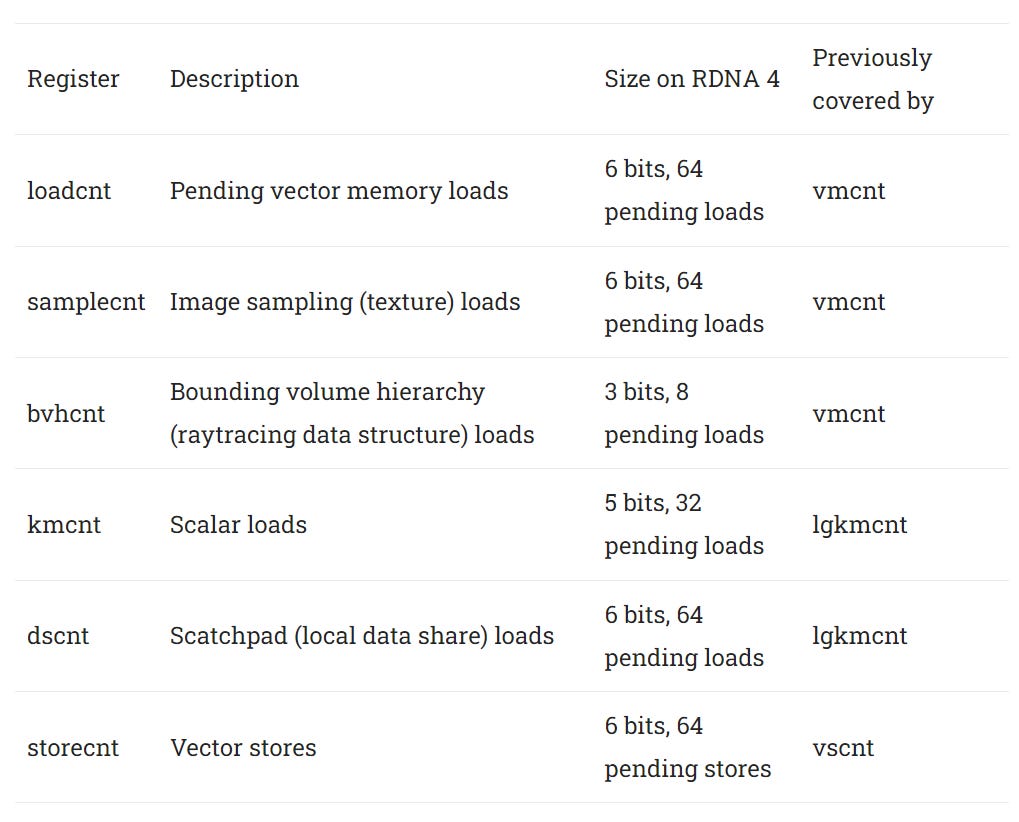
Shader programs on RDNA 4 will be able to wait on memory accesses with better granularity. I feel like this change was done to make the ISA cleaner rather than significantly improve performance. GPUs use in-order execution and have high cache (and memory) latencies compared to CPUs, so individual threads will stall quite often due to memory latency. Perhaps this change in RDNA 4 will let threads extract a bit more instruction level parallelism by waiting on a false dependency less often.
Nvidia GPUs since Maxwell use a different scheme where six barriers can be flexibly assigned to wait on any access. It’s even more flexible than RDNA 4’s scheme because multiple barriers can be assigned to different accesses of the same category. However, the limited number of barriers (6) could be a limitation for Nvidia.
More Flexible Coherency Handling
Like CPUs, GPUs have to solve the problem where different cores have private caches but may need to make writes visible to each other. Up to RDNA 3, memory access instructions had a GLC bit that could be set to make them globally coherent. If the GLC bit is set for a load, it will intentionally miss in RDNA’s L0 and L1 caches, and go straight to L2. That’s because each L0 or L1 cache instance only services a Compute Unit or Shader Engine, respectively. By reading from L2, the instruction can be sure that it sees a write done by a thread running in another Shader Engine.

Similarly, the SLC (System Level Coherent) and DLC (Device Level Coherent) bits control L2 and Infinity Cache behavior respectively. Besides skipping cache levels, the GLC/SLC/DLC bits also provide non-temporal hints to RDNA’s caches. Non-temporal means the program is unlikely to reuse the data, so hardware should prefer to not keep it in cache. Such hints don’t necessarily evict the accessed data from cache. For example, RDNA’s L2 cache handles hits from streaming (non-temporal) accesses by leaving the line in cache, but not updating its LRU bits. Thus the line is more likely to be evicted in the future to make room for new data, but isn’t kicked out immediately.
RDNA 4 rearranges the cache policy bits to control the Shader Engine’s L1 cache separately. Non-temporal hints are separated out as well. Instead of using three bits (GLC/SLC/DLC), RDNA 4 controls cache behavior with four bits. Three provide temporal hints, and two specify the scope

RDNA 4 could use its finer grained cache control to pass data between threads or kernel invocations through the L1 rather than doing so at L2. The Shader Engine’s L1 is much faster than the GPU-wide L2 on all RDNA generations, so taking advantage of that L1 cache whenever possible is a worthy goal. If setting the scope to SE lets RDNA 4 avoid L1 invalidations, AMD could gain some performance from higher L1 hitrates. But it could be hard to pull off as well, because any dependent thread will have to be launched on the same SE.
Temporal hints are given on RDNA 4 using three separate bits, rather than being implied via the SLC/DLC/GLC bits as before.
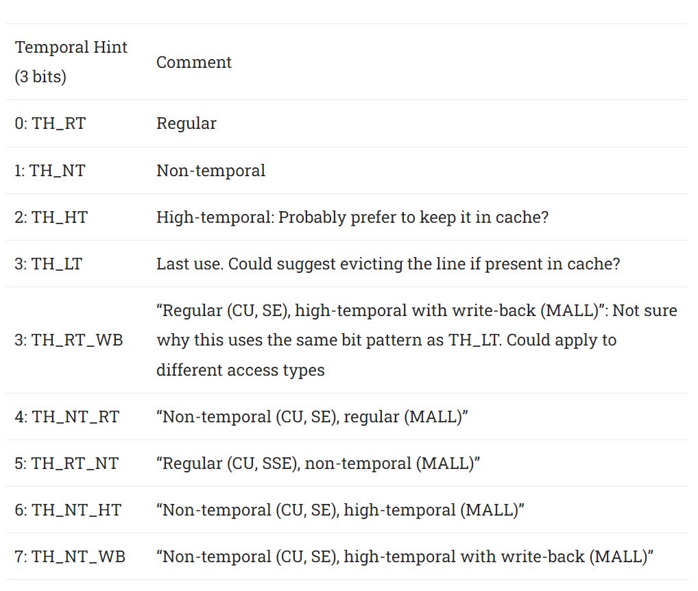
RDNA 4 introduces high-temporal options too. High temporal likely signifies code expects to reuse the accessed data soon, so the cache should prefer to keep it stored. Just as with non-temporal hints, the hardware doesn’t have to act in a well defined way when it sees a high-temporal hint. For example, it could artificially keep the high-temporal line in the LRU position for a number of accesses regardless of whether it’s hit. Or, it could do nothing at all.
Better Tensors
AI hype is real these days. Machine learning involves a lot of matrix multiplies, and people have found that inference can be done with lower precision data types while maintaining acceptable accuracy. GPUs have jumped on the hype train with specialized matrix multiplication instructions. RDNA 3’s WMMA (Wave Matrix Multiply Accumulate) use a matrix stored in registers across a wave, much like Nvidia’s equivalent instructions.

RDNA 4 carries these instructions forward with improvements to efficiency, and adds instructions to support 8-bit floating point formats. AMD has also added an instruction where B is a 16×32 matrix with INT4 elements instead of 16×16 as in other instructions.

Machine learning has been trending towards lower precision data types to make more efficient use of memory capacity and bandwidth. RDNA 4’s support for FP8 and BF8 shows AMD doesn’t want to be left out as new data formats are introduced.
Sparsity
Moving to lower precision data formats is one way to scale matrix multiplication performance beyond what process node and memory bandwidth improvements alone would allow. Specialized handling for sparse matrices is another way to dramatically improve performance. Matrices with a lot of zero elements are known as sparse matrices. Multiplying sparse matrices can involve a lot less math because any multiplication involving zero can be skipped. Storage and bandwidth consumption can be reduced too because the matrix can be stored in a compressed format.
RDNA 4 introduces new SWMMAC (Sparse Wave Matrix Multiply Accumulate) instructions to take advantage of sparsity. SWMMAC similarly does a C += A * B operation, but A is a sparse matrix stored in half of B’s size. A sparsity index is passed as a fourth parameter to help interpret A as a full size matrix. My interpretation of this is that the dimensions in the instruction mnemonic refer to stored matrix sizes. Thus a 16x16x32 SWMMAC instruction actually multiplies a 32×16 sparse matrix with a 16×32 dense one, producing a 32×32 result.

If I guessed right, SWMMAC instructions would be the same as their WMMA siblings, but produce a result matrix twice as long in each dimension.
Of course there’s no way to infer performance changes from looking at LLVM code, but I wonder if AMD will invest in higher per-SIMD matrix multiplication performance in RDNA 4. RDNA 3’s WMMA instructions provide the same theoretical throughput as using dot product instructions.
[WMMA] instructions work over multiple cycles to compute the result matrix and internally use the DOT instructions
“RDNA 3” Instruction Set Architecture Reference Guide
Since SWMMAC takes a sparse matrix where only half the elements are stored, perhaps RDNA 4 can get a 2x performance increase from sparsity.
Software Prefetch
GPU programs typically enjoy high instruction cache hitrate because they tend to have a smaller code footprint than CPU programs. However, GPU programs suffer more from instruction cache warmup time because they tend to execute for very short durations. RDNA 3 mitigates this by optionally prefetching up to 64x 128-byte cachelines starting from a kernel’s entry point. RDNA 4 increases the possible initial prefetch distance to 256 x 128 bytes. Thus code size covered by the initial prefetch goes from 8 KB to 32 KB.
Once a kernel starts, the Compute Unit or Workgroup Processor frontend continues to prefetch ahead in the instruction stream. Prefetch distance is controlled by an instruction in the shader program. Up to RDNA 3, AMD GPUs could be told to prefetch up to three 64B cachelines ahead of the currently executing instruction.

s_set_inst_prefetch_distance instruction telling hardware to prefetch 3 cachelines ahead of the program counterAs far as I know, prefetching only applies to the instruction side. There’s no data-side prefetcher, so RDNA 3 SIMDs rely purely on thread and instruction level parallelism to hide memory latency.
RDNA 4 adds new instructions that let software more flexibly direct prefetches, rather than just going in a straight line. For example, s_prefetch_inst could point instruction prefetch to the target of a probably taken branch. If my interpretation is correct, RDNA 4 could be better at handling large shader programs, with instruction prefetch used to reduce the impact of instruction cache misses.

On the data side, RDNA 4 appears to introduce software prefetch instructions as well. GPUs typically don’t do any prefetching, and use a combination of wide accesses and thread level parallelism to achieve high bandwidth. In contrast, CPUs often run programs with little explicit parallelism and can benefit greatly if prefetch reduces program-visible memory latency.
But maximizing performance isn’t a black and white thing, and GPU code can be latency limited even with a lot of threads in flight. In those cases, prefetch could be a promising strategy as long as there’s bandwidth to spare. One hypothetical example might be prefetching all the children of nodes several levels ahead in a raytracing kernel.
Sub 32-bit Scalar Loads
Graphics workloads typically use 32-bit data types, but compute workloads use all sorts of data widths. AMD’s GPUs had flexible load widths on the vector side for a while, but the scalar path was restricted to 32-bit or larger loads. RDNA 4 changes this by adding 8-bit and 16-bit scalar load instructions.

This change is mostly about making the ISA nicer for compute programs that use 8 or 16-bit data types. On prior AMD GPU generations, you can achieve similar results by loading a 32-bit value and masking off the high bits.
Final Words
GPU instruction sets are more fluid than CPU ones because developers don’t ship GPU binaries. Rather, GPU drivers compile source (or intermediate) code into GPU binaries on the user’s machine. Thus GPU makers can change the GPU ISA between generations without breaking compatibility, so long as they update their drivers to handle the new ISA.
Thus a GPU’s ISA is often more closely tied to hardware than a CPU’s ISA. Looking at GPU ISA changes shows how far GPUs have come from the days when they were pure graphics processors. Over the past couple decades, GPUs got flexible branching, support for standard IEEE floating point formats, scalar datapaths, and specialized matrix multiplication instructions.
RDNA 4 continues AMD’s GPU ISA evolution. Software prefetch and more flexible scalar loads continue a trend of GPUs becoming more CPU-like as they take on more compute applications. AI gets a nod as well with FP8 and sparsity support. Better cache controls are great to see as well, and more closely match the ISA to RDNA’s more complex cache hierarchy.
Finally, remember nothing is final until a RDNA 4 product is released. All the information here is preliminary. Reading code in an unfamiliar project can be hard too, so there’s a chance I made a mistake somewhere. I highly encourage you to go through the LLVM source code yourself. To make that easier, I’ve sprinkled links to the appropriate files on Github throughout the article. Have fun!
If you like our articles and journalism, and you want to support us in our endeavors, then consider heading over to our Patreon or our PayPal if you want to toss a few bucks our way. If you would like to talk with the Chips and Cheese staff and the people behind the scenes, then consider joining our Discord.