
Maxwell: Nvidia’s Silver 28nm Hammer

Nvidia’s Kepler architecture gave the company a strong start in the 28nm era. Consumer Kepler parts provided highly competitive gaming performance and power efficiency. In the compute market, Kepler had no serious competition thanks to the strong CUDA software ecosystem. Any successor to Kepler had some big shoes to fill.

That’s where Maxwell comes in. Even though Kepler had performed well, it had room for improvement. Mediocre compute throughput and memory bandwidth placed Kepler at a disadvantage at higher resolutions. Kepler’s area efficiency wasn’t great either. Maxwell looks to correct those shortcomings.
Overview
Maxwell’s basic building block is the Streaming Multiprocessor (SM). Compared to Kepler, Maxwell cuts down a SM’s capabilities in exchange for getting more of them onto a die. GM204, a midrange Maxwell part, uses 16 SMs to provide 2048 total FP32 lanes. For comparison, Kepler’s GK104 die occupied the same market segment. GK104 uses 8 SMs to provide 1536 FP32 lanes. Both GM204 and GK104 have four rasterizer partitions or GPCs (Graphics Processing Clusters), so GM204 has more SMs per rasterizer.

At the high end, GM200 has 24 SMs for 3072 lanes. High end Kepler parts used GK110 or GK210 chips, which had 15 SMs for 2880 FP32 lanes. Maxwell therefore gets a slight increase in theoretical compute throughput, but that’s not where Nvidia’s focus is. Rather, the company is spreading that compute power across more SMs, letting the GPU as a whole keep more work in flight and better keep the execution units fed.
Maxwell’s SM: Trimming the Fat
Like Kepler, Maxwell’s SM consists of four SM sub partitions (SMSPs), each with a 16 entry scheduler and a 64 KB register file. But Nvidia cut down on rarely utilized execution resources to reduce SM area and power.

First, Nvidia’s engineers dropped provision for high FP64 throughput. Kepler could be configured with FP64 rates as high as 1:3 of FP32 rate, like in GK210. Nvidia likely accomplished this by laying out a Kepler SM so that each SMSP could be extended with extra execution units. GK210 and GK110 Kepler dies took advantage of this and could turn in a formidable performance for FP64 code. Maxwell drops this ability, clustering the four SMSPs around the center part of the SM with control logic and Shared Memory. The revised layout reduces average distance between execution units and caches, but makes it hard to pack in extra FP64 units without redoing the layout. All Maxwell SKUs have a 1:32 FP64 rate including datacenter SKUs like the Tesla M60.
Next, Nvidia went after Kepler’s shared FP32 units. Besides having a 32-wide private FP32 execution unit, Kepler’s SMSPs could call on an additional 32-wide FP32 unit shared by another SMSP. But those shared FP32 units required dual issue to utilize. That in turn required Nvidia’s compiler to discover instruction level parallelism (ILP) and explicitly mark instructions for dual issue. Then, Kepler would have to feed both instructions with a register file only capable of handling four reads per cycle. Reaching peak FP32 rate would require fused multiply-add (FMA) instructions, which require 3 inputs.

Thus Kepler would have to rely heavily on the operand collector to find register reuse or forwarding opportunities to get around register file bandwidth limits. That task would get harder in the face of register bank conflicts.
The Kepler approach of having a non-power of two number of CUDA cores, with some that are shared, has been eliminated.
Whitepaper, Nvidia GeForce GTX 750 Ti
Finally, GPUs often don’t make full use of their execution units. GPUs have high memory access and execution latency. They can hide that to some extent with thread level parallelism, but even that may not be enough. If your execution units spend a lot of time idle anyway, there’s little point in having more of them.

With the shared FP32 units dropped, a Maxwell SM can achieve maximum throughput without dual issue. Maxwell can still dual issue, but dual issue now focuses on reducing dispatch bandwidth consumed by supporting operations. Memory accesses, special functions, conversions, and branches can be issued alongside a vector FP32 or INT32 instruction.

From profiling games with Pascal, which has a similar dual issue mechanism, about 5-15% of instructions are typically dual issued. Thus dual issue mainly serves to provide a minor increase in per-SM performance in compute bound sequences. As with Kepler, the compiler is responsible for marking dual issue pairs.
Static Scheduling Improved
Maxwell uses a static scheduling scheme much like Kepler’s, with compiler-generated control codes specifying stall cycles to resolve dependencies from fixed latency instructions and explicitly marking dual issue opportunities. But Maxwell extends Kepler’s control codes to cover register file caching and more flexible barriers. Per-instruction control information increases from 8 to 21 bits. In the instruction stream, Maxwell now has one 64-bit control word for every three instructions, compared to one every 7 instructions for Kepler.

Maxwell and Kepler both specify stall cycles with 4 bits to handle fixed execution latencies, but Maxwell uses additional bits to more flexibly handle variable latency instructions. Sources conflict on whether Kepler control codes include memory barriers, with Zhang et al. saying the high bits of an instruction’s control byte specify shared memory (software managed scratchpad), global memory, or texture memory dependency barriers3. Hayes et al. says Kepler control codes only include stall cycles and dual issue info4. I suspect Hayes is correct because I see texture dependency barriers in Kepler code, while those are gone in Maxwell. In any case, Kepler didn’t have fine grained barriers.

TEXDEPBAR). Maxwell assembly doesn’t have these explicit barriersMaxwell adds that capability by letting instructions associate a barrier with their result. Dependent instructions can then wait on barriers corresponding to the data they need, rather than waiting for memory accesses of a specific category to complete. This fine grained barrier capability likely uses a 6 entry per-thread scoreboard on Maxwell. It’s more complex than simply waiting for a memory access queue to drain but should be nowhere near as complex as Fermi’s register scoreboard.
Another four control code bits handle register caching. GPUs need massive register bandwidth, but register files need high capacity to keep a lot of work in flight, and low power at the same time. Most GPUs use banked register files to allow multiple accesses per cycle because multi-porting or duplication are expensive. Maxwell’s register file has four single-ported banks. That lets it handle four reads per cycle, but only if they go to different banks.

Kepler and prior Nvidia GPUs use an operand collector to schedule register reads around bank conflicts. Maxwell goes further with a compiler-managed register reuse cache. This cache has two entries for four operand positions, for eight total entries or 256 32-bit values. Four bits in the control code act as a bitmask. If a bit is set, the corresponding operand is saved into the cache. If a subsequent instruction can read from the register cache, it can avoid bank conflicts.

While this mechanism could let the compiler achieve more effective operand reuse, it has limitations. The register cache isn’t replicated per-thread and is invalidated when the scheduler partition switches between threads2. With just two entries per operand position, it’s also small. And caching values based on operand position means that some entries in the register cache won’t be used for instructions with fewer than four inputs.
Compute Throughput
Maxwell SMs may have fewer FP32 units, but Maxwell GPUs compensate by having more SMs running at higher clocks. The result is plenty of compute throughput. The Hawaii chip in AMD’s R9 390 is competitive against the largest Kepler die, the GK110. GM200, GK110’s successor, sails far ahead of Hawaii despite using the same 28 nm process.

Nvidia didn’t cut special function units, so Maxwell has a huge lead over Kepler for operations like reciprocals and inverse square roots. On AMD’s side, Hawaii still turns in a strong performance for integer throughput. FP64 is another notable strength. Even though Hawaii’s FP64 capabilities get cut back compared to Tahiti, Maxwell’s FP64 units got cut even more. So, Hawaii also pulls ahead with double precision operations. Unfortunately for AMD, neither of those categories are important for gaming workloads.
SM Memory Subsystem
A GPU needs a lot of bandwidth to feed wide vector units, so a SM has a beefy memory subsystem to do just that. The memory subsystem in Maxwell SMs is derived from Kepler’s, but Nvidia has rebalanced the SM’s caches and Shared Memory.

Shared Memory (OpenCL Local Memory)
GPU cores feature a small software managed scratchpad that offers consistently high bandwidth and low latency access, but is only visible within a group of threads. Nvidia refers to this as Shared Memory, which is a misnomer because only threads in the same workgroup (co-located in the same SM) can share data through Shared Memory. AMD has a slightly better name, calling their equivalent structure the Local Data Share, or LDS. OpenCL refers to this as Local Memory.
Maxwell adds integer atomic ALUs to the Shared Memory unit, dramatically improving performance when different threads have to ensure ordering or exchange data.
Maxwell improves upon this by implementing native shared memory atomic operations
On Kepler, software had to use a complex load with lock + store with unlock sequence. It’s a bit like how older Arm CPUs had to use load-acquire and store-release, resulting in higher “core-to-core” latencies until an atomic compare-and-swap instruction was added.

Atomics on Shared Memory suffered horrible latency on Kepler. Incredibly, they had even higher latency than global memory atomics, which were accelerated by atomic units in Kepler’s L2 cache. Maxwell fixes that by introducing a Shared Memory atomic compare and swap instruction.

AMD had hardware support for local memory atomics as far back as Terascale 2, and never did badly in this GPU thread-to-thread latency test. But Maxwell is a huge step forward and puts Nvidia ahead of AMD.
Local memory latency improves too thanks to Maxwell’s higher clocks. Kepler and Maxwell both have a latency of 34 cycles in this pointer chasing test, but the EVGA GTX 980 Ti SC boosts to 1.328 MHz. The GTX 680 only clocks up to 1.071 MHz, while the Tesla K80 doesn’t run above 875 MHz.

Kepler and Maxwell can both pull 128 bytes per cycle from Shared Memory with 32-bit accesses, but again Maxwell clocks higher. Across the GPU, Maxwell has more SMs as well, resulting in a large jump in measured bandwidth over Kepler.

However AMD is still a local memory bandwidth monster. Each GCN Compute Unit can pull 128 bytes per cycle from its Local Data Share, and AMD’s GPUs have a lot of Compute Units. The Radeon R9 390’s Hawaii chip has 40 Compute Units enabled, and can sustain 5120 bytes per cycle of local memory bandwidth across the GPU. The GTX 980 Ti’s aggregate 2816 bytes per cycle is nothing to sneeze at, but AMD is definitely ahead with over 5 TB/s of local memory bandwidth to Nvidia’s 3.5 TB/s.
On top of performance improvements, Nvidia was able to increase capacity on GM2xx parts from 64 KB to 96 KB. In practice, the capacity increase is at least doubled. Kepler’s 64KB Shared Memory block serves double duty as an L1 cache, and can do 16+48, 32+32, or 48+16 KB L1/Shared Memory splits. A single workgroup can only allocate 48 KB of local memory, but Maxwell’s higher Shared Memory capacity helps keep more workgroups in flight. For example, if a workgroup only has 64 workitems (two 32-wide waves) but allocates 16 KB of local memory, Kepler’s 48 KB of Shared Memory would only allow the SM to track 6 waves. A GM2xx SM would be able to track 12 waves – still well short of theoretical occupancy, but better.
Consistent with Maxwell’s pattern of cutting Kepler’s bloat, Maxwell cuts Shared Memory bank width to 32 bits. Kepler had 64-bit wide Shared Memory banks, theoretically giving each SM 256 bytes per cycle of local memory bandwidth. But programs had to use 64-bit data types and opt-in to 64-bit banking to take advantage of that (which is impossible in OpenCL). Games primarily use 32-bit data types, so the extra bandwidth was largely wasted. With narrower banks, Maxwell can get by with fewer SRAM decoders and fewer wires from Shared Memory to the register files.


Going further, Nvidia decided Maxwell’s Shared Memory block was not going to do double duty as L1 cache like on Kepler. Kepler could configure up to 48 KB of its 64 KB Shared Memory block as L1 cache. So, the SM needed enough tags and state arrays to cover that 48 KB. Tag and state arrays are typically constructed from very fast SRAM, because multiple tag/state entries have to be checked with every access in a set-associative cache. Maxwell gets rid of these, and leaves the two 24 KB texture caches as the only L1 vector caches in the SM.
L1 Vector Caching
Kepler had two high bandwidth caching paths for vector memory accesses. The Shared Memory block doubled as the primary data cache. Then, each SMSP had a 12 KB texture cache, for another 48 KB of L1 caching capacity across the SM. From testing, the GTX 680 and Tesla K80 respectively averaged 54.7 and 50.6 bytes per cycle, per SMSP. Thus each Kepler texture cache probably has a 64 byte per cycle interface. Kepler has a ludicrous 256 bytes per cycle of texture cache bandwidth across the SM, in addition to the L1/Shared Memory path.

Maxwell rejects that insanity. Pairs of 12 KB texture caches are combined into 24 KB ones, each shared by two SMSPs. Two larger caches instead of four smaller ones reduce data duplication, making better use of storage capacity. Maxwell only has half of Kepler’s per-SM load bandwidth, but Maxwell’s higher SM count and clock speeds more than make up for it. Nvidia’s GTX 980 Ti has over 3.6 TB/s of L1 cache bandwidth.

Even though Kepler SMs individually have more cache bandwidth, Nvidia can’t fit too many of the giant SMs on each die. The Tesla K80 and GTX 680 end up with less L1 bandwidth than AMD’s R9 390, which the 980 Ti easily pulls ahead of.
Maxwell enjoys better texture cache latency too, at 95 cycles compared to Kepler’s 106 cycles. Actual latency is further improved by Maxwell’s higher clock speeds.

AMD’s GCN architecture has high L1 vector cache access latencies when tested using the same method. Unlike with a plain global memory latency test, all of the GPUs tested here are able to avoid using extra ALU operations for address calculation. Likely, address calculation is offloaded to the TMUs. That helps AMD and brings latency below that of regular global memory loads, but Hawaii is still far behind its Nvidia competition.

Maxwell’s texture caches also replace Kepler’s L1 cache that was allocated out of the Shared Memory block. Unfortunately I can’t hit Maxwell or Kepler’s L1 caches with regular OpenCL global memory accesses, so I’m using Nemes’s Vulkan benchmark.

Kepler leverages its 128 bytes per cycle Shared Memory path to deliver excellent per-SM load bandwidth. Maxwell struggles a bit with just under 64 bytes per SM cycle, short of the nearly 128 bytes per cycle achieved with texture loads hitting the same cache. GCN’s Compute Units have no problem reaching 64 bytes per cycle in this test, giving Hawaii a hefty L1 bandwidth lead across the GPU.
The Tesla K80 unfortunately didn’t support Vulkan, but if we use its 1.37 TB/s of local memory bandwidth as a stand-in for L1 bandwidth (they both use the same block), it’s still comfortably behind the GTX 980 Ti.
Constant Cache
Nvidia has a separate path for caching constants. Like Kepler, a Maxwell SM has a tiny 2 KB constant cache backed by a 32 KB mid-level constant cache. The 2 KB constant cache offers very low latency, and the 32 KB mid-level cache still turns in a decent performance. Maxwell overall offers faster access to constant memory than Kepler, taking fewer cycles at higher clock speed.

AMD’s GCN architecture does not have a dedicated constant cache. Instead, constant memory is handled by the scalar caching path, which similarly offers low latency loads for values constant across a wave. The 16 KB scalar cache on Hawaii can’t match Nvidia’s 2 KB constant cache, but it is faster than the 32 KB mid-level constant cache on both Kepler and Maxwell.

Using the scalar memory path for constants lets AMD support very large constant memory allocations (up to 6 GB on Hawaii). The downside is additional latency from 64-bit memory addressing. Nvidia only supports 64 KB of constants, which means 32 bits is enough to address constant memory. This might not sound like a big deal since modern CPUs handle 64-bit values without breaking a sweat. But GPUs natively deal with 32-bit values. 64-bit address generation involves a nasty dependency chain, so AMD is turning in good performance considering that overhead.
GPU-Wide Memory Subsystem
A GPU’s high memory bandwidth requirements extend beyond the first level caches. Graphics applications often have poor locality compared to general CPU workloads. L1 hitrates in the 40-70% range are common, while CPUs generally enjoy L1D hitrates north of 80%. Giving each SM a bigger L1 would cost a lot of area and power, so a larger GPU-wide L2 helps absorb L1 miss traffic.
L2 Cache
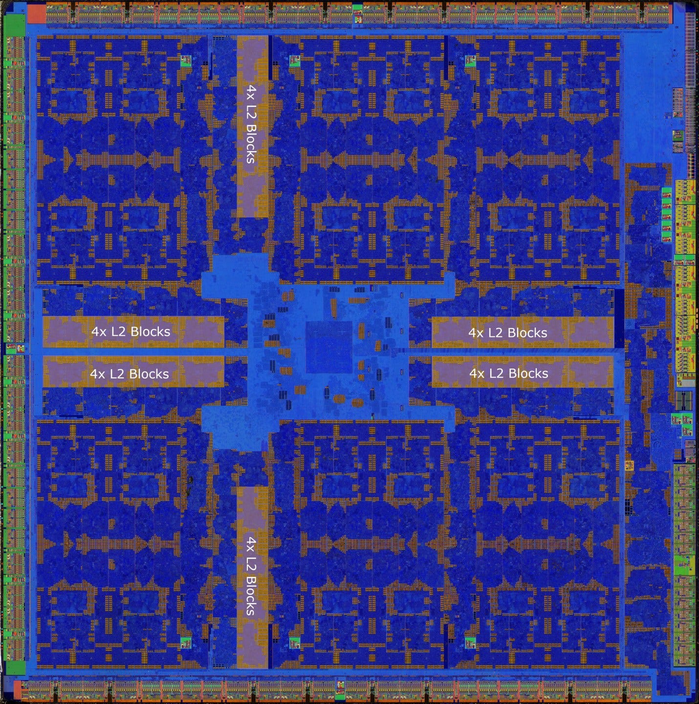
Maxwell enjoys doubled L2 capacity compared to Kepler. GM200 has 3 MB of L2 cache compared to GK210’s 1.5 MB. Visually inspecting the GM200 die shows 24 L2 blocks. Two L2 blocks likely form a slice attached to a memory controller partition, with 256 KB of capacity and 64 bytes per cycle of bandwidth.
GM200 should have 768 bytes per cycle of L2 bandwidth across the chip if Nvidia didn’t change the L2 slice arrangement from Kepler. At the EVGA GTX 980 Ti SC’s boost clock, that should be good for just over 1 TB/s of L2 bandwidth. AMD’s R9 390 has similar theoretical bandwidth. Unfortunately, Maxwell and Kepler struggle to make full use of available L2 bandwidth. AMD doesn’t have the same issue, so the R9 390 has a significant L2 bandwidth lead over the GTX 980 Ti.

Dividing by SM count and clock speed shows that per-SM bandwidth is below 32 bytes per cycle. Kepler’s SMs might be limited by a 32B/cycle interface. However Maxwell is not because I can get over 32B/cycle from L2 using a single OpenCL workgroup and global loads. That’s LD.E.128 and LDG.E.128 on Kepler and Maxwell respectively. Furthermore, L2 bandwidth isn’t limited by available parallelism. If we load SMs one at a time by increasing the workgroup count, the GTX 980 Ti’s bandwidth starts leveling off as we get past 17 or so workgroups. That suggests the L2 is running out of bandwidth and extra parallelism isn’t helping much.

However, Maxwell’s lower latency L2 makes bandwidth easier to utilize. The 980 Ti can still be at an advantage with draw calls for small objects, or in dealing with long-tailed behavior where a few threads take much longer to finish than others in the same dispatch.

L2 latency is higher on GCN, partially because its vector memory access path is high latency to begin with. Maxwell also benefits from an integer scaled add (ISCADD) instruction, which handles array addressing calculations for the low 32 bits of the address. GCN has to issue separate shift and add instructions.

GCN’s latency optimized scalar memory path sees just under 150 ns of L2 latency, putting it ahead of Maxwell. Thus AMD can have an advantage with memory accesses that the compiler can determine are constant across a wave.
Global Atomics
Because the L2 cache shared by the entire shader array, it’s a convenient place to handle global memory atomics. Maxwell, Kepler, and GCN’s L2 slices contain atomic ALUs to speed those operations up. Passing data between threads through global memory is definitely slower than doing so within a SM, but Maxwell still turns in a decent performance. It’s faster than Kepler, and quite a bit faster than GCN.

When looking at compiled assembly, Maxwell and Kepler both leverage ATOM.E.CAS instructions. AMD does the same with buffer_atomic_cmpswap. I find it funny that Kepler had fast atomics handling with global memory but not with shared memory.

Another funny Kepler trait is a cache invalidation instruction immediately after the atomic operation. I’m not sure why this is needed. Maxwell and AMD’s Hawaii both handle the atomic operation without requiring a separate cache control operation.
VRAM
Compared to other areas, Maxwell’s VRAM setup sees relatively little change compared to Kepler. Both architectures use GDDR5 setups with similar bus widths in the equivalent market segments. GM200 and GK210 both use 384-bit GDDR5 setups, while GK104 and GM204 use a 256-bit one. Maxwell benefits from slightly higher GDDR5 clocks, but most of the action is elsewhere. Instead of relying on huge bandwidth increases, Maxwell combines a larger L2 with tile based rasterization to reduce its dependence on VRAM bandwidth.

AMD took the opposite approach. The R9 390 uses a 512-bit GDDR5 bus running at lower clocks. Even though the R9 390 competes in a lower performance market segment than the GTX 980 Ti, it still achieves higher memory bandwidth. AMD’s Fury X competed directly with the GTX 980 Ti and used a 4096-bit HBM configuration. Both of those AMD products enjoy more VRAM bandwidth than the GTX 980 Ti, and will have an advantage if cache hitrates are low.
In turn, Nvidia has a latency advantage. The 980 Ti has better VRAM latency than the R9 390, meaning it needs less work in flight to hide that latency. AMD’s move to HBM gives Fury X a lot of bandwidth, but sharply regresses latency.

Part of AMD’s higher VRAM latency is again attributable to the higher latency vector memory path. GCN’s latency optimized scalar path turns in a better performance, but Hawaii is still behind GM200. Similarly, the Fury X continues to see even worse VRAM latency.

VRAM access of course includes time to check each level in the cache hierarchy. We can normalize for some of that by looking at how far (in time) VRAM is beyond L2. Sources of latency after the L2 has detected a miss would include the path from L2 to the memory controllers, any queueing delays in the memory controller, and finally the latency of the GDDR5 chips. With that metric, GM200 Maxwell with 7 GT/s GDDR5 is again similar to GK104 Kepler with 6 GT/s GDDR5. GK210 Kepler with 5 GT/s GDDR5 is a bit slower.
On AMD’s side, factoring out latency to L2 paints HBM in a slightly better light, as it’s now just 50 ns worse than GDDR5. Curiously, this aligns with CPU HBM latency characteristics. Fujitsu’s A64FX is documented to have 131-140 ns of latency with HBM2, while a typical desktop has 80-90 ns of latency to DDR4 or DDR5. So, DDR memory also has about 50 ns less latency than HBM. Of course some desktops have even lower latency thanks to XMP memory, but it’s important to not break rule 1 of the XMP club.

Maxwell’s VRAM upgrades are pretty unremarkable compared to changes in the rest of the architecture, but it’s still a step forward. Getting similar or better latency than Kepler while increasing VRAM capacity and bandwidth is a good generational improvement.
Maxwell’s Compute Performance
Maxwell may be optimized for consumer gaming, but its shader array help with compute too. Nvidia did cut back on FP64, but Maxwell is a strong contender if you don’t touch that.
VkFFT offers a Fast Fourier Transform implementation that can run on several different APIs. I’m using OpenCL here because the Tesla K80 can’t do Vulkan compute.

AMD’s GCN architecture continues to excel in this test, thanks to massive compute and memory bandwidth. The Kepler based Tesla K80 got demolished by AMD’s R9 390, but Maxwell gets a lot closer. With certain systems that look more compute bound, the GTX 980 Ti can pull off victories too.
Because VkFFT is prone to getting bandwidth bound, the test also prints out estimated memory bandwidth figures.

VkFFT gets as much bandwidth as a VRAM microbenchmark does on the R9 390. Maxwell could be held back by something else. Or maybe Maxwell doesn’t get along with the test’s access patterns as well as GCN does.
FluidX3D implements the Lattice Boltzman method for fluid simulations. The FP32 mode tends to be quite memory bandwidth bound too.

Despite having less theoretical bandwidth than the R9 390, the GTX 980 Ti pulls off a lead. It also turns in a much better performance than the Tesla K80.
Final Words
Maxwell was an exceptionally strong architectural overhaul. Nvidia was able to deliver a large generational performance increase without a new process node, and without a big jump in power consumption. Maxwell achieves this by aggressively focusing on gaming and cutting features that games didn’t utilize well. Configurable FP64 ratio, higher Shared Memory bandwidth for 64-bit types, and different caching paths for texture and data were dropped. Four texture caches and associated quad-TMUs were consolidated into two. Shared FP32 units were dropped. All of these changes helped reduce SM area and power, while allowing higher clocks.
Besides slimming down the SM, Nvidia made iterative improvements focused on keeping the execution units fed. Static scheduling was improved, latency for all sorts of operations came down, and L2 cache capacity increased. The resulting Maxwell SM was lean and mean, offering most of a Kepler SM’s performance by keeping its execution lanes well fed. Finally, Nvidia took it home by dramatically increasing the SM count in each market segment.
Maxwell’s improvements without a new process node are no doubt impressive, but they did come at a cost. Without decent FP64 capability, Nvidia couldn’t make a HPC Maxwell variant. Datacenter Maxwell cards like the Tesla M60 had competent compute credentials, but only if you stayed away from FP64. GK210 Kepler would have to hold the line in that arena until Nvidia came out with a true HPC replacement, and that didn’t come until P100 Pascal. But AMD wasn’t a significant competitor in that area, so it didn’t matter.
As a testament to Maxwell’s solid design, newer architectures like AMD’s RDNA(2) and Nvidia’s Ampere and Lovelace also divide their basic building blocks into four sets of 32-wide vector units. Nvidia continued to use Maxwell’s static scheduling control code format at least up through Turing3. Maxwell’s strategy of using more cache instead of bigger sophisticated VRAM configurations was repeated on AMD’s RDNA 2 and Nvidia’s Ada Lovelace, though with an order of magnitude larger last level caches. Perhaps Maxwell’s most impressive accomplishment was setting the stage for Pascal. Pascal uses a similar microarchitecture but clocks higher and implements more SMs thanks to a new process node. Despite being more than seven years old, Pascal GPUs are still listed within the top 10 spots on Steam’s November 2023 Hardware Survey. For any GPU architecture, that kind of longevity is incredible.
Nvidia’s strategy with Maxwell contrasts with AMD’s focus on scaling up GCN. Hawaii and Fiji had more Compute Units and larger memory buses. AMD also implemented more rasterizers and improved ACEs to feed the larger shader array. But the basic Compute Unit only received minor tweaks compared to the original GCN architecture that released just before Kepler. Nvidia’s ability to dramatically overhaul the SM in Maxwell set Nvidia up for massive success with Pascal and future generations.
If you like our articles and journalism, and you want to support us in our endeavors, then consider heading over to our Patreon or our PayPal if you want to toss a few bucks our way. If you would like to talk with the Chips and Cheese staff and the people behind the scenes, then consider joining our Discord.
References
Zhe Jia et al, Dissecting the NVidia Turing T4 GPU via Microbenchmarking
XiuXia Zhang et al, Understanding GPU Microarchitecture to Achieve Bare-Metal Performance Tuning
Ari B. Hayes et al, Decoding CUDA Binary