
Inside Qualcomm’s Adreno 530, a Small Mobile iGPU

GPU architectures vary drastically depending on their primary use cases. Mobile designs like Qualcomm’s Adreno face a daunting set of challenges, with smaller power and area budgets than even Intel’s iGPUs. Mobile SoCs have to share a small SoC die with a CPU, modem, DSP, ISP, and often a NPU. Within those constraints, Adreno has to drive games at screen resolutions rivaling that of desktop monitors. For example, the LG G6 has a 2880×1440 screen.
To get a grasp on how mobile GPUs tackle these challenges, I’ll be looking at Qualcomm’s Adreno 530 as implemented in the LG G6’s Snapdragon 821. Like recent AMD, Intel, and Nvidia GPUs, Adreno 530 has a unified shader array. DirectX 11.2, OpenGL 3.1+, Vulkan, and OpenCL are all supported. In theory, Adreno 530 can run a wide variety of games and even take on an occasional compute workload.

Unlike AMD and Nvidia GPUs, Qualcomm has published almost no information on their internal GPU architecture. Dissecting a GPU through software is far more difficult than doing so for a CPU, because there’s no way I’m writing assembly for individual GPUs for a free time project. I’m going to try my best with the OpenCL tests I’ve written over the past couple years, but there will be gaps and guesswork along the way.
System Level
Like other GPUs, Adreno 530 gets work when the CPU writes commands into its ring buffer. Adreno’s Command Processor (CP) consumes these commands and generates work for the shader array.
Adreno 530’s shader array consists of four Shader Processors (SPs). Each SP has a private scheduler feeding a set of execution units, along with texture units and a small texture cache.

The entire shader array along with various fixed function units share a 128 KB L2 cache. For memory access, the iGPU shares a LPDDR4 subsystem along with everything else on the Snapdragon 821 SoC. Adreno 530 can use up to 1.8 GB of the LG G6’s 4 GB of RAM, but maximum size for individual allocations is limited to 472 MB.
Adreno 530 clocks up to 653 MHz on the Snapdragon 821. Its shader array can achieve a modest 334 GFLOPS at that speed, making it somewhat weaker than Intel’s ubiquitous Gen 9 GT2 iGPUs.
Similarities to AMD Radeon
Internally, Adreno’s CP consists of a Microcode Engine (ME) and a Prefetch Parser (PFP), which curiously match naming conventions on AMD GPUs. As with an AMD GPU, the driver loads both PFP and ME firmware as part of initializing the device3. And as with AMD GPUs, the ME firmware is also referred to as PM4 firmware.
This is likely due to Adreno’s IP being based on the Imageon IP that was sold to Qualcomm by AMD back in 2009. So Adreno and Radeon sharing the same lineage likely explains the similar naming conventions between the two lineups.
PM4 is AMD Radeon’s command packet format. Source code shows similarities between Adreno and Radeon’s PM4 formats, but they’re not identical. Both Radeon and Adreno specify packet types 0 through 3 via the two highest bits of the 32-bit packet header. However, Adreno extends the packet type field by another two bits to support type 4 and type 7 packets.
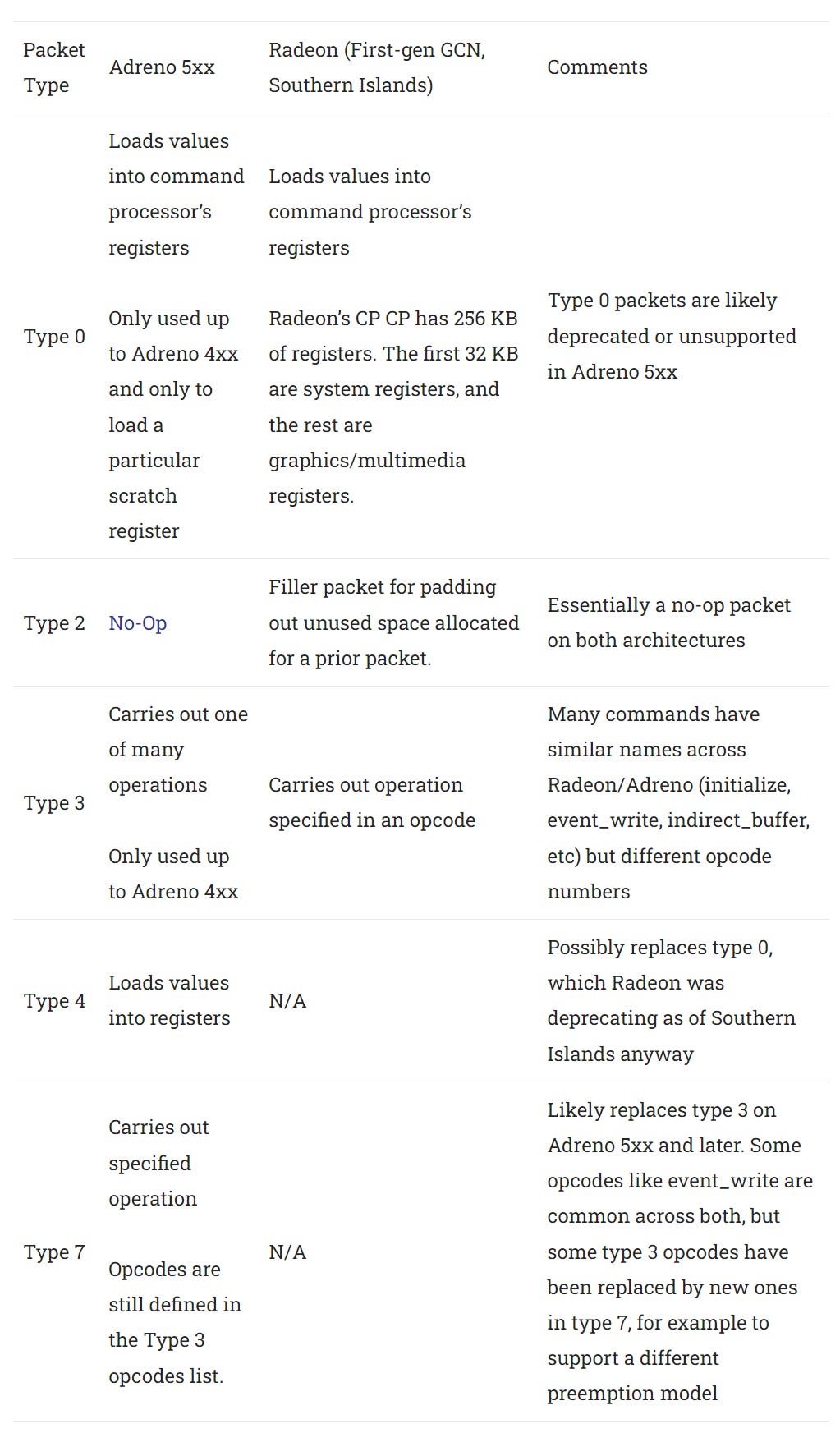
Adreno’s command processor likely started with some Radeon DNA, but by Adreno 530, the two command formats have diverged. As part of GCN’s move towards compute, AMD’s command processor got the ability to manage multiple ring buffers (specifically, two compute queues in addition to the primary graphics one) whereas Adreno 5xx went in a different direction with a new preemption model.
Preemption refers to interrupting work in progress, saving state, and switching to another task. Type 4 packets can define memory ranges for the CP to save state when preempted. But eventually Adreno would get multiple queues too. Also, Radeon’s preemption subjectively feels snappier than Adreno’s. I often see the cell phone’s screen freeze when running compute tasks on Adreno 530, but not on GCN GPUs.
Adreno 530’s Shader Processor
Adreno 530’s SP has 64 FP32 lanes along with a vector register file of unknown size and scheduling hardware. Special functions like reciprocals and inverse square roots execute at 1/8 rate, in line with Nvidia’s Ampere architecture. Intel’s Gen 9, AMD’s GCN, and Nvidia’s Maxwell however place more emphasis on special function units, and handle those at 1/4 rate. Qualcomm executes integer multiplies at 1/4 rate, in line with Maxwell and GCN.

Adreno places particularly low importance on 64-bit data types. INT64 adds execute at quarter rate. Desktop GPUs typically handle 64-bit adds with a pair of add-with-carry operations, resulting in half rate throughput. However, low INT64 performance is a trait shared with Intel’s Gen9 architecture. FP64 support is completely absent from Adreno, as mobile GPUs have no place taking on high performance compute.

Adreno instead focuses on lower precision types. Like Nintendo Switch’s special Maxwell implementation, FP16 operations execute at double rate. With fused multiply-add FP16 operations, Adreno 530 can achieve just over 540 GFLOPS, providing a notable advantage over Intel’s architecture. Of course, developers have to optimize their code to get by with lower precision in order to see that advantage. 16-bit integer operations also benefit, with INT16 multiplies enjoying full rate execution. On AMD’s GCN, there’s no advantage to using INT16 over INT32.
Wave Size and Scheduling
Note: I (Clam) originally thought Adreno 530 used wave64 execution based on Mesa code and per-workgroup throughput. After further experimentation, my previous conclusion was flawed. Divergence penalties are a better way of determining wave width because per-workgroup throughput only shows ALU count in a SP.
Wave size refers to vector width on a GPU. GPUs achieve high throughput at low power by using wide vector execution. GCN for example uses 64-wide waves, so one vector instruction applies the same operation across 64 32-bit elements. That means the GPU only has to pay the cost of fetching, decoding, and tracking an instruction through the pipeline once for 64 math operations. However, applying the same operation across the entire wave means wider waves are more prone to losing throughput if control flow diverges.
Intel’s Gen 9 architecture uses flexible wave sizes going up to 32, while Nvidia has used 32 wide waves since the beginning of (unified shader) time. I believe Adreno 530 uses 32-wide waves based on divergence penalties.

Qualcomm1 states that wave size can vary across Adreno GPUs. Adreno might be using different SP widths for more configuration flexibility. For example, a smaller Adreno GPU could use SPs with 32 FP32 lanes operating in wave32 mode. AMD’s old Terascale used a similar scheme, where a nominally 80 (16×5) lane SIMD with wave64 execution could be cut down to 40 (8×5) lanes with no changes to the scheduling algorithm. A hypothetical 32-wide SP with wave64 in contrast would need a new scheduler that understands it can’t issue wave64 instructions back to back, as doing so would oversubscribe the execution units. Keeping the architecture as similar as possible across different products helps reduce engineering costs.
Wave size depends on Adreno GPU series and tiers as well as the compiler; values could be 8, 16, 32, 64, 128, etc.
Qualcomm Snapdragon Mobile Platform OpenCL General Programming and Optimization
Besides using wide vectors, GPUs hide latency with thread level parallelism. GCN for example can track 10 threads in each of a Compute Unit’s four SIMDs. I’m talking about CPU-like threads here, where each thread has an independent instruction pointer. Since each thread’s instructions can operate on a 64-wide vector, a GCN SIMD can have 640 32-bit operations in flight.
Qualcomm did not directly document a SP’s scheduler size, but Adreno 530’s SPs have a peculiar limitation of one workgroup in flight. That limitation can be nasty if workgroup sizes are small, and isn’t a limitation shared by any Intel, Nvidia, or AMD architecture as far as I know. But for analysis purposes, it’s useful because it implies a SP’s scheduler capacity. Adreno 530’s maximum OpenCL workgroup size is 1024, or 32 wave64 threads. Thus an Adreno 530 SP likely has 32 scheduler entries. Freedreno code in Mesa backs this up.

The SP’s scheduler appears split into two scheduling partitions, with waves assigned in a round-robin fashion. Best throughput will be achieved when workloads are evenly split across the two partitions.
SP Caches and Local Storage
Parallel processors like GPUs can demand high bandwidth from their memory subsystems. Adreno 530 is a small GPU, with a memory subsystem that looks tuned for low power and area rather than high performance.

Local Memory
A GPU’s fast memory after registers is often a small software managed scratchpad. Unlike a cache, software has to explicitly load data into the scratchpad. Once it does so, it can enjoy consistently low latency and high bandwidth to that data. OpenCL exposes this fast storage through the local memory space. Adreno 530 lets kernels allocate up to 32 KB of local memory and can only track one workgroup per SP, so each SP almost certainly has just 32 KB of local memory.
Nvidia calls their backing structure for local memory “Shared Memory”. AMD calls it the “Local Data Share” (LDS), while Intel calls it “Shared Local Memory” (SLM). I don’t know if Qualcomm has a special term of their own.

Adreno 530 enjoys good local memory latency, especially considering its low clocks. It’s much better than Intel’s Gen 9 architecture, which implements its SLM with 64 KB of storage in the L3 banks instead of making it local to each Subslice (an Intel iGPU subdivision analogous to a SP). AMD’s GCN architecture has very poor local memory latency when running at just 680 MHz in the FirePro W2100. Likely, AMD designed GCN with much higher clock speeds in mind.
Bandwidth however is less impressive on Qualcomm’s GPU. Each SP seems to cap out at just under 32 bytes per cycle of local memory bandwidth, or half what an Intel Gen 9 Subslice can do per cycle. I achieved the best bandwidth figures using a float4 version of my local bandwidth test, which provides more instruction level parallelism. Adreno 530 was able to launch my float4 version with a workgroup size of 256, meaning each SP basically had four SMT threads active (assuming wave64). The scalar and 64-bit versions of the bandwidth test could launch with a workgroup size of 512, but Adreno seems to prefer more instruction level parallelism over thread level parallelism.

With just under 80 GB/s of local memory bandwidth, Adreno 530 has similar load bandwidth to the quad core Kryo CPU it shares a die with. Intel’s Gen 9 GT2 GPU enjoys more than twice as much local memory bandwidth, though it’s not much in absolute terms either. A single Skylake core on the i5-6600K can pull over 220 GB/s from L1 for perspective.
Besides being a fast software managed scratchpad for frequently used data, local memory can be used to exchange data between threads in the same workgroup. Thread-to-thread latency when bounding a value between threads is only slightly worse than pointer chasing latency, suggesting Adreno has fast integer atomic units built into its local memory block.

Intel and AMD see higher latency in this test. AMD’s Oland chip in the FirePro W2100 has a particularly poor time.
Texture Cache
For actual hardware managed caching, each SP has a 1 KB read-only texture cache. Originally I didn’t think a SP had any private caches, but Freedreno says Adreno 330 has a 1 KB texture cache. I added a 1 KB test size to my texture cache latency test, and well, it’s there. I don’t understand the point of a 1 KB cache, but apparently Qualcomm does because they’ve kept it for multiple generations.
Unlike GCN’s general purpose L1 vector cache, Adreno’s L1 is read-only and only caches image objects. OpenCL’s image1d_buffer_t can be cached in that L1, but general global memory accesses are not.

Texture cache latency is somewhat higher than that of local memory, which is expected because caches require tag and state checks with every access. The texture cache is also tied to the texture units, which aren’t latency optimized. But latency compares well against Intel’s Gen 9 and AMD’s GCN. As with local memory, Adreno makes up for low clocks by having a shorter cache access pipeline.
Segmenting the test array between multiple workgroups shows the 1 KB texture cache is private to each SP. A 1 KB test size with four workgroups would mean each workgroup traverses a 256 byte portion of the test array. Testing with higher workgroup counts dramatically increases measured latency as not all workgroups will be able to launch in parallel.

Adreno 530 thus has 4 KB of texture cache capacity across its shader array. Bandwidth from the texture caches is decent and about the same as local memory bandwidth. Adreno isn’t far behind Intel’s HD 530.

AMD’s GCN is a cache bandwidth monster and Oland is no exception. With five Compute Units each capable of loading 64 bytes per cycle from L1, Oland can still deliver a lot of bandwidth even at 680 MHz. But stepping back, none of these GPUs have a lot of cache bandwidth on tap. A Phenom II X4 945 from the late 2000s has 350 GB/s of L1 bandwidth across its four cores, and can pull over 90 GB/s from its much larger L2 caches.
L2 Cache
Because Adreno’s L1 is a specialized read-only texture cache, Qualcomm decided not to use it for general compute accesses. Those bypass L1 and go directly to the GPU-wide 128 KB L2. Qualcomm calls this the UCHE in drivers, which likely stands for Unified Cache. Unlike the L1, the L2 can handle writes and make them visible across the entire shader array.

From the texture path, L1 misses can be serviced by L2 with just over 122 ns of total latency. Again this compares well to Intel, where the HD 530’s shared cache sees 175 ns of latency. And GCN suffers from high latency especially at low clocks.

Directly hitting the L2 with global memory accesses shows better latency characteristics. Adreno 530 looks a lot like the HD 530 here. Both have compute accesses bypass L1 and rely on the GPU-wide shared cache to service them. Such a strategy makes sense for small iGPUs where compute and cache can be placed close together on a small, low latency interconnect. Large GPUs don’t have this luxury. For example, the GTX 980 Ti’s 3 MB L2 cache has over 180 ns of latency.

In a consistent trend, Adreno 530 doesn’t have a lot of L2 bandwidth. I measured about 40 GB/s, or half of L1 bandwidth. GCN and HD 530 both enjoy better bandwidth from their GPU-wide shared caches, and by a significant margin.

Testing with different workgroup counts also shows how Adreno’s one workgroup per SP limitation can make high bandwidth difficult to achieve. Bandwidth tends to be lower when workgroup count is not a multiple of SP count. I ran the test up with up to 24 workgroups on both HD 530 and Adreno 530. While Intel’s HD 530 sees slightly better bandwidth when workgroup count is a multiple of 3 (the Subslice count), the effect is nowhere near as pronounced as it is on Adreno.
VRAM Access
As an integrated GPU, Adreno 530 shares a memory controller with the CPU and other SoC components. I’m not sure what memory LG paired the Snapdragon 821 with in the G6, but Techspot says the G5 had 29.8 GB/s of theoretical bandwidth with its similar Snapdragon 820 chip.

I don’t get close to that with a bandwidth test. Instead, I see 14-15 GB/s, which is in line with what I measured from the CPU side. Adreno 530 doesn’t have a lot of bandwidth to work with. Small caches on both the CPU and GPU side could put a lot of pressure on the memory controller.
Adreno enjoys relatively good memory latency for a GPU at just over 266 ns, assuming you stay within 16 MB. But past that, Adreno might be suffering from TLB miss penalties. If so, TLB fills are extremely expensive, and Adreno 530 has over 500 ns of latency at the 256 MB test size. Intel’s HD 530 has more consistent latency when accessing system memory, at just over 330 ns. That likely includes TLB miss penalties because Intel documents a 768 entry TLB.

AMD’s FirePro W2100 suffers from much higher VRAM latency. Much of that is down to high cache access latency due to low clocks.
CPU to GPU Link Performance
Integrated GPUs often enjoy faster data movement between CPU and GPU memory spaces than their discrete counterparts. Because both the CPU and GPU share the same memory controller and physical memory pool, copy speeds aren’t limited by PCIe bandwidth.
Adreno 530 turns in a decent performance, particularly when copying data into the GPU’s memory. However, copying in the other direction results in very low bandwidth. I suspect that’s because games rarely have to move data from the GPU to the CPU. Textures, geometry, and commands have to be sent from the CPU to the GPU. The GPU renders outputs to the screen, after which they are discarded (unless the user takes a screenshot).

Intel’s HD 530 shows what an iGPU setup can achieve. Both the iGPU and CPU share a 6 MB last level cache on the Core i5-6600K, letting small transfers stay on-die. Bandwidth is still good for larger copies thanks to the relatively high bandwidth 128-bit DDR4-2133 memory configuration, but Adreno 530 does pull ahead. Both integrated GPUs clobber the FirePro W2100, which only has a x8 PCIe 3.0 link.
Compute Performance: FluidX3D
Adreno 530’s graphics performance is well documented by sites like Techspot, so I’ll take a look at compute performance. FluidX3D uses the lattice Boltzmann method to simulate fluid behavior. It features special optimizations that lets it use FP32 and still deliver accurate results in “all but extreme edge cases”.
While FluidX3D uses OpenCL and can run just about anywhere, it’s written with powerful desktop and datacenter GPUs in mind. To fit within the Adreno 530’s constraints, I’m running a smaller version of the built in benchmark with a 128x128x128 grid resolution. The default benchmark uses a 256x256x256 grid, which exceeds Adreno 530’s limit for a single allocation. I also had to make FluidX3D print update speed in thousands of lattice cell updates per second, rather than millions. Otherwise, the benchmark says Adreno 530 achieves 0 MLUPs/s. Qualcomm was able to achieve of a level of performance that FluidX3D’s author did not account for, though not in a good way.

Adreno 530 performs very poorly. Because LBM is often memory bound, FluidX3D has FP16S and FP16C modes that store data in 16-bit FP formats. Since FP16 is only used for storage (math is still done in FP32) and extra operations are required for format conversion, those modes serve to use more compute power to reduce memory bandwidth demands.
The FirePro W2100 and HD 530 both benefit from FP16 storage, but Adreno 530 does not. Adreno 530 is likely compute bound, and is held back by shader array inefficiencies rather than memory bandwidth.
Final Words
Different performance and power targets demand different designs, and Adreno 530 is an excellent example. Mobile GPUs have to drive high resolution screens and support gaming while fitting within a very tight power and area budget. Qualcomm tackles these challenges with a different architecture strategy than what we see in AMD and Nvidia GPUs, and even Intel iGPUs. They run a relatively wide shader array at low clocks, have small caches, and accept limitations like 1 workgroup per SP that wouldn’t fly on more general purpose GPUs.

Like Nvidia’s custom Maxwell implementation in Tegra X1, Adreno 530 compensates for low bandwidth and small caches with an emphasis on FP16 performance. Its SPs can execute basic FP16 operations at double rate, and FP16 values make more efficient use of storage and bandwidth.
However, some design choices baffle me. I can’t understand how 1 KB texture caches makes sense. Even Terascale from before 2010 gave each SIMD a 8 KB L1 texture cache. Perhaps mobile GPUs expect very small, low resolution textures. But Apple’s M1 also has a 8 KB first level cache, and serves in mobile designs too. But I guess Qualcomm knows what they’re doing. Because in the end, Adreno 530 delivered competitive graphics performance. Techspot has it near the top of the chart on offscreen tests, which factor out differing screen resolutions.
If you like our articles and journalism, and you want to support us in our endeavors, then consider heading over to our Patreon or our PayPal if you want to toss a few bucks our way. If you would like to talk with the Chips and Cheese staff and the people behind the scenes, then consider joining our Discord.
References
Qualcomm Snapdragon Mobile Platform OpenCL General Programming and Optimization
In-tree Adreno drivers, https://github.com/torvalds/linux/blob/0dd3ee31125508cd67f7e7172247f05b7fd1753a/drivers/gpu/drm/msm/adreno/a5xx_gpu.c#L570