
Kryo: Qualcomm’s Last In-House Mobile Core

CPU design is hard. You can tell because there aren’t a lot of companies doing it. AMD and Intel are your only choices in the PC scene. In the Android ecosystem, ARM Ltd’s cores dominate. Qualcomm, MediaTek, Samsung and other SoC makers put chips together with varying core counts, GPUs, and other IP blocks. The architecture in all of their CPU cores today, however, comes from ARM the company. If it’s not directly branded as ARM Cortex, you can bet it’s a customized version of an ARM Cortex core. But things weren’t always that way. Samsung used to make their own “Mongoose” cores up to 2019. Qualcomm did the same up to 2016 with the Kryo architecture.
Kryo is special. It would be Qualcomm’s first and last 64-bit mobile ARM core. It would also be Qualcomm’s first and only shot at creating an in-house hybrid core designs. Among hybrid core designs, it’s also unique in using the same microarchitecture in both “big” and “little” clusters, with different clock speeds and cache configurations.

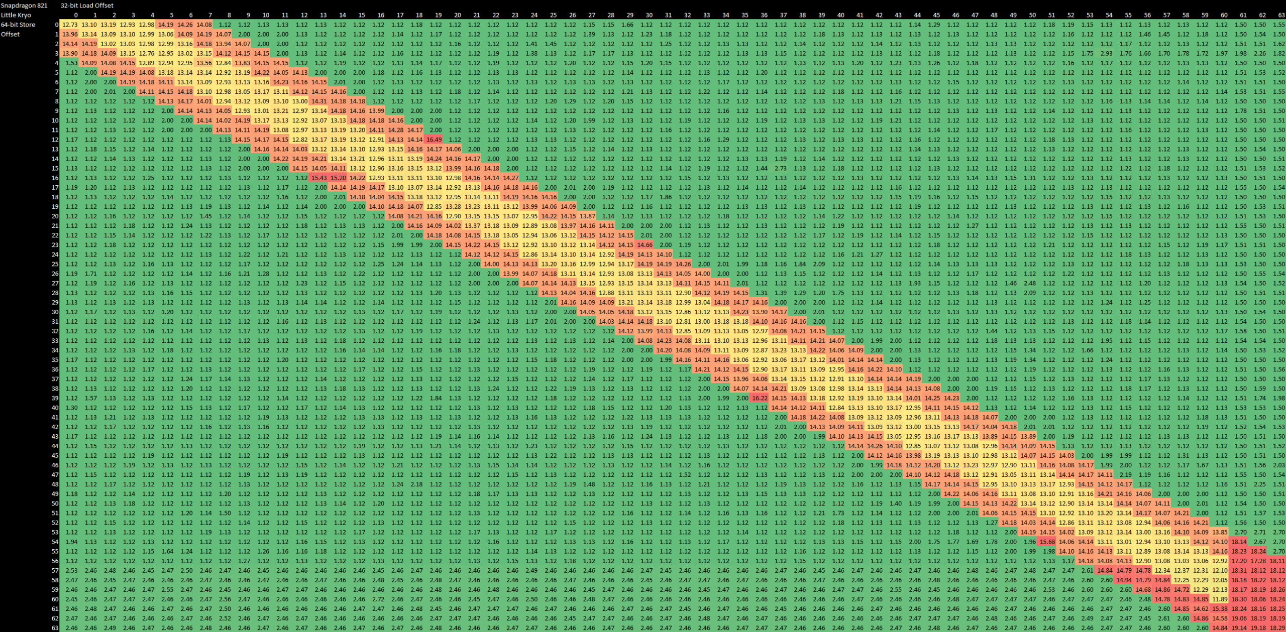
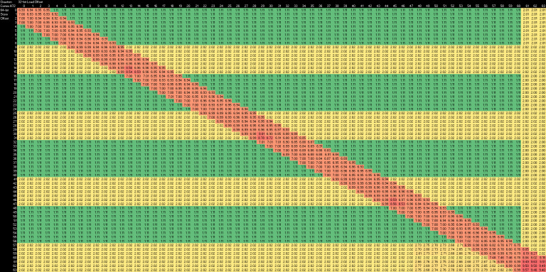
lscpu output for Kryo, showing the two clusters. Little cores rarely clock to their maximum 2.18 GHz, and instead tend to hang out around 1.58 GHz under load.Kryo debuted in the Snapdragon 820. There, it succeeded the badly received Snapdragon 810. In Qualcomm’s CPU history, Kryo comes after a line of venerable in-house 32-bit ARM cores like Scorpion and Krait. Here, we’re testing Kryo in the Snapdragon 821, as implemented in the LG G6. Because the phone is running Android, testing is an absolute nightmare because of system noise. On top of that, memory latency can’t be tested with huge pages because Android doesn’t support that. I’m trying my best here, but please take the test result with a grain of salt.
Block Diagram
Kryo is an aggressive design for a 2016 mobile core. It’s a 4-wide out-of-order architecture with substantial reordering capacity and ample execution resources. ARM’s cores around that time include the 3-wide Cortex-A72 and 2-wide Cortex-A73. Core width says little about performance, but A72 and A73 are less ambitious than Kryo in most respects.

Frontend: Branch Predictor
A CPU’s branch predictor sits at the start of the pipeline, and is responsible for steering the CPU in the right direction. Going down the wrong path means wasted work, and wasted work means lost performance and wasted power. CPU designers have to strike a balance though, because a more sophisticated branch predictor will cost more power and area. Kryo gets modest branch prediction capabilities.

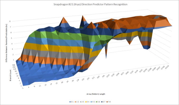
It can recognize patterns about as well as Cortex-A72, but doesn’t do well when a lot of branches are in play. It’s far less capable than Skylake, which is expected for a low power core.
Branch Target Caching
Speed is important for a branch predictor too. A program will typically have a branch about every ten instructions. Stalling for less time after a taken branch is a good thing. High performance CPUs like Intel’s Skylake attack this problem with a very large, very fast cache of branch targets. Kryo, however, has a different set of design parameters. It’s not meant to handle heavy lifting the way desktop CPUs do, so it doesn’t have to clock very high. Because it goes into a mobile SoC, core area and power take precedence over absolute performance. With that in mind, it looks like Kryo’s designers opted for a conservative approach to branch target caching.
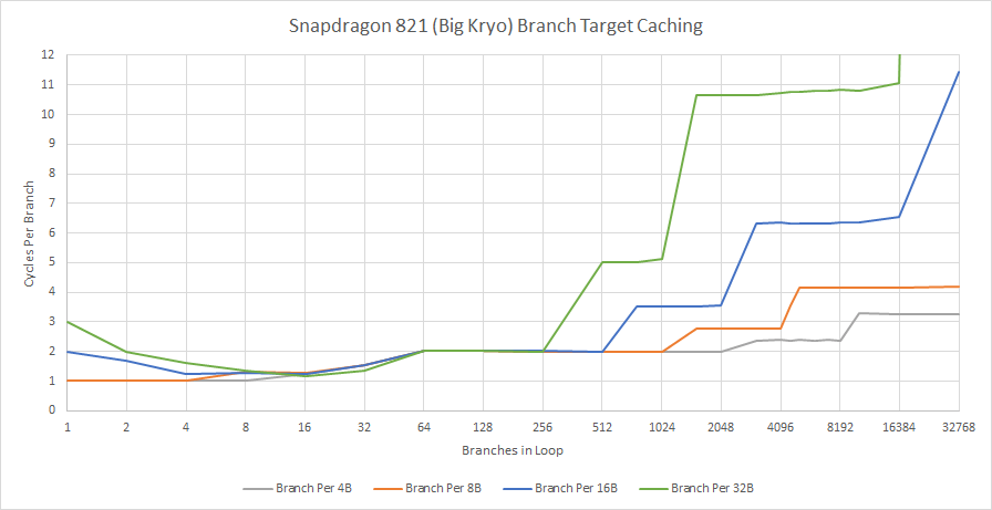
For tiny loops, an 8-entry branch target buffer (BTB) can handle branches back to back. After all, there might not be another BTB. Instead, Qualcomm might be using a fast branch address calculator alongside a L0 + L1 instruction caching setup. Krait used a L0 instruction cache, so there’s precedent within Qualcomm for such an approach. If so, we’d be looking at a 8 KB L0 cache with 2-cycle latency. Past 8 KB, branch penalty varies, but is generally within the cycle counts we’d expect for a last-level BTB hit. For example, AMD’s Piledriver and Zen 2 suffer 5-cycle latency when using their L2 BTBs.
Branch predictor cannot effectively drive instruction prefetching, because taken branch latency increases dramatically as the test exceeds L1 instruction cache (L1i) capacity. Exceeding L2 capacity is painful. The largest test size with a branch every 32 bytes and 32768 branches has a 1 MB instruction footprint, and wound up taking nearly 100 cycles per branch. For the sake of morale, I’ve adjusted the graph not to show this.
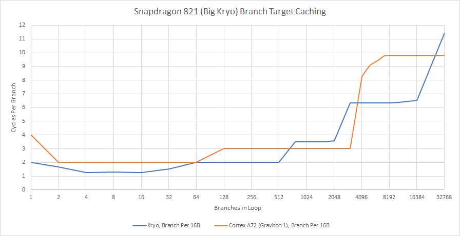
Kryo turns in a good showing next to ARM’s Cortex-A72, especially for small code footprints. ARM’s contemporary architecture cannot handle back-to-back taken branches at all. Cortex-A72 is slower when using its main BTB than when Kryo fetches branches from its L0 and calculates targets on the fly. Past 8 KB, differences start to even out.
Indirect Branch Prediction
Programmers are fond of using lower performance languages and coding patterns to piss off CPU architects. Object-oriented languages use vtables to associate method code with objects. That often means one branch can go to several different targets (i.e., an indirect branch) depending on the programmer’s level of object disorientation. Similarly, switch-case statements can also be compiled into an indirect branch. As a coping mechanism, CPU architects have implemented indirect branch predictors. Indirect predictors track multiple targets per branch, and choose between them typically according to global history.
Kryo’s indirect predictor is reasonably capable for a low power implementation. It can cope with 16 targets for a single branch, or up to 64 total targets if each indirect branch only cycles between two targets.
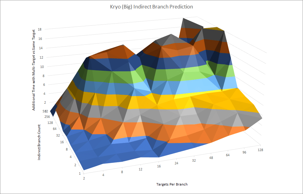
ARM’s Cortex-A72 has similar coping capabilities for a single troublesome indirect branch, but can cope a bit better when there are a lot of indirect branches. In testing, it had reasonably low penalties out to 128 branches, with two targets each.
Return Prediction
Return is a special case of indirect branches because it’s used to return from function calls. That usually means they line up with a preceding call, making prediction easy. The branch predictor can simply maintain a stack of return addresses, push to it whenever there’s a call, and pop off an address to predict a return.

Kryo has a 16-entry return stack, which should be deep enough for most cases. Intel architectures going back to Core 2 also had a 16-entry return stack. Cortex-A72 has a substantially deeper return stack, hinting at different optimization priorities.
Frontend: Instruction Fetch
Once the branch predictor has determined where to go, the frontend has to fetch instructions and feed them to the rest of the pipeline. Kryo uses a 32 KB L1i to speed this up. From the L1i, Kryo can fetch and decode up to four instructions per cycle. ARM’s Cortex-A72 has a three-wide frontend fed by a larger 48 KB L1i. The Cortex-A73 used on the next generation of Snapdragon SoCs only has a 2-wide decoder, so Kryo’s frontend is quite wide for a mobile core of its time.

If Kryo has to fetch code from L2, frontend throughput takes a sharp drop to just under 1 IPC. This is quite common for low power cores. Older desktop cores also struggle to keep up frontend bandwidth after a L1i miss, so this weakness is understandable. Kryo only loses significantly when compared to high performance desktop and server architectures from just a few years before it launched.
Rename and Allocate
A CPU’s renamer takes micro-ops from the frontend and allocates resources to track them in the backend. This stage typically does register renaming, helping to break false write-after-write dependencies and expose more instruction level parallelism to the backend. Because the renamer basically does an extra level of translation by mapping architectural, program-visible registers to internal entries in a physical register file, it’s also a convenient place to pull other tricks.
Kryo doesn’t do anything besides good old register renaming. There’s no special zeroing idiom recognition. However, that’s not a big problem for Kryo, because ARM instructions are always four bytes. On x86 CPUs, zeroing a register by xor-ing it with itself or subtracting it from itself would give you a smaller instruction footprint, because register to register math instructions could be encoded in two or three bytes (versus five or more bytes for a move-immediate instruction). Move elimination is also absent on Kryo, but I really can’t hold this against Qualcomm because ARM didn’t figure this out until a few generations later.
Out of Order Execution
Out of order execution is essential to high performance, because it lets CPUs move past long latency instructions and attempt to hide that latency by finding other independent instructions. Long long ago, out of order execution was purely in the realm of high power devices, because it needs large buffers to track in-flight instructions and very timing-critical structures like schedulers. However, advances in process technology have made out of order execution feasible within a cell phone sized power budget. Kryo is implemented on Samsung’s 14nm FinFET process, which is modern enough to let it implement a reasonably sized out of order execution engine.
Kryo offers similar maximum reordering capacity to ARM’s Cortex A72, but deals with other out of order buffers very differently. Qualcomm’s core looks very strong for branch-heavy integer code, while A72 places more emphasis on scalar floating point stuff.

Kryo can reach maximum reordering capacity even when about half the instructions in flight are branches. A large flags register file helps support that because conditional branches are often accompanied by flag-setting instructions. Kryo’s integer register file also offers more capacity, making backend stalls less likely with integer-heavy code.
ARM’s design is stronger for scalar floating point code, though it loses that advantage with 128-bit vector code because Kryo has full width vector registers. Memory ordering queues are small on both architectures, but A72 seems to be ahead here thanks to a much larger load queue. Kryo has a slightly larger store queue though, which could even things out because the store queue tends to be very hot structure.
Schedulers are also very hot structures because they track instructions that are waiting on unsatisfied dependencies. Implementing large schedulers is difficult because they have to check every entry, every cycle to see if there’s something ready to execute. Kryo generally enjoys better scheduler capacity than Cortex A72.

Cortex A72 uses a distributed scheduler layout with small, single-ported queues. Kryo’s scheduler is mostly distributed, but not completely. The integer scheduler uses two dual-port queues, which provides similar total scheduling capacity to ARM’s four distributed queues, but allows those entries to be used more flexibly. Kryo uses distributed queues for floating point and memory scheduling, but those queues are larger than ARM’s. Overall, Kryo’s scheduler is a lot better than A72’s, and probably more expensive in terms of power and area too.
Integer Execution Units
Kryo has an exceptionally strong set of integer execution units. With four ALUs, it has as much per-cycle throughput for basic integer operations as desktop CPUs. Skylake can handle two branches per cycle provided at least one is not-taken, giving it better branch throughput than Kryo. In exchange, Kryo enjoys superior integer multiplication throughput. It’s not a particularly good tradeoff, especially because Kryo has 5 cycle multiplication latency compared to 3 cycles on Skylake.
But compared to any mobile core, there’s not much to complain about. Cortex A72 also has 5 cycle multiplication latency, and only one port available for integer multiplies. With just two ALUs, port contention is more likely on A72 too.
Floating Point and Vector Execution
Low power CPUs typically can’t afford high floating point throughput the way desktop and server CPUs can. Wide execution units cost power and area, and cell phone SoCs aren’t exactly the place to run scientific simulations. But mobile CPUs can’t drop the ball on floating point performance. In order to maximize programmer confusion and hardware design frustration, Javascript’s basic “number” type is floating point. Javascript also features on just about every web page, making it important.
Therefore, Kryo and A72 both do quite well on scalar floating point performance. Kryo has two relatively fast 3-cycle FP adders, while Cortex A72 has slightly slower ones that take four cycles to generate a result. Vector FP performance is mediocre on both cores, but Kryo theoretically has more throughput because a 128-bit fused multiply add only occupies one FP pipe. That lets you dual issue a 128-bit packed FP add alongside a 128-bit FMA, giving 12 FP operations per cycle. Kryo also has better FMA latency at 5 cycles, while ARM takes a very ugly 7 cycles to complete the same operation.

Compared to Cortex A72, Kryo has far better vector integer execution. Vector INT32 adds complete with single cycle latency, while Cortex A73 has a three cycle pipeline for the same operation. Vector INT32 multiplication is pipelined over four cycles on both architectures, but Kryo has twice the throughput.
Vector operations are also useful for speeding up memory access, and Kryo is superior there too. It can do two 128-bit vector loads per cycle, though not consistently. That’s better than A72, which is limited to one load per cycle. When writing data, Kryo can complete a 128-bit store every cycle. Cortex A72 can only complete a 128-bit store every two cycles.
Load/Store Unit
Instructions that read from or write to memory go down an address generation port. Kryo has powerful address generation units that can handle indexed, scaled accesses with 3 cycle latency. After calculating virtual addresses, the load/store unit has to translate them to physical addresses and make sure memory accesses appear to happen in program order.
Kryo’s ability to find store forwarding opportunities is quite sophisticated. Like Skylake, it can forward store data as long as a dependent load is completely contained within a prior store. Curiously, it also appears to do a fast early dependency check on a 4-byte boundary. Unlike Skylake, it does fail when accesses cross a 64-byte cacheline boundary, but overall it’s quite a good performance for a mobile CPU.
Unfortunately, forwarding latency is terrible at 13 cycles. It’s nearly as bad as the 14-15 cycle failed forwarding case. It’s also as bad as Bulldozer on a cycle count basis, which is terrible because Kryo doesn’t clock high. Strangely, forwarding performance is a bit better on the FP/vector side. Data from a 128-bit store can be forwarded to an aligned 64-bit FP load with 10 cycle latency, or 11 cycles for a partial overlap. Misaligned vector loads take an additional cycle to forward.
In contrast, Cortex A72 handles memory dependencies well. Forwarding generally happens with 7 cycle latency. Even the most expensive cacheline crossing cases on A72 are faster than the “happy path” on Kryo.
Address Translation
Program-visible virtual addresses have to be translated to physical memory addresses. Operating systems maintain tables that map pages in virtual memory to ones in physical memory, but traversing those tables would require several memory accesses to service each memory access instruction. Obviously that’s unacceptable, so CPUs cache address translations in translation lookaside buffers (TLBs).
A lot of CPUs have multi-level TLBs. Kryo does not. In an all-or-nothing move, Kryo has a big and fast 192 entry L1 TLB and nothing after it. That can give Kryo a real advantage with small data footprints. But accesses in the mutli-megabyte range are going to be painful.
Cache and Memory Access
DRAM performance keeps falling farther and farther behind CPU performance, so good caching is critical to making sure DRAM performance doesn’t hold the CPU back too much. Kryo has a simple, two-level cache hierarchy that looks like something out of the mid-2000s. The L1D is a bit small at 24 KB, but enjoys 3 cycle latency.

After the L1, Kryo has a per-cluster L2 cache. Cores in the Snapdragon 821’s big cluster have a 768 KB (?) L2 cache with 25 cycle latency, while ones in the little cluster have a 512 KB L2 with 23 cycle latency. L2 latency is poor considering the low cache capacity. For comparison, Skylake’s 256 KB L2 has 12 cycle latency. In actual time, big Kryo has 10.9 ns of L2 latency, putting it into the same ballpark as Intel’s much larger L3 caches. Graviton 1’s A72 cores take 21 cycles to access a shared 1 MB L2, so each A72 core can access more cache and can get to it a bit faster.

Kryo does a tiny bit better in the bandwidth department. Its L1 data cache can handle two 128-bit vector loads per cycle. It can’t do so consistently, but A72 can never sustain more than one load per cycle, so Kryo gets an advantage.
From a single core, A72 and Kryo both have mediocre L2 bandwidth at just above 8 bytes per cycle. However, Kryo’s more distributed L2 design gives it better bandwidth scaling than Cortex A72. With a private L2 cache for each cluster, each cache instance only has to arbitrate between two clients, not four. ARM’s L2 might provide a lot of efficiently used capacity, but bandwidth stops scaling after two cores.

As a result, Kryo gets a substantial multithreaded bandwidth advantage, as long as you stay within L2. But that’s not a very big advantage in my opinion. L2 capacity is still a sore point. 512 KB or 256 KB caches are more suited to be mid-level caches, not a last level one. The L2 bandwidth advantage also drops under long running loads as the cores clock down to keep temperatures in check.

Accesses that miss L2 go straight to DRAM. The Snapdragon 821 has a LPDDR4 memory setup, and enjoys a bandwidth advantage over a Graviton 1 cluster. With all four cores active, the Snapdragon 821 can pull over 18 GB/s from a 1 GB sized test region. That’s not quite 2016 desktop levels of memory bandwidth, but it’s not too far off either. Just as with L2 bandwidth, Snapdragon 821 cannot sustain 18 GB/s in steady state. It’ll end up with around 14 GB/s with a longer run.
Cache Coherency Performance
A CPU’s memory subsystem has to get data to the cores as quickly as possible. Along with that, it needs to ensure correct ordering and provide all cores with a coherent view of memory. Even if two cores are hitting different cache instances on the way, the memory subsystem has to make it look like they’re accessing a unified pool of memory. If one core writes to a private cache and another core reads from the same address soon after, the memory subsystem has to make sure the second core gets the most up to date copy of that data.

Qualcomm’s Snapdragon 821 appears to handle this coherency problem at two levels. Cache to cache transfers are reasonably fast within a cluster, so the L2 cache complex probably acts as a first level snoop filter. Latency goes straight through the roof if cache lines get bounced between clusters. It’s so high that Qualcomm could be moving data between clusters by going through DRAM. In fairness, Cortex A72 doesn’t do particularly well either when it has to cross cluster boundaries.
Final Words
Qualcomm had spent years using their in-house CPU cores in successful SoC designs. Before Kryo, Krait did very well in the Snapdragon S4 and Snapdragon 800. Kryo is a demonstration of Qualcomm’s ambitions to not just continue that success, but dominate the mobile CPU landscape.
In pursuit of this goal, Kryo’s architecture is huge for a 2016 mobile core. Its 4-wide pipeline, excellent scheduler layout, low latency L1D, and ample integer execution resources let it fly in high IPC workloads. Sometimes, it can feel like a desktop core running at lower frequencies. Other parts of Kryo don’t stand out as much, but deserve mention too. Its zero bubble taken branch capability and large reordering capacity for branches let it cope with branchy code better than A72 can. Kryo’s load/store unit boasts very sophisticated logic for recognizing store forwarding cases. It can deal with cases that even ARM’s modern Cortex X2 and A710 cores can’t handle.
No other core available to the Android ecosystem fielded such a potent combination of core width, execution resources, and reordering capacity until several generations later. Kryo was trying to be a very big mobile core before really big cores were cool. Unfortunately for Kryo, other parts of the chip couldn’t feed it. Snapdragon 821’s cache subsystem is an embarrassment. The L2 caches are small and slow, which makes feeding the execution engine difficult for anything that doesn’t fit into L1. Memory latency is high, as is typical for LPDDR setups, making good caching all the more important.
Kryo itself has a few weaknesses too. Store data is forwarded so late in the memory pipeline that it negates any advantage conferred by the advanced dependency handling logic. Data footprints larger than 768 KB will face page walk penalties in excess of 28 cycles, because there’s no second level TLB. Given the wrong workloads, Kryo struggles to perform. On top of that, the large core seems to consume quite a bit of power. On sustained loads, thermals often push clock speeds down to just above 1 GHz. Kryo has a lot of potential, but these weaknesses prevent it from being the giant bonk stick that Qualcomm probably wanted it to be.
Qualcomm made interesting moves at the system level too. The Snapdragon 821 used different Kryo variants to fill the big and little core roles, instead of designing a completely separate architecture as ARM did. In a sense, they were doing things Zen 4c style before it was cool. Unfortunately, such a large “little” core took too much area, so Snapdragon 821 only had four cores total. Other SoCs spammed up to eight A53 cores, negating little Kryo’s powerful core architecture in multithreaded workloads.

I wonder how things would have gone if Qualcomm kept iterating on Kryo. I could see the core doing quite well with an improved cache setup. A faster and larger L2 would go a long way. A big L3 cache would help too. Porting the core to newer process nodes would help improve its sustained performance by lowering power consumption and heat output. Shrinking the core on a new node could let Qualcomm increase core count. Finally, fixing up a few weaknesses like high store forwarding latency and adding a second level TLB would turn Kryo into a very solid foundation for Qualcomm to build on.
But we never got a next-gen Kryo. Snapdragon 821’s successor, the Snapdragon 835, switched to using ARM’s Cortex A73 and A55. To frustrate anyone looking for information on the original Kryo, Qualcomm kept using the Kryo name even though future chips no longer used in-house CPU designs. For example, the “Kryo 280” in the Snapdragon 835 is simply a customized A73 core. Any search for the original Kryo therefore turns up useless results for later Cortex-based designs. Qualcomm may have been so sad about missing their ambitious goals that they kept the Kryo name to bury the original Kryo forever.
In consolation, Qualcomm today appears to be looking at in-house core designs again. In 2021, they acquired a CPU startup called Nuvia. Meanwhile, ARM Ltd has been tightening up licensing agreements in the face of financial issues. They’ve even sued Qualcomm to halt Nuvia’s efforts and keep a tight grip on players within the ARM ecosystem. Qualcomm certainly has the motivation to safeguard Snapdragon’s future by bringing core development back in-house. If the stars align, perhaps Nuvia’s efforts will give Qualcomm another in-house core some time within the current millennium.
If you like our articles and journalism, and you want to support us in our endeavors, then consider heading over to our Patreon or our PayPal if you want to toss a few bucks our way. If you would like to talk with the Chips and Cheese staff and the people behind the scenes, then consider joining our Discord.