
Cortex A57, Nintendo Switch’s CPU

In the early 2010s, Arm’s 32-bit cores had established themselves in cell phones and tablets. But rising memory capacities in those devices meant Arm would have to go 64-bit sooner or later. On top of that, Arm had server ambitions – and 64-bit support was essential for the server market. That brings us to the Cortex A57. Alongside the previously covered Cortex A53, the A57 represents Arm’s first generation of 64-bit capable cores.
We’re going to cover the Cortex A57 as implemented in the Nintendo Switch’s Nvidia Tegra X1. The Tegra X1 targets a wide range of applications including mobile devices and automobiles. It focuses on providing high GPU performance in a limited power envelope, making it perfect for a portable gaming console like the Switch. Tegra X1 consumes 117,6 mm2 on TSMC’s 20 nm (20 SoC) process and uses a quad core A57 cluster to provide the bulk of its CPU power. Each Cortex A57 core consumes just under 2 mm2 of area, and the quad core A57 cluster takes 13.16 mm2.

The SoC also contains a cluster of four A53 cores for power efficient processing, but Nintendo has chosen not to use them. A LPDDR4 memory controller connects the Tegra X1 to 4 GB of DRAM with up to 25.6 GB/s of theoretical bandwidth.

In the Tegra X1, the Cortex A57 cores clock up to 1.78 GHz. Under Ubuntu, they take around a third of a second to go from 1.2 GHz up to their maximum speed.
Overview
Cortex A57 is a 3-wide out-of-order core with large maximum reordering capacity, but relatively small schedulers and other supporting structures. Arm’s designers have definitely prioritized low power and area over high performance, but A57 is more ambitious of a design than older low power cores like AMD’s Jaguar or Intel’s Silvermont. It brings some unique features to the table too, like a flexible register file where multiple 32-bit entries can be used to hold 64-bit or 128-bit results.

The Cortex A57 can be implemented in clusters of up to four cores with a shared L2 cache. L2 capacity can be set to 512 KB, 1 MB, or 2 MB. Nvidia has chosen the 2 MB option for the Tegra X1, trading some area for higher performance. Unlike modern Arm cores, L1 capacities aren’t configurable. They’re fixed at 48 KB for the instruction cache and 32 KB for the data cache. However, implementers can turn off error correction for the L1 caches to gain some area and power efficiency at the cost of reliability.

Frontend: Branch Prediction
A CPU’s branch predictor tells the pipeline where to go. Fast and accurate branch prediction helps both performance and power efficiency by keeping the pipeline fed and avoiding wasted work. But branch predictors themselves take area and power, so CPU designers have to find the right balance when deciding how sophisticated of a branch predictor to implement.

Low power CPUs like the Cortex A57 don’t have the speculation distance or core throughput of desktop CPUs, so Arm has given the A57 a modest branch predictor. The predictor uses global history, which means it predicts whether a branch is taken or not taken depending on how previous branches in the instruction stream behaved (and not necessarily the history of the branch being predicted). A57’s predictor can’t track extremely long patterns like branch predictors on desktops. But it should be adequate for a low power design, and avoids chasing diminishing returns.
To minimize branch delays, Cortex A57 has two levels of caching for branch targets, or branch target buffers (BTBs). The first level BTB has 64 entries and handles taken branches with a 1 cycle delay. A second level BTB with 2048 to 4096 entries helps A57 deal with larger branch footprints. Targets that come from the L2 BTB incur a 2 cycle delay.

Branch latency drastically increases once the test exceeds L1 instruction cache capacity, suggesting the L2 BTB is tied to the L1i.
Indirect branches can jump to several different destinations instead of a fixed one. They’re more challenging to predict because the frontend has to choose between multiple targets instead of just guessing whether the branch is taken or not taken. However, indirect prediction capability is crucial because indirect branches tend to show up in object oriented languages.

A57’s indirect predictor can track up to 16 different targets for a single branch. In total, it was able to track 128 indirect targets without significant penalty. That was achieved with 64 branches, each alternating between two targets. Arm’s slides suggest the indirect predictor has 512 entries.
Returns are a special case of indirect branches. A function can return to several different call sites, but tracking them is typically as simple as pushing the address of the next instruction when encountering a call instruction, then popping the address off when hitting a corresponding return.

Test results weren’t as easy to interpret as on other CPUs. However, there’s a bit of an inflection point around 32 nested calls. Perhaps A57 has a 32 entry return stack.
Frontend: Fetch and Decode
Once the branch predictor has decided where to go, the core has to fetch instruction bytes and decode them. Cortex A57’s 48 KB 3-way instruction cache is the first stop for instructions. It has optional parity protection at 4 byte granularity for data and 36-bit granularity for tags. Parity errors are resolved by invalidating the line with the error and reloading it from L2. Virtual to physical address translation is handled by a fully associative 48 entry instruction TLB.

On an instruction cache miss, A57 generates a fill request to L2. To improve code fetch bandwidth from L2, the core also prefetches the next sequential line. From testing, L2 code fetch bandwidth is low at about 1 IPC. Desktop CPUs and more recent Arm cores can achieve better code throughput from L2, but somehow A57 does better than the newer Cortex A72. On both A57 and A72, the relatively large 48 KB instruction cache should help reduce misses compared to the 32 KB instruction caches typical on other CPUs.
After instructions are fetched, they’re queued into a 32 entry buffer that feeds into the decoders. Instructions are then translated into micro-ops. A57’s decoders also do register renaming to remove false write-after-write dependencies. Unlike renamers on contemporary x86 CPUs or modern Arm cores, A57’s renamer doesn’t perform move elimination or break dependencies with zeroing idioms.
Out of Order Execution Engine
A CPU’s out-of-order execution engine is responsible for tracking in-flight instructions, executing them as their inputs become available, and committing their results while respecting ISA rules. Cortex A57’s execution engine can have up to 40 instruction bundles in flight.

Each bundle can contain multiple instructions, but NOPs appear to be an exception. A NOP consumes an entire bundle, explaining why a naive reorder buffer capacity test with NOPs shows 40 entries. However, at least eight math instructions can be stored together in one bundle. That includes 32-bit or 64-bit integer adds as well as 128-bit vector ones. Memory accesses and branches consume an entire bundle like NOPs do.
Unified Register File
Unlike most CPUs, Cortex A57 uses a 128 entry unified register file to handle renaming for both integer and floating point registers. CPUs typically have separate integer and FP register files because integer registers need low latency, while FP registers have to be wider to handle vector execution. Cortex A57’s scheme could be an area saving measure because it lets A57 work with one register file instead of two.

Because the register file’s entries are 32 bits wide, A57 is at its best when handling 32-bit integer code. Floating point code will see contention between integer and FP instructions for shared register file capacity. 64-bit or 128-bit values are supported by allocating multiple 32-bit values. The core still has adequate renaming capacity for 64-bit values, but things get tight with 128-bit vectors.

Curiously, A57’s ends up a bit off its nominal register file capacity if I mix different register widths. I suspect A57’s register file acts like that of GPUs, and has alignment restrictions when using multiple 32-bit entries to store a larger value.
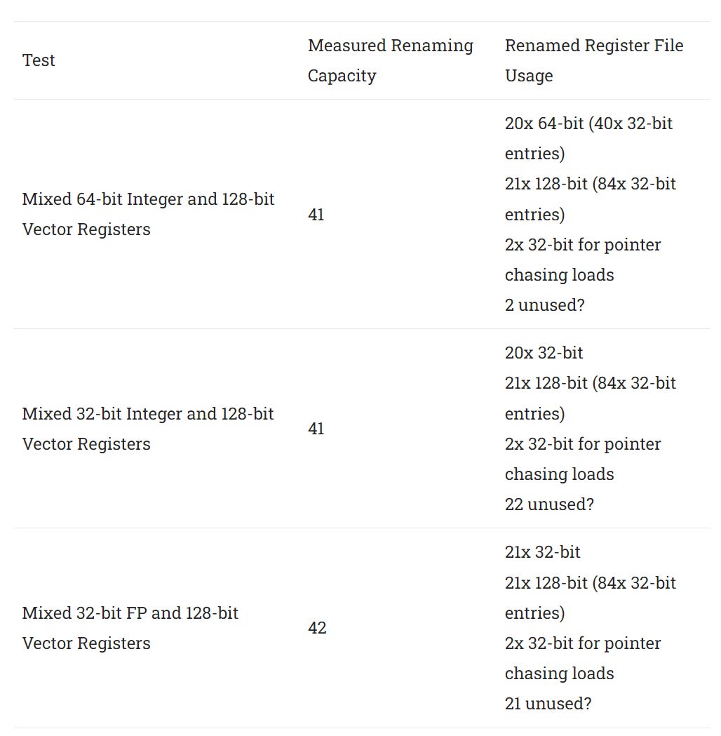
Depending on how smaller registers are allocated, the renamer might not be able to find a contiguous aligned block of four 32-bit registers when it needs space to store a 128-bit value. So while A57 uses register storage more efficiently than modern CPUs, it’s not perfect.
When instructions retire, their results are copied from the renamed register file into a separate architectural register file (ARF). Like on Intel’s original P6, this scheme is potentially easier to implement because renamed registers can be freed when an instruction retires. Exception recovery is also easy because known-good register state is held in one place. However, the ARF scheme requires more data movement and thus consumes more power. Intel moved to a PRF scheme with Sandy Bridge, and Arm did the same with Cortex A73.
Arm’s newer Cortex A72 possibly uses a scheme similar to the A57. I went back over data collected on that CPU and there are certainly similarities to A57 data. When I tested the A72, I rushed because I was paying for a Graviton 1 cloud instance, and thus had limited time to write different tests to explore the core. I’ll have to revisit A72 when work and real life demands give me a break.
Schedulers
A57 uses a mostly distributed scheduling scheme with small dedicated schedulers feeding each execution unit. Most of the schedulers have eight entries. The two exceptions are the branch scheduler, which has 12 entries, and the load/store AGUs, which share a 16 entry scheduling queue. Scheduling capacity is likely to limit A57’s reordering capacity before the register file or reorder buffer fills.

Integer Execution Units
Like many low power CPUs, A57 has two integer pipelines capable of handling the most common operations. Multi-cycle integer operations go to a separate pipe. Multiplies go down this pipe and take five cycles to produce a 64-bit result. Branches get a separate port as well, likely to ensure they’re resolved as quickly as possible to minimize mispredict penalties.

In theory, A57 can execute four integer operations per cycle. In practice, that will rarely occur because branches and multi-cycle integer operations are far less common than simple ones.
Floating Point and Vector Execution
FP and vector operations are handled by a pair of ports, each fed by an 8 entry scheduler. Arm’s optimization manual suggests both ports can handle basic FP operations like addition and multiplication, but I was unable to get two scalar FP operations per cycle. 128-bit packed FP operations also execute at one per cycle, so Cortex A57 does have 128 bits of total FP throughput but strangely can’t execute two FP instructions per cycle.

ARM’s ASIMD/NEON instruction set provides fmla and fmadd instructions for fused multiply add operations. These execute at one per cycle on Cortex A57, doubling FP throughput. However, latency is very high at 10 cycles.
Vector integer operations enjoy better performance. Both pipelines can handle 128-bit packed integer adds and other basic operations. Latency however is still high. Vector integer adds have 3 cycles of latency, and multiplies have four cycle latency. 128-bit packed integer multiplies only use the first FP pipe, and execute at a rate of one per two cycles.
Load/Store
Memory operations are handled by a pair of pipelines. One handles loads and the other handles stores. Cortex A57 can have 32 loads and 12 stores in-flight. The small store queue size will likely limit reordering capacity. Zen 4 already sees its store queue fill often. If we consider that A57 is designed to keep around 128 instructions in flight, the store queue covers less of the core’s reordering window than on Zen 4.
Unlike newer Arm cores and contemporary desktop CPUs, Cortex A57 doesn’t try to predict whether memory operations will be independent. Therefore, loads are stalled until all prior store addresses have been resolved. For dependent loads, store forwarding latency is typically seven cycles. Forwarding latency is doubled if a load partially overlaps a 16B aligned store, but otherwise there are no notable slow paths.

Cortex A57 translates program-visible 48-bit virtual addresses to 44-bit physical addresses with a fully associative 32 entry DTLB. With 4K pages, those 32 entries should cover 128 KB of address space. DTLB misses can be caught by a unified 1024 entry 4-way set associative L2 TLB. This L2 TLB also handles misses from the instruction TLB.
44-bit physical addressing lets Cortex A57 address up to 16 TB of memory. Arm’s newer cores like the Cortex X2 only support 40-bit physical addresses, with larger physical address capability reserved for Arm’s Neoverse line. A57 was expected to take on both client and server roles, and had to make a compromise.
Cache and Memory Latency
Memory accesses first check Cortex A57’s 32 KB 2-way set associative data cache. The data cache has optional ECC protection with 4 byte granularity. Data cache accesses generally have four cycle latency, or 5 cycles for indexed addressing. A57 suffers heavily from address translation penalties when using 4K pages. Latency spikes to 16 cycles at the 12 KB test size. The spike goes away when using huge pages, suggesting we’re somehow getting TLB misses even though the test array should be well within TLB coverage.

L1 misses go to a shared 2 MB L2 cache. The L2 has mandatory ECC protection for both data and tags, helping with data integrity. To save on area and power, the L2 cache uses a random replacement policy. That means the cache doesn’t have to store metadata on which lines were most recently or frequently used, but can lead to sub-optimal decisions on what data to kick out when bringing new lines in.
Arm lets implementers configure L2 latency to keep clocks up with larger L2 options. It’s impossible to tell if Nvidia used any of these register slicing options, but testing showed the L2 has 22 cycles of load-to-use latency. However, adding L2 TLB latency brings this to over 50 cycles. Finally, DRAM access takes around 250 cycles.
Intel’s Skylake is roughly contemporary with Nvidia’s Tegra X1 and enjoys better latency throughout the memory hierarchy. Access to the i5-6600K’s 6 MB last level cache takes about 11.2 ns, and that includes a few cycles to get an address translation from the L2 TLB.

Memory latency on the Nintendo Switch is high by desktop standards. LPDDR4 likely contributes to higher latency, but is a necessary design choice for a bandwidth hungry low power device.
Core to Core Latency
Multi-core systems have to ensure all cores have a coherent view of memory. Cortex A57’s L2 cache handles this by being strictly inclusive of L1 data cache contents, and maintaining duplicate copies of the L1 data cache tag arrays. We can test how fast two cores can exchange data by using __sync_bool_compare_and_swap to bounce a value between them.

Even though transfers are taking place within a core cluster, latency is higher than cross-cluster latency on AMD’s Zen.

That said, a good program will avoid shuffling data between cores. Tegra X1’s higher core to core latency should have minimal impact on performance.
Bandwidth
Cortex A57’s L1 data cache can service a load and a store every cycle. With 128-bit vector accesses, that gives 28 GB/s of L1D read bandwidth. Strangely, L1 bandwidth falls off after 16 KB. As with latency, using hugepages makes the dip go away, suggesting address translation penalties are cutting into bandwidth. I saw the same behavior with A72.

Cortex A57’s cluster-wide L2 cache is 16-way set associative, and has 2 MB of capacity on the Tegra X1. The L2 tags are divided into two banks, letting it service two requests per cycle. Each tag bank covers four data banks. For a single core, the L2 can provide about 8 bytes per cycle of read bandwidth.

Thanks to banking, we get a nice bandwidth increase with two cores loaded. However, L2 bandwidth increases taper off as we load more cores. In contrast, Intel’s L3 cache has as many banks as there are cores, allowing for excellent bandwidth scaling. The Core i5-6600K’s L3 can deliver a massive amount of bandwidth, and a single Skylake core can get more cache bandwidth than all four of Tegra X1’s Cortex A57 cores combined.

Intel’s quad-banked L3 cache delivers better per-cycle performance too, at just above 62 bytes per cycle with a memory bandwidth test running across four cores. Cortex A57’s shared L2 is stuck at 15.72 bytes per cycle. L2 write bandwidth is somewhat lower likely due to overhead from read-for-ownership requests.

L2 misses are generally satisfied by the DRAM controller. Tegra X1’s LPDDR4 setup should provide 25.6 GB/s of theoretical bandwidth. From the CPU cores, we get just under 30% of that figure. Bandwidth stops increasing after 2 to 3 cores are loaded, and tops out below 8 GB/s.

For comparison, a Core i5-6600K with dual channel DDR4-2133 achieved 28.6 GB/s in the same test. That’s 83% of the theoretical 34.1 GB/s available. Incredibly, Skylake enjoys higher memory bandwidth than Cortex A57 does from its L2.

Write bandwidth shows a similar story. A57’s memory bandwidth continues to be poor and far below what Skylake enjoys.

AMD’s Jaguar provides another comparison point. It similarly uses a 2 MB shared L2 cache, but AMD enjoys twice as much L2 bandwidth. Tegra X1 implements a more modern 64-bit LPDDR4 interface compared to Jaguar’s single channel DDR3 setup, but Cortex A57 fails to achieve higher memory bandwidth.
Some Light Benchmarking
I’m gonna pivot here with a focus on core width. We already know how Skylake will stack up against Cortex A57 if I benchmark the two head to head. A comparison to Arm’s later Cortex A73 should be more fun, because A73 is a 2-wide core that shares some weaknesses with A57 like a small scheduler. That means A73 can’t match A57 in sustained throughput. However, A73 does run at a higher 2.2 GHz clock speed.
Here, I’m testing how long it takes for 7-Zip to compress a large 2.67 GB file. To add some variety, I’m also using libx264 to transcode a 4K video down to 720P.

In the compression workload, Cortex A57 pulls ahead. Higher core width wins over a narrower but faster clocked core. However, it’s a small lead of less than 5%. With video encoding, A73 wins. But again, the difference is less than 5%. Cortex A73 has just 1 MB of L2 cache compared to A57’s 2 MB, so Arm’s newer core is doing quite well.
The close results are because A73 improves on aspects other than core width, and we can dig into that using performance counters. As an aside, performance counters aren’t comparable across reviews because I’m selecting the closest set of events to best compare the two cores. For example, Cortex A57 cannot count branches and branch mispredicts at retirement. It only has events that count at the execute stage. A73 introduces at-retirement events for branches and mispredicted branches.
At the start of the pipeline, A73 has a stronger branch predictor. Mispredicts per instruction decreased by 20% and 27% in 7-Zip and libx264 respectively. A73 thus wastes less power and time working on the wrong stuff.

At the instruction fetch stage, A73 loses width but increases instruction cache capacity to 64 KB. For libx264, this reduces instruction cache misses per instruction by 53%. Fetching from L2 or beyond costs more power than doing so from a first level cache, so A73 cuts down power spent moving instruction bytes around.

7-Zip also benefits from a larger instruction cache, but A57’s 48 KB cache was already large enough.
The data side sees less change. A73 and A57 both have a 32 KB data cache, so hitrates are similar. Both tested applications see quite a few L1D refills, but libx264 struggles more.

Finally, we can look at L2 misses. I’m using the l2d_cache_refill event from perf on both CPUs, but what the event is counting doesn’t seem comparable across the two CPUs. Cortex A73 counts more L2 data refills than L1D refills, so it could have a very aggressive L2 prefetcher.

Cortex A57’s L2 prefetcher can generate up to eight prefetches after a L2 miss, though all have to be within the same 4K page. Arm’s Cortex-A73 MPCore Processor Technical Reference Manual mentions a L2 prefetcher, but doesn’t say if it’s more aggressive. However, A73’s L2 can support 48 pending fills, while A57’s can only support up to 20. A73 could be exploiting that increased memory level parallelism capability to reduce performance loss from a smaller L2.
Final Words
Taken in isolation, Arm’s Cortex A57 is a decent low power core with excellent register renaming capacity for 32-bit integer code and passable branch prediction. Within the execution engine, the core’s main weaknesses are high execution latency for floating point instructions, small scheduler capacity, and a small store queue. Some of those weaknesses are present on other low power designs too, so it’s hard to fault Arm for that.
Where Cortex A57 really struggles is the memory subsystem. At a high level, the core-private 32 KB data caches and 2 MB shared last level cache are typical for a low power design. AMD uses a similar setup in Jaguar a few years prior. However, A57’s TLB setup suffers from extremely poor performance. The core suffers inexplicable L1 DTLB misses even when accessing arrays that should fit within its 128 KB coverage. When L1 DTLB msises happen, the 1024 entry L2 TLB performs poorly and adds over 20 extra cycles of latency. L2 TLBs on most other CPUs have less than 10 cycles of latency. Finally, both the L2 cache and system memory suffer from poor bandwidth.
As a low power cell phone and tablet core, Cortex A57 is an acceptable design for its time. Subsequent years would see Arm develop increasingly performant low power cores as improvements in process technology allowed more sophisticated microarchitectures to fit within a few watts.
As the Nintendo Switch’s CPU, Cortex A57 is weak and not comparable to even outdated desktop cores. Modern game developers are able to port games to this platform, but that no doubt involves tons of optimization work. Hogwarts Legacy for example released on Switch around nine months after its initial release on PC. Even then, the required optimizations make the Switch version almost a different game.

Still, it’s a wonder that developers managed to get games like Hogwarts Legacy working on the switch at all. I wonder if similar optimization efforts could be carried out to make modern games accessible to a wider audience. A lot of gamers don’t have infinite budgets, and could be using integrated graphics on old CPUs. Switch-like optimizations could make AAA games playable on those platforms.
If you like our articles and journalism, and you want to support us in our endeavors, then consider heading over to our Patreon or our PayPal if you want to toss a few bucks our way. If you would like to talk with the Chips and Cheese staff and the people behind the scenes, then consider joining our Discord.