
AMD’s CDNA 3 Compute Architecture


AMD has a long history of vying for GPU compute market share. Ever since Nvidia got first dibs with their Tesla architecture, AMD has been playing catch up. Terascale 3 moved from VLIW5 to VLIW4 to improve execution unit utilization in compute workloads. GCN replaced Terascale and emphasized consistent performance for both GPGPU and graphics applications. Then, AMD diverged their GPU architecture development into separate CDNA and RDNA lines specialized for compute and graphics respectively.

CDNA 2 finally brought AMD notable success. MI250X and MI210 GPUs won several supercomputer contracts including ORNL’s Frontier, which holds first place on November 2023’s TOP500 list. But while CDNA2 delivered solid and cost efficient FP64 compute, H100 had better AI performance and offered a larger unified GPU.
CDNA 3 looks to close those gaps by bringing forward everything AMD has to offer. The company’s experience in advanced packaging technology is on full show, with MI300X getting a sophisticated chiplet setup. Together with Infinity Fabric components, advanced packaging lets MI300X scale to compete with Nvidia’s largest GPUs. On the memory side, Infinity Cache from the RDNA line gets pulled into the CDNA world to mitigate bandwidth issues. But that doesn’t mean MI300X is light on memory bandwidth. It still gets a massive HBM setup, giving it the best of both worlds. Finally, CDNA 3’s compute architecture gets significant generational improvements to boost throughput and utilization.
GPU Layout
AMD has a tradition of using chiplets to cheaply scale core counts in their Ryzen and Epyc CPUs. MI300X uses a similar strategy at a high level, with compute split off onto Accelerator Complex Dies, or XCDs. XCDs are analogous to CDNA 2 or RDNA 3’s Graphics Compute Dies (GCDs) or Ryzen’s Core Complex Dies (CCDs). AMD likely changed the naming because CDNA products lack the dedicated graphics hardware present in the RDNA line.

Each XCD contains a set of cores and a shared cache. Specifically, every XCD physically has 40 CDNA 3 Compute Units, with 38 of these being enabled per XCD on the MI300X. A 4 MB L2 cache sits on the XCD as well, and serves all of the die’s CUs. MI300X has eight XCDs, giving it 304 total Compute Units.

That’s a large increase over the MI250X’s 220 CUs. Even better, MI300X can expose all of those CUs as a single GPU. On MI250X, a programmer would have to manually split up work across the two GPUs because each has a separate pool of memory.

Nvidia’s H100 consists of 132 Streaming Multiprocessors (SMs) and also presents them to programmers as a big unified GPU. H100 takes a conventional approach by implementing all of that compute on a large monolithic die. Even with everything on the same die, H100 is too large to give all of its SMs equal access to cache. So, H100 splits the L2 into two instances. A single SM can use all 50 MB of L2, but access to more than 25 MB will incur a performance penalty.

Still, Nvidia’s strategy makes more efficient use of cache capacity than MI300X’s. A MI300X XCD doesn’t use L2 capacity on other XCDs for caching, just as CCDs on Epyc/Ryzen don’t allocate into each other’s L3 caches.
Intel’s Ponte Vecchio (PVC) compute GPUs make for a very interesting comparison. PVC places its basic compute building blocks in dies called Compute Tiles, which are roughly analogous to CDNA 3’s XCDs. Similarly, PVC’s Base Tile serves a similar function to CDNA 3’s IO dies. Both contain a large last level cache and HBM memory controllers. Like MI300X, a Ponte Vecchio card can be exposed as a single GPU with a unified memory pool.

However, there are important differences. Ponte Vecchio’s Compute Tiles are smaller with only eight Xe Cores, compared to 38 Compute Units on a CDNA 3 XCD. Instead of using a Compute Tile wide cache, Intel uses larger L1 caches to reduce cross-die traffic demands. Using a two-stack Ponte Vecchio part as a unified GPU presents challenges too. The EMIB bridge between the two stacks only offers 230 GB/s of bandwidth, which isn’t enough to fully utilize HBM bandwidth if accesses are striped across all memory controllers. To address this, Intel has APIs that can let programs work with the GPU in a NUMA configuration.
In terms of physical construction, PVC and CDNA 3’s designs have different challenges. CDNA 3’s ability to present a unified memory pool with HBM requires high bandwidth between the IO dies. PVC gets by with a relatively low bandwidth EMIB link. But PVC’s design gets complicated because it uses four die types with different process nodes and foundries. AMD only uses two die types in MI300X, and both nodes (6 nm and 5 nm) are from TSMC.
Tackling the Bandwidth Problem
Compute has been outpacing memory for decades. Like CPUs, GPUs have countered this with increasingly sophisticated caching strategies. CDNA 2 used a conventional two-level cache hierarchy with a 8 MB L2, relying on HBM2e to keep the execution units fed. But even with HBM2e, MI250X was more bandwidth starved than Nvidia’s H100. If AMD simply added more compute, bandwidth starvation could be come a serious issue. So, AMD took a leaf out of RDNA(2)’s book and added an “Infinity Cache”.
Much like the consumer RDNA GPUs, MI300’s Infinity Cache is what the technical documentation calls Memory Attached Last Level (MALL), which is a fancy way to say that the last level cache level is a memory side cache. Compared to L1 and L2 caches that are closer to the Compute Units, the Infinity Cache is attached to the memory controllers. All memory traffic passes through the Infinity Cache regardless of what block it’s coming from. That includes IO traffic, so communications between peer GPUs can benefit from Infinity Cache bandwidth. Because the Infinity Cache always has the most up to date view of DRAM contents, It doesn’t have to handle snoops or other cache maintenance operations.

But because a memory side cache is farther away from compute, it generally suffers from higher latency. Therefore, AMD has multi-megabyte L2 caches on both CDNA 3 and RDNA 2 to insulate compute from the lower performance of a memory side cache.
Like RDNA 2, CDNA 3’s Infinity Cache is 16-way set associative. However, CDNA 3’s implementation is more optimized for bandwidth than capacity. It’s composed of 128 slices, each with 2 MB of capacity and 64 bytes per cycle of read bandwidth. All of the slices together can deliver 8192 bytes per cycle, which is good for 17.2 TB/s at 2.1 GHz.

For comparison, RDNA 2’s 128 MB Infinity Cache can provide 1024 bytes per cycle across all slices, giving it 2.5 TB/s of theoretical bandwidth at 2.5 GHz. Die shots suggest each Infinity Cache slice has 4 MB of capacity and provides 32B/cycle. RDNA 2 therefore uses bigger slices, fewer of them and has less bandwidth from each slice.
MI300X’s focus on bandwidth means workloads with lower compute density can still enjoy decent performance if they can get enough Infinity Cache hits. That should make CDNA 3’s execution units easier to feed even though the main memory bandwidth to compute ratio hasn’t changed much and remains behind Nvidia’s.

If we construct a roofline model for MI300X using Infinity Cache’s theoretical bandwidth, we can achieve full FP64 throughput with 4.75 FLOPs per byte loaded. It’s a massive improvement over DRAM, which would require 14.6 to 15 FLOPs per byte loaded.
Possible Challenges with Cross-Die Bandwidth
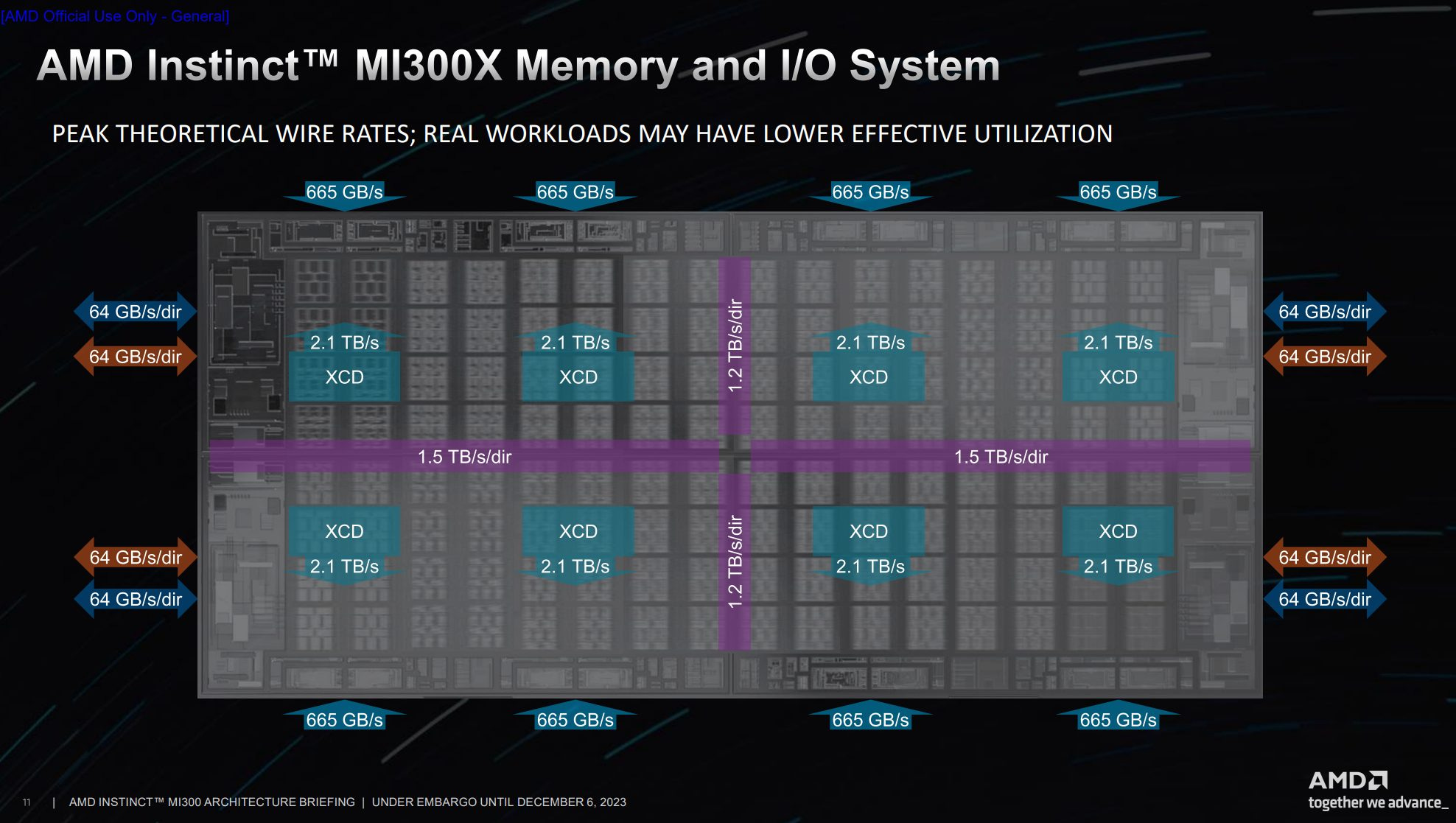
MI300X’s Infinity Fabric spans four IO dies, each of which connects to two HBM stacks and associated cache partitions. However, the bandwidth of the die to die connections may limit achieving full Infinity Cache bandwidth when MI300X operates as a single logical GPU with a unified memory pool. If memory accesses are striped evenly across the memory controllers (and thus cache partitions), as is typical for most GPU designs, the available die-to-die bandwidth may prevent applications from reaching theoretical Infinity Cache bandwidth.

First, let’s focus on a single IO die partition. It has 2.7 TB/s of ingress bandwidth along two edges adjacent to other IO dies. Its two XCDs can get 4.2 TB/s of Infinity cache bandwidth. If L2 miss requests are evenly striped across the dies, 3/4 of that bandwidth, or 3.15 TB/s, must come from peer dies. Since 3.15 TB/s is greater than 2.7 TB/s, cross-die bandwidth will limit achievable cache bandwidth.

We can add the die in the opposite corner without any differences because all of its required die-to-die bandwidth goes in the opposite direction. MI300X has bidirectional die-to-die links.

If all dies demand maximum Infinity Cache bandwidth in a unified configuration, things get more complex. Extra cross-die bandwidth is consumed because transfers between dies in opposite corners require two hops, and that’ll cut into ingress bandwidth available for each die.
While MI300X was engineered to act like one big GPU, splitting MI300X into multiple NUMA domains could give higher combined Infinity Cache bandwidth. It’s possible that AMD will have an API that will transparently split up programs among the different IO dies. Additionally, the likelihood of bandwidth issues would be minimized by high L2 hit rates, which would help avoid those bottlenecks. And in cases where the Infinity Cache hit rate are low, the MI300X’s die-to-die links are sufficiently robust and offer ample bandwidth to smoothly handle HBM traffic.
Cross-XCD Coherency
Even though the Infinity Cache doesn’t have to worry about coherency, the L2 caches do. Ordinary GPU memory accesses follow a relaxed coherency model, but programmers can use atomics to enforce ordering between threads. Memory accesses on AMD GPUs can also be marked with a GLC bit (Global Level Coherent). Those mechanisms still have to work if AMD wants to expose MI300X as a single big GPU, rather than a multi-GPU configuration as MI250X had done.

On prior AMD GPUs, atomics and coherent accesses were handled at L2. Loads with the GLC bit set would bypass L1 caches, and thus get the most up-to-date copy of data from L2. That doesn’t work with MI300X because the most up-to-date copy of a cacheline could be on another XCD’s L2 cache. AMD could make coherent accesses bypass L2, but that would lower performance. That may have worked for a gaming GPU where coherent accesses aren’t too important. But AMD wants MI300X to perform well with compute workloads, and needs MI300A (the APU variant) to efficiently share data between the CPU and GPU. That’s where Infinity Fabric comes in.

Like Infinity Fabric on Ryzen, CDNA 3 has Coherent Masters (CMs) where the XCDs connect to the IO dies. Coherent Slaves (CS) sit at each memory controller alongside Infinity Cache (IC) slices. We can infer how these work via Ryzen documentation, which shows Coherent Slaves have a probe filter and hardware for handling atomic transactions. MI300X likely has a similar CS implementation.

If a coherent write shows up at the CS, it has to ensure any thread doing a coherent read will observe that write regardless of where that thread is running on the GPU. That means any XCD with the line cached will have to reload it from Infinity Cache to get the most up to date data. Naively, the CS would have to probe L2 caches across all XCDs because any of them could have the corresponding data cached. The probe filter helps avoid this by tracking which XCDs actually have the line cached, thus avoiding unnecessary probe traffic. CDNA 3’s whitepaper says the snoop filter (another name for a probe filter) is large enough to cover multiple XCD L2 caches. I certainly believe them because MI300X has 32 MB of L2 across all eight XCDs. Even consumer Ryzen parts can have more CCD-private cache for the probe filter to cover.
Thanks to CPU-like Infinity Fabric components like CS and CM, a XCD can have a private write-back L2 cache capable of handling intra-die coherent accesses without going across the IO die fabric. AMD could have gone for a naive solution where coherent operations and atomics go straight to the Infinity Cache, bypassing L2. Such a solution would save engineering effort and create a simpler design at the cost of lower performance for coherent operations. Evidently, AMD thought optimizing atomics and coherent accesses was important enough to go the extra mile.
To ensure coherence of local memory writes of CUs in different agents a
buffer_wbl2 sc1is required. It will writeback dirty L2 cache lines.To ensure coherence of local memory reads of CUs in different agents a
buffer_inv sc0 sc1is required. It will invalidate non-local L2 cache
lines if configured to have multiple L2 caches.LLVM Documentation for the GFX942 Target
However, CDNA 3 within the XCD still works a lot like prior GPUs. Evidently normal memory writes will not automatically invalidate written lines from peer caches as in CPUs. Instead, code must explicitly tell the L2 to write back dirty lines and have peer L2 caches invalidate non-local L2 lines.
L2 Cache
Closer to the Compute Units, each MI300X XCD packs a 4 MB L2 cache. The L2 is a more traditional GPU cache, and is built from 16 slices. Each 256 KB slice can provide 128 bytes per cycle of bandwidth. At 2.1 GHz, that’s good for 4.3 TB/s. As the last level of cache on the same die as the Compute Units, the L2 plays an important role in acting as a backstop for L1 misses.

Compared to H100 and MI250X, MI300X has a higher L2 bandwidth to compute ratio. Because each XCD comes with a L2, L2 bandwidth naturally scales as a CDNA 3 product comes with more XCDs. In other words, MI300X’s L2 arrangement avoids the problem of getting a single cache hooked up to a lot of Compute Units and maintain a ton of bandwidth.
PVC’s L2 is a clear contrast. As Intel adds more Compute Tiles, the Base Tile’s shared L2 gets increasing bandwidth demands. From a cache design standpoint, PVC’s configuration is simpler because the L2 acts as a single point of coherency and a backstop for L1 misses. But it can’t offer as much bandwidth as MI300X’s L2. MI300X also likely enjoys better L2 latency, making it easier for applications to utilize cache bandwidth.
L1 Cache
CDNA 3’s focus on high cache bandwidth continues to the L1. In a move that matches RDNA, CDNA 3 sees its L1 throughput increased from 64 to 128 bytes per cycle. CDNA 2 increased per-CU vector throughput to 4096 bits per cycle compared to 2048 in GCN, so CDNA 3’s doubled L1 throughput helps maintain the same compute to L1 bandwidth ratio as GCN.

Besides higher bandwidth, CDNA 3 increases L1 capacity from 16 to 32 KB. It’s a move that again mirrors developments in the RDNA line, where RDNA 3 received a similar size boost for its first level cache. Higher hitrates from the larger cache would lower average memory access latency, improving execution unit utilization. Transferring data from L2 and beyond costs power, so higher hitrate can help power efficiency too.
While CDNA 3 improves first level caching, Ponte Vecchio is still the champion in that category. Each Xe Core in PVC can deliver 512 bytes per cycle, giving Intel a very high L1 bandwidth to compute ratio. The L1 is large as well at 512 KB. Memory bound kernels that fit in L1 will do very well on Intel’s architecture. However, Ponte Vecchio lacks a mid-level cache at the Compute Tile level, and could face a harsh performance cliff as data spills out of L1.
Scheduling and Execution Units
A complex chiplet setup and modified cache hierarchy let AMD present MI300X as a single GPU, thus addressing one of MI250X’s biggest weaknesses. But AMD didn’t settle with that. They also made iterative improvements to the core Compute Unit architecture, addressing CDNA 2’s difficulties with utilizing its FP32 units.

When CDNA 2 shifted to handling FP64 natively, AMD provided double rate FP32 via packed execution. The compiler would have to pack two FP32 values into adjacent registers and perform the same instruction on both. Often, the compiler struggled to pull this off unless programmers explicitly used vectors.
CDNA 3 gets around this with a more flexible dual issue mechanism. Most likely, this is an extension of GCN’s multi-issue capability rather than RDNA 3’s VOPD/wave64 method. Each cycle, the CU scheduler selects one of the four SIMDs and checks whether any of its threads are ready to execute. If multiple threads are ready, GCN could select up to five of them to send to execution units. Of course a GCN SIMD only has a single 16-wide vector ALU, so GCN would have to select threads with different instruction types ready to multi-issue. For example, a scalar ALU instruction can issue alongside a vector ALU one.
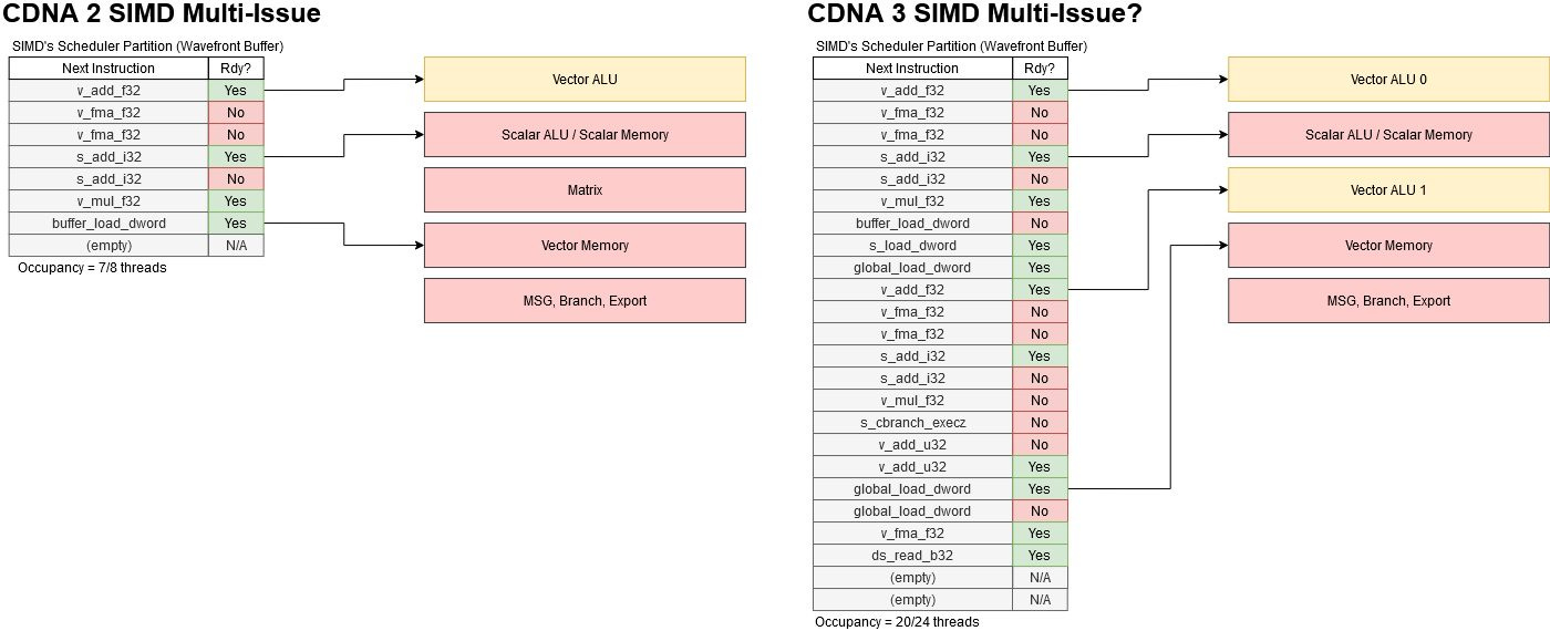
An alternative approach would be to take advantage of wave64’s wider width and let a thread complete two vector instructions over four cycles. However, doing so would break GCN’s model of handling VALU instructions in multiples of 4 clock cycles. CDNA 3 is still more closely related to GCN than RDNA is, and reusing GCN’s multi-issue strategy is a sensible move. AMD also could have used RDNA 3’s VOPD mechanism, where a special instruction format can contain two operations. While that method could increase per-thread performance, relying on the compiler to find dual issue pairs could be hit or miss.

Instead of relying on the compiler, CDNA 3’s dual issue approach likely pushes responsibility to the programmer to expose more thread level parallelism via larger dispatch sizes. If a SIMD has more threads in flight, it’ll have a better chance of finding two threads with FP32 instructions ready to execute. At minimum, a SIMD will need two threads active to achieve full FP32 throughput. In practice CDNA 3 will need much higher occupancy to achieve good FP32 utilization. GPUs use in-order execution so individual threads will often be blocked by memory or execution latency. Keeping one set of execution units fed can be difficult even at full occupancy.

Therefore, AMD has dramatically increased the number of threads each CDNA 3 SIMD can track from 8 to 24. If a programmer can take advantage of this, CDNA 3 will be better positioned to multi-issue. But this can be difficult. AMD did not mention an increase in vector register file capacity, which often limits how many threads a SIMD can have in flight. The vector register file can hold state for more threads if each thread uses fewer registers, so CDNA 3’s multi-issue capability may work best for simple kernels with few live variables.
Register file bandwidth presents another challenge for dual issue. CDNA 2’s packed FP32 execution didn’t require extra reads from the vector register file because it took advantage of wider register file ports needed to deliver 64-bit values. But separate instructions can reference different registers and require more reads from the register file. Adding more register file ports would be expensive, so CDNA 3 “generationally improves the source caching to provide better re-use and bandwidth amplification so that each vector register read can support more downstream vector or matrix operations”1. Most likely, AMD is using a larger register cache to mitigate port conflicts and keep the execution units fed.
Matrix Operations
Matrix multiplication has become increasingly important as machine learning picks up. Nvidia invested heavily in this area, adding matrix multiplication units (tensor cores) to their Volta and Turing architectures years ago. AMD’s CDNA architecture added matrix multiply support, but contemporary Nvidia architectures invested more heavily in matrix multiplication throughput. This especially applies to lower precision data types like FP16, which are often used in AI.

MI300X plays catch up by doubling per-CU matrix throughput compared to prior CDNA generations. On top of that, MI300X’s chiplet design allows a massive number of CUs. But Nvidia’s higher per-SM matrix performance still makes it a force to be reckoned with. Therefore, CDNA 3 continues AMD’s trend of hitting Nvidia hard from the vector FP64 performance side while maintaining strong AI performance in isolation.
Instruction Cache
Besides handling memory accesses requested by instructions, a Compute Unit has to fetch the instructions themselves from memory. GPUs traditionally had an easier time with instruction delivery because GPU code tends to be simple and not occupy a lot of memory. In the DirectX 9 era, Shader Model 3.0 even imposed limits on code size. As GPUs evolved to take on compute, AMD rolled out their GCN architecture with 32 KB instruction caches. Today, CDNA 2 and RDNA GPUs continue to use 32 KB instruction caches.
CDNA 3 increases instruction cache capacity to 64 KB. Associativity doubles too, from 4-way to 8-way. That means higher instruction cache hitrates for CDNA 3 with bigger, more complex kernels. I suspect AMD is targeting CPU code naively ported to GPUs. Complex CPU code can be punishing on GPUs, since they can’t hide instruction cache miss latency with long distance instruction prefetching and accurate branch prediction. Higher instruction cache capacity helps contain larger kernels, while increased associativity helps avoid conflict misses.
Like CDNA 2, each CDNA 3 instruction cache instance services two Compute Units. GPU kernels are usually launched with large enough work sizes to fill many Compute Units, so sharing the instruction cache is a good way to efficiently use SRAM storage. I suspect AMD didn’t share the cache across even more Compute Units because a single cache instance may struggle to satisfy instruction bandwidth demands.
Final Words
CDNA 3’s whitepaper says that “the greatest generational changes in the AMD CDNA 3 architecture lie in the memory hierarchy” and I would have to agree. While AMD improved the Compute Unit’s low precision math capabilities compared to CDNA 2, the real improvement was the addition of the Infinity Cache.
MI250X’s primary issue was that it wasn’t really one GPU. It was two GPUs sharing the same package which only has 200 Gigabyte per second per direction between the GCDs. In AMD’s assessment that 200 Gigabyte per second per direction was not enough to have the MI250X show up as one GPU which is why AMD significantly increased the die to die bandwidth.
AMD increased the total East-West bandwidth to 2.4TB/sec per direction which is a 12 fold increase from MI250X. And the total North-South bandwidth is an even higher 3.0TB/sec per direction. With these massive bandwidth increases, AMD was able to make the MI300 appear as one large, unified accelerator instead of as 2 separate accelerators like MI250X.
4.0 TB/s of total ingress bandwidth for one die may not seem like enough if both XCD needs all available memory bandwidth. However, both XCDs combined can only access up to 4.2TB/s of bandwidth from the IO die so realistically the 4.0TB/s of ingress bandwidth is a non-issue. What the maximum of 4.0TB/s of ingress bandwidth does mean is that a single IO die can’t take advantage of all 5.3TB/s of memory bandwidth.
This is similar to desktop Ryzen 7000 parts where one CCD can’t take full advantage of DDR5 bandwidth due to Infinity Fabric limits. However this is likely to be a non-issue on MI300X because the bandwidth demands will be highest with all dies in play. In that case, each die will consume about 1.3 TB/s of bandwidth and getting 3/4 of that over cross-die links won’t be a problem.
But MI300 isn’t just a GPGPU part, it also has an APU part as well, which is in my opinion is the more interesting of the two MI300 products. AMD’s first ever APU, Llano, was released in 2011 which was based on AMD’s K10.5 CPU paired with a Terascale 3 GPU. Fast forward to 2023 and for their first “big iron” APU, the MI300A, AMD paired 6 of their CDNA3 XCDs with 24 Zen 4 cores all while reusing the same base die. This allows for the CPU and the GPU to shared the same memory address space which removes the need to copy data over an external bus to keep the CPU and GPU coherent with each other.
We look forward to what AMD could do with future “big iron” APUs as well as their future GPGPU line up. Maybe they’ll have specialized CCDs with wider vector units or maybe they’ll have networking on their base die that can directly connect to the xGMI switches that Broadcom have said to be making. Regardless of what future Instinct products look like, we are excited to both be looking forward to those products as well as testing the MI300 series.
We would like to thank AMD for inviting Chips and Cheese to the MI300 launch event. We were able to ask a lot of questions and gain some extra information without which this article would have been much shorter.
If you like our articles and journalism, and you want to support us in our endeavors, then consider heading over to our Patreon or our PayPal if you want to toss a few bucks our way. If you would like to talk with the Chips and Cheese staff and the people behind the scenes, then consider joining our Discord.
Hi, I can't find information about CDNA3's dual issue, where can i get it.