
AMD’s Athlon 64: Getting the Basics Right

Two decades ago, AMD’s K8 architecture went head to head against Intel’s best. But unlike the “Zen versus something-lake” situation today, the K8 versus Netburst situation is particularly interesting because the two cores took vastly different approaches to achieve high performance.
In this article, we’ll be looking at K8’s architecture using data from the AMD Athlon FX-62. This chip implemented two K8 cores on AMD’s own 90nm process, and ran at 2.8 GHz. It went head to head against Intel’s Netburst based chips in 2006, until Merom’s introduction later that year. We’ll also use some data from the AMD Athlon 64 6000+, which uses the same K8 cores on AMD’s 65 nm process.
Overview
The K8 architecture is largely the same as the K7 Athlon architecture, but with 64-bit support added, and a few tweaks here and there. The core is still built around executing x86 instructions that combine math and memory accesses, without decoding them into multiple micro-ops. The integer execution side is divided into three largely independent pipelines connected by a forwarding network.

Intel’s Netburst is also 3-wide, but is massive in every other way and packed to the brim with advanced microarchitecture features.

Frontend: Branch Prediction
K8 has a relatively short pipeline and is able to cancel instructions fetched from an incorrect path, so it suffers less from mispredicted branches than Intel’s Netburst. While branch prediction is still important to achieving high performance, AMD didn’t have to prioritize the branch predictor as much as Intel did.
From block diagrams and optimization manuals published by AMD, K7 and K8 both use a two level predictor with global history, where previous branch outcomes and the branch address are both used to index into a history table of 2-bit counters. However, K8 decreases the chance of aliasing by increasing history table size from 4096 to 16384 entries. AMD’s optimization manual says the history table is indexed using 4 bits of the branch address, and the outcome (taken or not taken) of the last eight branches. That only makes for 12 bits, which is funny because you’d need 14 bits to select one of the 16384 entries. Hans de Vries suggests that the “4 bits of the branch address” correspond to the 16 byte instruction cache line, which means the two unaccounted for bits would be used to select a branch within that line.
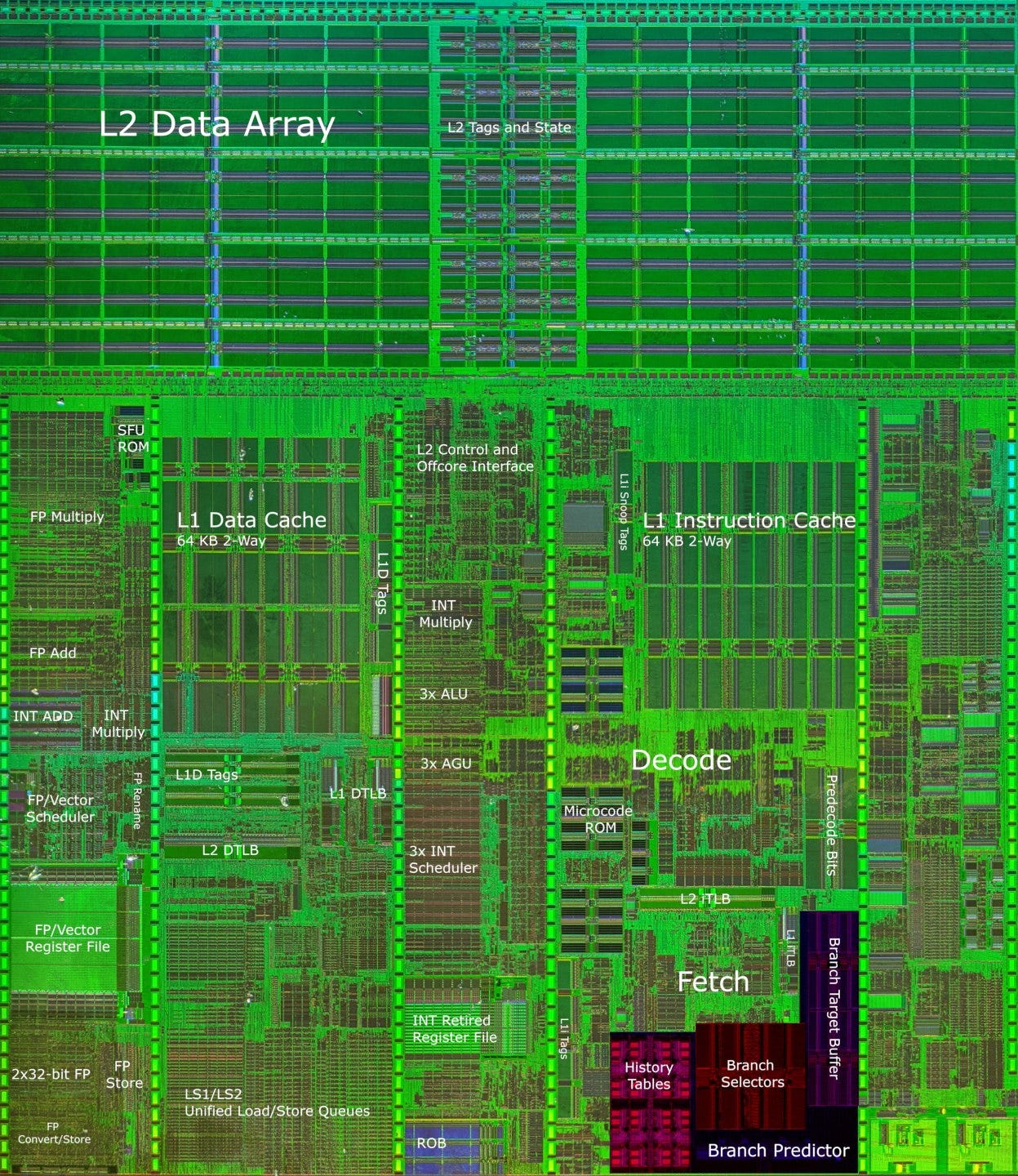
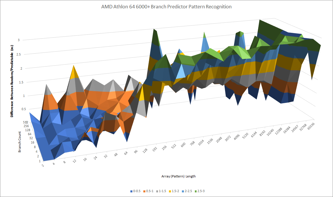
Overall, AMD’s Hot Chips slides claim a 5-10% branch prediction accuracy improvement over K7. We didn’t get particularly clean results, but K8’s pattern recognition capabilities clearly fall behind Netburst’s, which uses 16 bits of global history to index into its predictor.

To accelerate branch handling, K8 has a single-level BTB with 2048 entries. The BTB’s size is decent for a CPU of Athlon’s era, but it’s nothing to write home about. It can’t handle taken branches back to back. If a branch is taken, the frontend has to stall for a cycle while waiting for the target to come from the BTB. That makes loop unrolling important for AMD’s architecture. Modern architectures are usually able to handle at least a small number of taken branches without penalty, meaning that compiler optimizations like loop unrolling are less important.

Meanwhile, Netburst has incredible zero-bubble branch tracking capability, equal to that of Zen 3 in the best case. It also features a multi-level BTB that can track twice as many branch targets as K8 can, while clocking much higher. Netburst’s BTB design is a bit like modern designs, except for massive penalties when all doesn’t go according to plan.

AMD uses a BTB coupled to the L1 instruction cache, via branch selectors attached to instruction cache lines. On one hand, this scheme simplifies K8’s frontend because an instruction cache fetch also provides branch prediction information. However, it means no branch prediction information is available on an instruction cache miss. Since branches occur roughly every ten instructions, that makes it difficult to accurately prefetch ahead if there’s an instruction cache miss. Netburst likely uses a decoupled BTB design that lets the branch predictor act as a very accurate prefetcher as long as BTB capacity isn’t exceeded.
Overall, K8 has a decent branch predictor for a mid-2000s design. But Netburst’s predictor is in a different class. Intel has a more modern and sophisticated branch predictor setup, and equips it with much more storage to boot.
Frontend: Instruction Fetch
K8 uses an instruction cache that stores x86 instruction bytes, but moves some decoding stages in front of the instruction cache. As instructions are filled into the cache, a predecode stage does preliminary decoding. It determines instruction boundaries, opcode byte position, and instruction type, and stores that predecode data alongside instruction bytes. The main decoders have to do less, because the decoding job is partially done already.
This predecode scheme is a compromise that uses extra storage to simplify the main decoders, while keeping the caching capacity advantage of a conventional instruction cache. In contrast, Netburst’s trace cache makes an extreme tradeoff in the direction of maximizing fetch bandwidth, at the expense of caching capacity.

AMD’s instruction caching capacity advantage is actually much larger than the graph above would suggest, because a single memory location can be cached in several places within Intel’s trace cache. We also tested with 4 byte NOPs. In integer applications (7-Zip as an example), average executed instruction length is actually a tad under 4 bytes. Smaller instructions would increase AMD’s caching capacity, but doesn’t help Intel’s trace cache. Intel claims their trace cache has a hitrate similar to that of a 8 KB instruction cache.
Modern chips can use wide decoders and long distance prefetching to maintain high instruction bandwidth from L2. Unfortunately, K8’s coupled BTB prevents the core from accurately determining future fetch addresses after an L1i miss. That’s probably why AMD only supports two outstanding instruction cache misses (with two instruction MABs, or miss address buffers). K8 needs more memory level parallelism (MLP) from the instruction end to hide L2 latency, but more MLP would be wasted if the core can’t accurately prefetch. So, AMD ends up falling behind Netburst when instruction footprints fit within L2, but not L1i.
If faced with long instructions, K8 can also suffer L1i bandwidth limitations. To demonstrate this, here’s the test result with 8 byte NOPs, graphed in bytes per cycle. AMD can’t get close to 3 instructions per cycle (24 bytes per cycle) because the instruction cache can only provide 16 bytes per cycle. Netburst’s micro-op caching bypasses this limitation.

In fairness to AMD, this metric was less important in the early 2000s. K8 doesn’t need to handle long AVX or AVX-512 instructions, which are longer thanks to extra prefixes. “Long” instructions from Athlon’s era will often be ones with large immediates or displacements. And Netburst isn’t the best at handling those either. As detailed by Agner’s instruction manual, instructions with large immediates or displacements will sometimes take two entries in the trace cache.
Rename
Modern CPUs can pull a bag of tricks as micro-ops are allocated into the backend. Register to register copies can be eliminated, for example. But this is 2006, so we get the most important basics and nothing else. Common zeroing idioms are recognized and dependencies are broken, but that’s about it.
Execution Engine
In our article on Netburst, we talked about how it dropped P6’s ROB+RRF scheme in favor of a PRF one. K8 uses a hybrid of the two. The integer side behaves like P6, though K8’s RRF has enough ports to avoid register read bandwidth bottlenecks. The floating point and vector execution side uses a PRF, with the ROB holding pointers to entries in a separate vector register file. In practice, this distinction doesn’t matter. K8 has 120 FP registers, which is enough to cover the entire ROB after subtracting out entries needed to hold architectural state.

These 120 FP registers represent a large increase over K7’s 88 entry FP register file, but that was necessary because x86-64 brought more architectural registers. Specifically, there are now 16 architectural SSE registers, up from 8 on 32-bit x86. K8 therefore needed more entries to hold architectural state. Otherwise, the new core would end up being able to track fewer in-flight vector operations than its predecessor.
Aside from a bigger register file, K8 adds two entries to each integer scheduling queue, bringing total integer scheduling capacity to 24, up from 18 on K7. This is a welcome change, but the big picture is that K8 doesn’t change much compared to K7. It ends up very far behind Netburst’s reordering capacities – at least on paper.
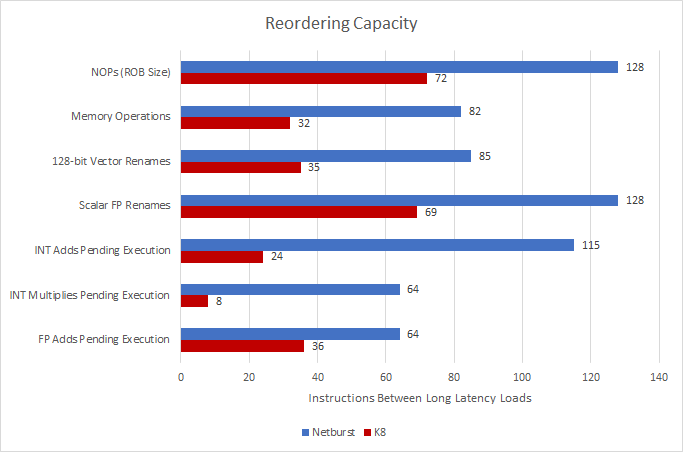
In theory, Intel will be far better at absorbing cache and memory latency. But Intel also can’t cancel bogus operations before retirement, so that reordering capacity will get wasted tracking instructions fetched from an incorrect path, even after a mispredict is discovered. If instructions on the bogus path have longer latency than that of a mispredict, Intel will lose reordering capacity from that. Finally, Intel may have opted for higher reordering capacity than was optimal for a single thread in order to increase SMT yield.
Integer Execution
On the integer side, AMD takes a brute force approach by creating three of almost everything. The ROB is organized as 24 lines, each with 3 micro-ops, and can be seen as a 3-lane design. The integer execution engine is basically three general purpose pipelines connected by a forwarding network, each capable of handling most x86 instructions. That includes instructions that combine math operations with memory accesses, so each pipeline features a small scheduling queue that feeds both an ALU and an AGU. Unlike Intel’s P6, load-op and load-op-store instructions are not broken into separate micro-ops. Instead, the instruction is kept as a single “macro-op”, and the scheduler dispatches it multiple times to its AGU and ALU pipes as necessary.

Because the execution engine doesn’t move instructions between pipelines, every ALUs has to handle the vast majority of integer operations. All of the ALUs have to accept both loads and stores. One notable exception is integer multiplies. Multipliers cost more die area, so only the first pipeline gets one, and the renamer puts all multiply operations into that pipeline.
AMD’s approach simplifies the design at several points. Most ALU instructions can go into any pipeline, so the renamer can allocate ops in round robin fashion without worrying about one pipeline getting too much work while the others sit idle. It could even keep an instruction in its “lane” from decode to retirement. I can also imagine a setup where the second and third renamer slots switch multiply ops to the first renamer slot when necessary, meaning that each renamer slot only has to track resources in its lane (and not the whole OOO engine). Also, scheduler and ALU/AGU blocks can be designed once and used three times.
There are real performance benefits too. Keeping load-op and load-op-store instructions as a single “macro-op” throughout the pipeline makes more efficient use of reordering resources. Those instructions would only occupy a single reorder buffer and scheduler entry, but would take two or more on early variants of Intel’s P6 architecture.
But this scheme means integer execution resources are excessively duplicated. The three AGUs that can never be fully utilized, because memory instruction throughput is limited by the dual-ported data cache. The ALUs are each beefier than they need to be to handle common instruction mixes. All three ALUs can handle not-taken jumps and shift instructions. Even uncommon integer instructions like CWD (convert word to doubleword via sign extension), BSWAP (used for converting between big and little endian), and SAHF (set flags) can execute at 3 per cycle on K8. For an idea of how ridiculous this allocation of execution resources is, Golden Cove only has 1 or 2 ports capable of handling those instructions.
Floating Point and Vector Execution
Like previous Athlon cores, K8’s FPU is implemented as a coprocessor that’s largely independent of the integer side. The FPU has its own renamer, scheduler, and registers. Floating point and vector instructions still require a ROB entry, but write their results to the FPU’s dedicated register file instead of the ROB. K8 also keeps Athlon’s very large 36 entry FP scheduler. Both Netburst and K8 can have half of their instructions in flight be FP operations waiting to execute – a much higher ratio than on modern CPUs.

Integer execution units tend to be tiny, but floating point and vector units are not. AMD couldn’t afford to make three of everything FP/vector related, so K8’s FPU gets three specialized pipes fed by a 36 entry unified scheduler. The simplifications allowed by the integer side’s three equal pipes setup don’t apply to the FPU side. Also, efficiently executing legacy x87 code requires some trickery to break dependencies on the top-of-stack register, so the FPU gets its own renamer.
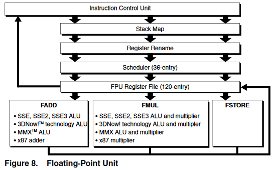
Execution units are 64-bit wide (or 80-bit, if you’re using x87), so 128-bit SSE vector operations are broken into two micro-ops. Still, vector and floating point throughput is better than Netburst’s, which also uses 64-bit execution units but only has one pipe that can handle FP/vector operations. Vector integer operations can use two pipes on K8, while they’re also restricted to a single pipe on Netburst.
AMD has better floating point execution latency as well. K8 can handle FP adds and multiplies with 4 cycle latency, while Netburst takes 5 and 7 cycles respectively.
Memory Execution (Load/Store Unit)
When any pipelined CPU handles a load instruction, it has to determine whether data should come from cache or an in-flight store instruction. This is done by comparing a load’s address against that of earlier stores in flight.
But thorough comparisons are expensive, and CPU designers will try to implement a fast path that covers the easiest, most common cases. Then, more difficult ones use a fallback path that probably involves waiting for the store to complete before executing the load, then reading the data from cache.
K8’s memory ordering check mechanism is extremely basic. Store to load forwarding requires exact address matches and 8-byte alignment. Netburst can handle all cases when addresses match, unless either access crosses a 64B cache line boundary. A failed store forwarding case usually takes about 10 cycles, but the penalty increases to 15 cycles if a 8 byte boundary is crossed. Even non-overlapping accesses see decreased throughput if they cross 8B boundaries. If store forwarding succeeds, latency is around 5 cycles on both Netburst and K8.
The biggest difference though, is Netburst’s massive penalties. Failed store forwarding costs 51 cycles, versus 10-15 on K8. Misaligned accesses require an extra cycle or two on K8, compared to 23-100 cycles on Netburst, depending on whether the misaligned access was a load or store.

K8’s memory ordering buffers also deserve mention, because it’s a pretty unique design. Most CPUs today have separate load and store queues. K8 has two unified queues. The first has 12 entries, and holds memory operations waiting to check the L1D cache. After operations in that first queue have probed the cache, they’re moved to the second 32 entry queue, where they wait for retirement.
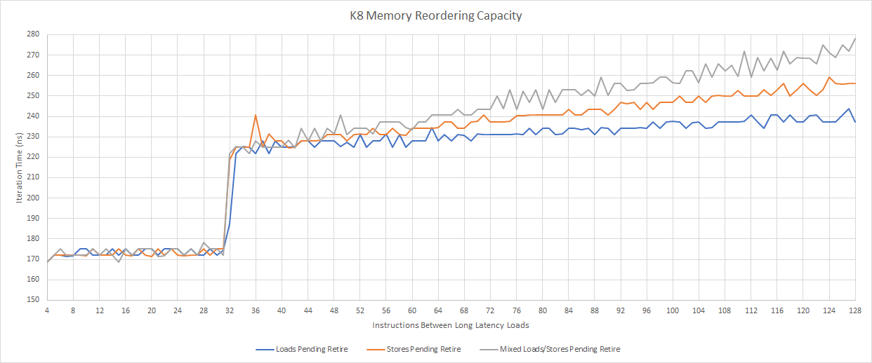
As far as reordering capacity goes, K8 can track up to 32 in-flight memory instructions, without separate limits for loads or stores. This flexibility lets AMD get by with fewer total queue entries in the load/store unit. But Netburst’s load and store queues are each larger than 32 entries, so AMD is at an unquestionable disadvantage here (unless Netburst has a batch of entries plugged up by bogus ops).
Cache and Memory Subsystem
To speed up data access, each K8 core has a 64 KB L1 data cache and a 1 MB L2. The L2 cache is a victim cache, and is exclusive of L1D contents. Since the L1 and L2 are both write-back caches, they feature ECC protection.
Latency
Thanks to the L1D’s impressive three cycle latency, the Athlon 64 FX-62 matches the Pentium Extreme Edition 965’s L1D latency despite running at lower clocks.

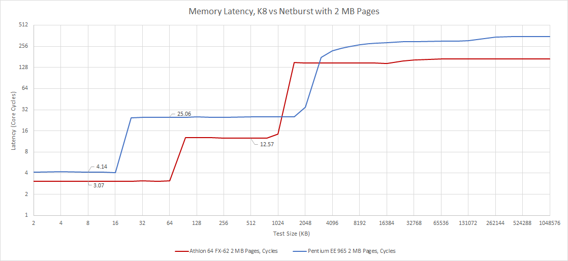
At L2, the situation is more interesting. K8’s L2 is smaller, but has much lower latency than Intel’s. On paper, AMD’s latency is even lower. Hot Chips slides for K8’s introduction suggest 11 cycle L2 latency, however we measured 12.5 cycles. I wonder if that only applies to variants with smaller L2 caches, since K8’s L2 cache size is configurable up to 1 MB.

When caches are missed, AMD’s integrated memory controller allows the Athlon to access DRAM with impressively low latency. 60 ns of raw memory latency is quite good even by modern standards. Netburst has to go through the motherboard chipset to hit DRAM, and suffers over 94 ns of latency. Intel’s latency disadvantage may have driven them to increase L2 cache size, since their memory accesses are far more expensive than AMD’s.
Client applications usually use 4K pages, since larger page sizes tend to waste memory and face issues with fragmentation. But tracking smaller pages means less TLB coverage, and thus higher address translation penalties.

Intel has a small advantage under 256 KB, thanks to a larger 64 entry DTLB. AMD’s K8 only has a 32 entry L1 DTLB, so address translation penalties bring its effective L2 latency closer to Intel’s as test sizes exceed 128 KB. But at larger test sizes, K8 can fall back on its 512 entry L2 TLB. In contrast, Netburst has nothing. There’s no L2 TLB, so Intel is eating 20+ cycle page walk penalties. In DRAM, page walk penalties get worse because the paging structures themselves can spill out of cache. K8’s memory access latency is almost half that of Netburst’s when testing with a 1 GB array.
Bandwidth
Cache bandwidth is not K8’s strong suit. Netburst’s wider datapaths and higher clocks give it a huge advantage. With SSE reads, K8 cannot match Netburst’s bandwidth at any level in the memory hierarchy. Agner’s instruction tables suggest K8 can actually achieve higher cache bandwidth using 64-bit scalar reads. 128-bit SSE reads (MOVDQA and MOVDQU) are broken into two 64-bit micro-ops that can only execute on the FSTORE pipe, resulting in a throughput of one 128-bit read every two cycles. Meanwhile, scalar 64-bit loads can execute every cycle using the three AGUs, limited by the dual ported data cache. That creates an awkward situation where bandwidth hungry vector code may end up with access to less cache bandwidth than scalar code, which typically cares more about latency than bandwidth.

But K8 does better once we hit memory and load both cores. AMD’s integrated memory controller and faster memory configuration mean memory bandwidth scales as both cores are loaded. Meanwhile, the Pentium Extreme Edition 965 actually loses DRAM bandwidth with all threads active, likely because of contention over the shared front side bus.

Write Bandwidth
K8 uses a write-back L1 data cache, so data written to L1D stays there until its evicted. With Netburst’s write-through L1D, data written to L1D is immediately written to L2 as well, meaning that write bandwidth is restricted by L2 bandwidth. I mentioned in the Netburst article that I don’t think the benefits of a write-through cache justify the drawbacks.

Thanks to Netburst’s L1D bandwidth being MIA as far as writes are concerned, AMD has a substantial write bandwidth advantage when test sizes fit in L1D. Intel has a small write bandwidth lead in L2, but loses again in DRAM.
Coherency Latency

Contended locks that require cross-core data movement are more expensive on Netburst, because all off-core communication goes through an external northbridge. K8 can handle core-to-core communication with its integrated northbridge, and thus enjoys lower latency.
K8 vs Netburst Breakdown

Final Words
AMD’s K8 architecture represents a very minor evolution over previous K7-based Athlons. The integer scheduling queues got a couple of extra entries each, TLB sizes were doubled, and the FP register file got extra entries to better handle SSE loads. But that’s about it. Reordering capacity, core width, branch prediction resources, and execution unit layout all stay the same. K8 feels like something between a “tick” and a “tock” in Intel’s tick-tock model.
Next to Netburst, K8 has low reordering capacity and is devoid of flashy microarchitecture features. Some parts of the core look absolutely primitive, like the store forwarding mechanism that requires 64-bit alignment to work. On paper, it should have no chance against Intel’s monster. But specifications can be misleading, and cool architecture techniques are no substitute for getting the basics right. That’s how K8 manages to stay competitive. It’s a forgiving architecture with mild penalties and low latencies. By conservatively iterating off a proven design and continuing to execute well on the fundamentals, AMD achieves higher IPC and stays competitive against Intel’s more advanced and innovative Netburst design.
Instead of pursuing drastic architecture changes, AMD focused engineering effort on extending the x86 instruction set to 64-bit and implementing system level changes. Work in both areas paid off. x86-64 went on to dominate consumer and server markets, with only a 2-3% die size increase compared to an “equivalent x86-32 implementation”. More importantly, x86-64 was a very straightforward extension of 32-bit x86 that minimizes instruction encoding differences. That made it easy to maintain compatibility and high performance with existing 32-bit code. Contrast this with ARM’s decision to drastically change instruction encodings (and much more) between 32-bit and 64-bit, which increased decoder complexity and meant they couldn’t afford to maintain 32-bit compatibility indefinitely, even with increasing transistor budgets.
K8’s new integrated memory controller gave reduced latency and higher bandwidth. And AMD’s HyperTransport enabled high bandwidth cross socket links, which is an important advantage in multi-socket servers. Throughout the mid 2000s, this careful allocation of engineering effort paid off and allowed AMD to go head to head against a much larger company.
But the original Athlon core was introduced in 1999. By 2006, the architecture was getting a bit long in the tooth. When Intel introduced Merom toward the end of that year, K8 needed more than a minor tweak to stay competitive.
If you like our articles and journalism and you want to support us in our endeavors then consider heading over to our Patreon or our PayPal if you want to toss a few bucks our way or if you would like to talk with the Chips and Cheese staff and the people behind the scenes then consider joining our Discord.