
Caching Energy Efficiency Data – Mobile and AVX-512

A few days ago, we looked at the power costs associated with moving data on some desktop parts. This is a short follow up with some data from Zen 3 and Willow Cove in mobile configurations, as well as Cascade Lake-X. That lets us dig into how power costs differ in mobile designs, and show how AVX-512 affects the picture.
Desktop vs Mobile Zen 3
AMD’s desktop “Vermeer” and mobile “Cezanne” platforms may use the same Zen 3 cores, but implement them in very different ways. Vermeer uses two CPU core chiplets and a separate IO die to provide lots of cores, cache, and IO at low cost. However, Vermeer’s setup is less optimized for power efficiency. Moving data between chiplets costs more power than doing so within a monolithic die. The IO die is fabricated on an older process. Firmware tunes the setup for maximum performance, achieving very high clocks under multi-core loads.
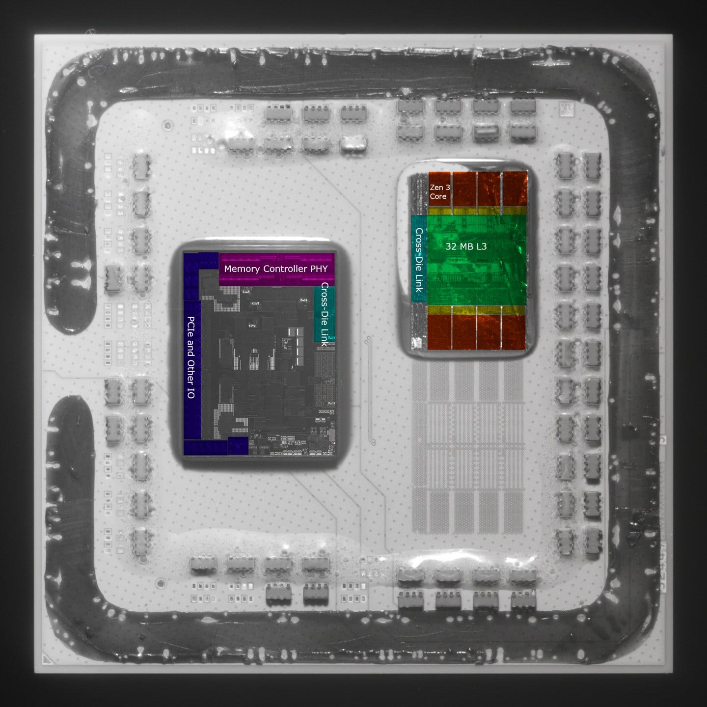
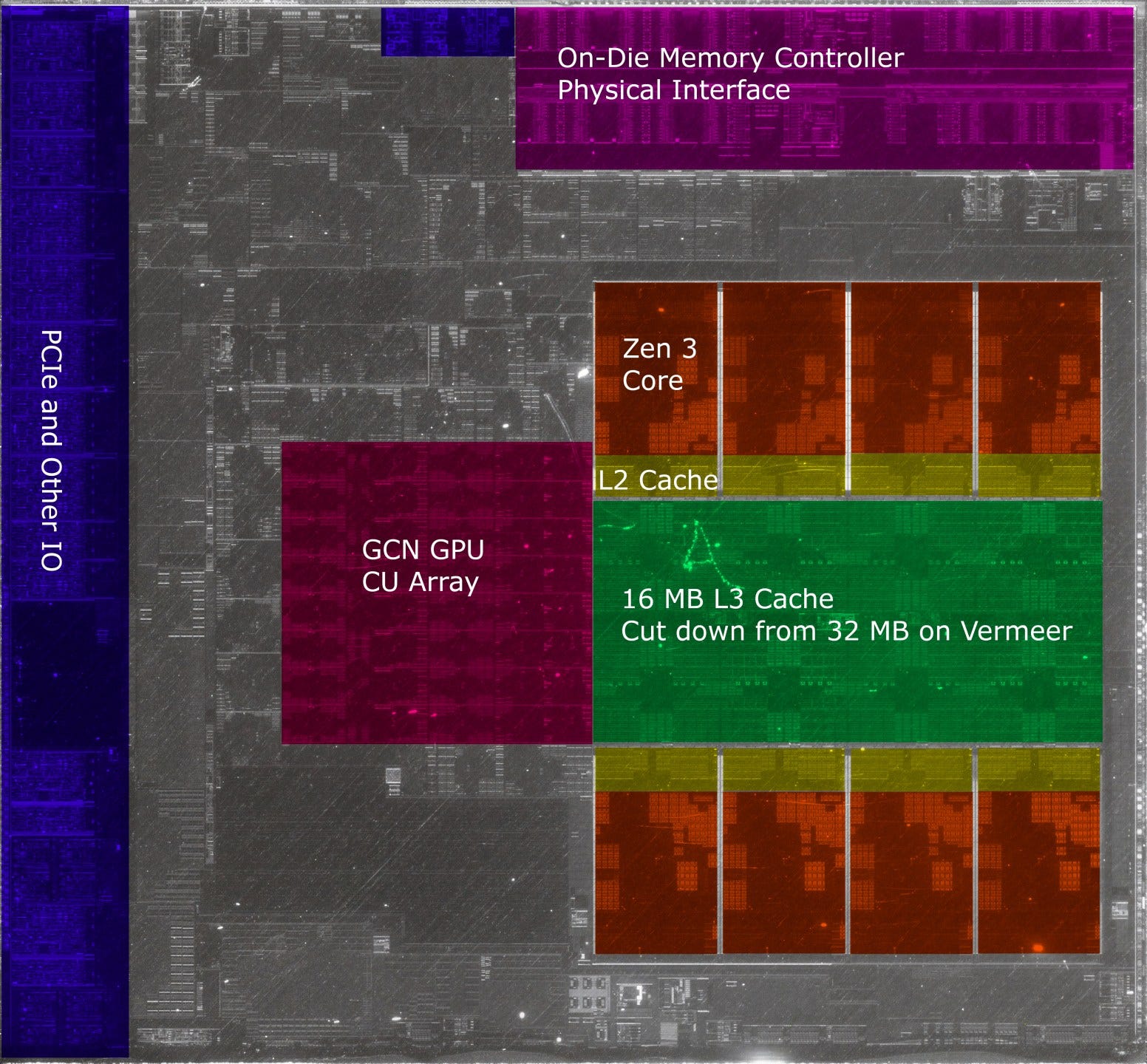
Cezanne opts for a monolithic die to keep power under control. It also integrates a relatively powerful iGPU that occupies a substantial amount of die area. So, Cezanne maxes out at eight Zen 3 cores, with half has much L3 cache per core as Vermeer. Cezanne is also set to a much lower power target, meaning that it’ll generally hit lower multi-core clocks than Vermeer.

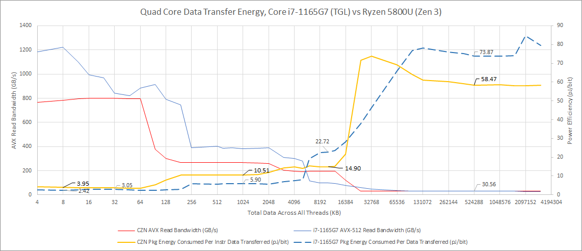
In our data transfer power test, the Cezanne-based Ryzen 7 5800U achieves much lower bandwidth per core than the Vermeer-based Ryzen 9 5950X. But it also moves data with far better power efficiency. If AMD’s power counters are accurate, it’s comparable to Tremont in some areas. Based on achieved L1D bandwidth, the Ryzen 7 5800U probably ran at around 3.1 GHz, while the Ryzen 9 5950X held a staggering 4.5-4.6 GHz with four cores active. Within the L1D region, the 5950X’s package power exceeded 90W, while the 5800U stayed around 25W.

The instruction side is similar. Cezanne is far more energy efficient. Differences are particularly staggering when going out to memory. When hitting cache, Vermeer benefits from “race to sleep” by finishing data movement faster, which means it’s not quite as inefficient as raw package power draw numbers would suggest. But that doesn’t apply for test sizes that spill into DRAM. Both chips are memory bottlenecked, and Vermeer’s drawing a lot more power while not being much faster.
Tiger Lake-U with Willow Cove
Sunny Cove never made a significant impact on the desktop scene. But Willow Cove had a decent presence in the mobile market for a couple years. Tiger Lake-U comes with a maximum of four Willow Cove cores per chip, though Intel has Tiger Lake-H45 with eight Willow Cove cores per chip. But that SoC has a different power profile. Like other Sunny Cove variants, Willow Cove features AVX-512 support, letting a single instruction load 64 bytes at a time – twice what Zen 3 can do with AVX. That gives it a substantial power efficiency advantage when reading from is core-private L1 and L2 caches while also providing higher bandwidth. AMD’s excellent L3 design still stands out though. In test sizes exceeding 1280 KB per core, AMD’s L3 provides higher bandwidth with better energy efficiency than Intel’s Tiger Lake-U. Finally, AMD holds a slight advantage when reading from DRAM.
There’s a twist to Willow Cove’s excellent energy efficiency here. From bandwidth figures, clocks probably started a bit above 2.3 GHz. Further into the test (but still within L1D test sizes), clocks dropped well below 2 GHz. These low clocks may have pushed Willow Cove closer to the core’s efficiency sweet spot. We previously saw that Intel’s core private caches were pretty good in Golden Cove. That trend may have started with Willow Cove.
From the instruction side, Tiger Lake-U / Willow Cove isn’t as impressive. It consumes more power per instruction fetched than Cezanne / Zen 3 at every level in the memory hierarchy.

So while Willow Cove might have excellent efficiency characteristics with vector code, particularly if AVX-512 is used, AMD might have an edge elsewhere. Drawing a conclusion is made harder because it’s not clear whether Tiger Lake-U was throttling as this test progressed. We know that Sunny Cove and its derivatives have enough micro-op cache capacity to sustain 5 IPC if loop size per core is under 4 KB with 4 B NOPs. Willow Cove shouldn’t see an instruction bandwidth decrease until after 16 KB (4 KB for four cores), but that’s what we see. From bandwidth figures, clocks likely dropped from almost 2.7 GHz to 2.3 GHz as the test moved from 4 KB to 16 KB (or, around 45 seconds of load).
AVX-512’s Effect
Previously, we saw Gracemont’s L1D achieving lower efficiency than Golden Cove’s, because accessing the L1D 128-bits at a time meant Gracemont was tracking twice as many accesses to move the same amount of data. In theory, AVX-512 should also provide an efficiency boost, and we do see Tiger Lake pull ahead of Cezanne in L1 and L2. But does this extend to 14nm as well?

With the Cascade Lake-based 10980XE, not really. It ends up slightly less efficient when pulling data from its L1D, even though it can use AVX-512 instructions to load 64 bytes at a time. Despite clocking a little lower than the i5-6600K, it looks like Intel’s HEDT platform just isn’t optimized for power efficiency. But we can’t ignore the gigantic 80%+ bandwidth lead Cascade Lake-X gets. It’s a bit less efficient, but that may be an acceptable tradeoff if you need the bandwidth.
At L2, Cascade Lake remains reasonably efficient considering its L2 is much larger than Skylake’s client derivatives (Kaby, Coffee, Comet). But in L3, Intel’s new mesh setup is a letdown. Bandwidth is nothing to write home about, and we’re seeing 80 pJ used per bit of data shortly after spilling out of L2. L3 performance also isn’t a redeeming factor. We see just 138.72 GB/s with 8 MB of data across all four threads. For comparison, four Zen 3 cores in the 5950X can get 438 GB/s out of L3 with the same amount of data in play, while using less than half as much energy per bit.
Rocket Lake
But Cascade Lake is just one example. Another is Rocket Lake. It uses a Sunny Cove core derivative called Cypress Cove, that was backported to 14nm and targeted very high clocks. The best point of comparison I have is Kaby Lake. It also targets high clocks, and as a result, loses a bit of efficiency compared to 6th generation Skylake.

In core private caches, we’re splitting hairs. Kaby Lake needs about 9.8% more power per bit in L1, and about 2.2% less in L2. But this is still a win for AVX-512, because Rocket Lake is able to get more than twice as much bandwidth out of L1 and L2 at roughly the same energy efficiency. In L3, AVX-512 doesn’t matter anymore. AVX is enough to max out L3 bandwidth, so Rocket Lake isn’t getting any “race to sleep” benefits. Also, Rocket Lake has a longer ring bus and more L3 capacity, which would increase power consumption and hurt its energy efficiency.
Final Words (Mobile)
Desktop parts are often pushed way past their best efficiency points in pursuit of high performance. We saw that when testing general application performance, and the same applies when microbenchmarking data transfer efficiency.
Mobile parts are different. Battery life and thermal constraints force them to pick a different balance, even if the same cores are used. AMD uses very different designs at the chip level, ditching the chiplet setup to get the power benefits of a monolithic die. Both manufacturers do firmware tuning to keep package power under a certain level. That prevents heat output from overwhelming the laptop’s cooling system. In this example, firmware on the Intel platform also opted to gradually pull back clocks under a quad-core load, while the AMD one opted to keep clocks mostly constant.
That’s also why deep diving CPU architectures with mobile CPUs is hard. Unlike desktops, mobile platforms generally aren’t set up to indefinitely sustain multi-core loads at maximum boost clocks. That causes lack of clock stability during a test run, which complicates result analysis. In the end, there’s a real risk laptop OEM decisions influence test results just as much as CPU architecture. Thankfully, throttling on Tiger Lake-U doesn’t seem to dramatically change the power efficiency picture. But that’s why I initially left laptop data out of the previous article.
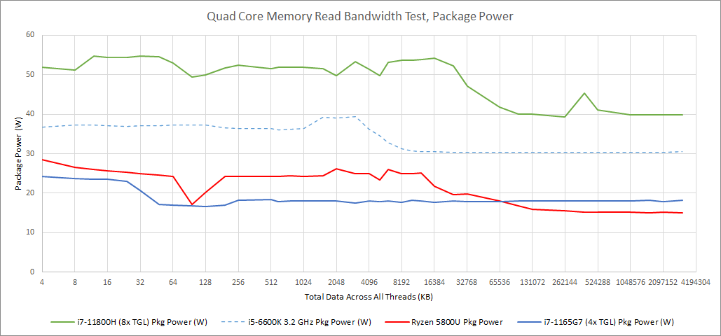
As you can see above, a desktop chip has pretty steady power draw (35-40 W) during the test run. Power only decreases when test sizes exceed cache capacity, and cores are spending a lot of time waiting for data. In contrast, mobile chips may start with high power draw that they don’t sustain. That’s particularly apparent with the i7-1165G7, which wanted to stay well below 20W with a sustained quad-core load. The i7-11800H is a counterexample. It had a 55W PL2 (short duration power limit), which let it stay above 4 GHz.
But despite the limitations of testing on laptops, hopefully this data provides some interesting perspective on how mobile and desktop parts differ, even if they use the same CPU cores. AMD’s chiplet design has let them deliver high core count at low cost, but high non-core power consumption forces a very different solution on mobile. And both CPU makers run far lower multi-core boost clocks on mobile. All of that means data transfer power efficiency in mobile designs is a lot closer to that of low power cores than their desktop cousins.
Final Words (AVX-512)
Intel has a long tradition of leading the pack with L1D vector bandwidth. Netburst’s L1D could handle full-width 128-bit SSE loads while AMD’s Athlon broke them into two 64-bit micro-ops. Sandy Bridge natively handled 256-bit AVX loads when AMD’s Bulldozer split them into 2×128-bit ops. Today, every AVX-512 capable Intel CPU can natively do 512-bit L1D accesses, while AMD’s current CPUs don’t have AVX-512 support and max out at 256-bit. In theory, AVX-512 could improve L1D energy efficiency, because half as many accesses are needed to transfer the same amount of data compared to AVX. That also means fewer address calculations, tag checks and instructions retired.
Of course, reality is complicated, and it’s hard to get a head to head comparison. Tiger Lake beats mobile Zen 3 while being more efficient. But Zen 3 is also a very different architecture that doesn’t have an edge against Golden Cove when AVX was used for both CPUs. Cascade Lake wound up behind client Skylake in terms of L1D efficiency, but Cascade Lake aims for much higher power targets than client Skylake. Rocket Lake strangely ends up being the clearest example of AVX-512’s efficiency, when compared to Kaby Lake. Both CPUs are implemented on similar process nodes, but Rocket Lake delivers much higher L1D bandwidth with slightly better efficiency.
Still, that’s enough to show AVX-512’s efficiency potential. Intel in general is very strong with vector workloads, and data transfer efficiency with wide vectors is part of it. Of course, the pool of applications that can take advantage of AVX-512 is still small. But as adoption grows, Intel’s AVX-512 capable CPUs could see efficiency gains.
If you like our articles and journalism and you want to support us in our endeavors then consider heading over to our Patreon or our PayPal if you want to toss a few bucks our way or if you would like to talk with the Chips and Cheese staff and the people behind the scenes then consider joining our Discord.