AMD’s Ryzen 9950X: Zen 5 on Desktop
AMD’s desktop Zen 5 products, codenamed Granite Ridge, are the latest in the company’s line of high performance consumer offerings. Here, we’ll be looking at AMD’s Ryzen 9 9950X. We already saw most of what Zen 5 looked like in Strix Point, so this article will focus on the differences between AMD’s mobile and desktop Zen 5 cores. With a higher power budget and no die area wasted on a NPU, desktop Zen 5 gets more cache, a beefed up FPU, and higher clock speeds.
Acknowledgments and Testing Notes
We’d like to thank AMD for getting us a sample before release date as well as we would like to thank our Patreons and folks who donate to Chips and Cheese without whom we would not have been able to get a X670E board or DDR5 memory for testing.
The Ryzen 9 9950X was tested using a Gigabyte X670E Aorus Master, with G.SKILL F5-6400J3239F48G DDR5 memory. Tests were run with memory speed set to 6000 MT/s, since AMD’s reviewer guide suggests that’s the sweet spot.
System Level
AMD’s Ryzen 9 9950X uses a chiplet setup that’s been a staple of AMD desktop chips since Zen 2. Two Core Complex Dies (CCDs) connect to an IO die, which contains memory and PCIe controllers along with other IO. Of course, AMD has made improvements between each generation, and those carry forward to the 9950X. Each CCD on the 9950X has eight Zen 5 cores and 32 MB of shared L3 cache, a baseline inherited from Zen 3. The IO die is carried forward from Zen 4, giving the Ryzen 9950X a tiny iGPU and DDR5 support. AMD’s Infinity Fabric interconnect ties all those on-chip blocks together.
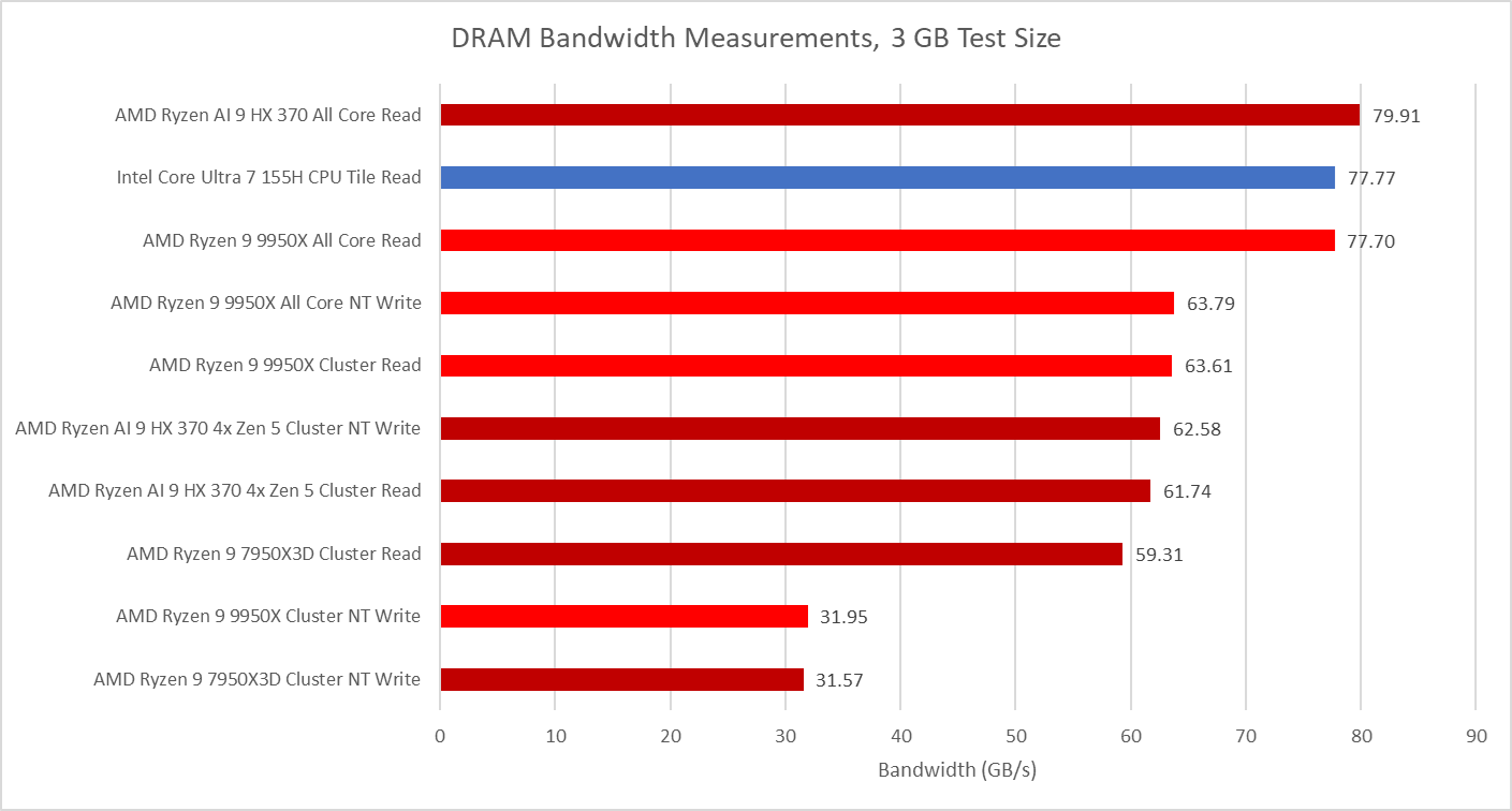
As with Zen 2, each CCD connects to the IO die through an Infinity Fabric link. On desktop, this link is 32 bytes per cycle in the read direction and 16 bytes per cycle in the write direction. That differs from AMD’s mobile parts, where the Infinity Fabric link from a core cluster can do 32 bytes per cycle in both directions. Infinity Fabric runs at 2 GHz on both setups, just as it did on desktop Zen 4. That’s not a surprise, since AMD has re-used Zen 4’s IO die for Zen 5. At that clock speed, each cluster has 64 GB/s of read bandwidth and 32 GB/s of write bandwidth to the rest of the system.
Those per-cluster bandwidth limits are exactly the same as in desktop Zen 4. However, the Ryzen 9 9950X gets closer to Infinity Fabric’s theoretical limits, possibly because it’s using a faster DRAM setup.
With both clusters loaded, the Ryzen 9 9950X achieves about as much memory bandwidth as Intel’s Core Ultra 7 155H. That’s impressive because the 155H uses LPDDR5-7467, which offers 119.47 GB/s of theoretical bandwidth compared to the Ryzen 9 9950X’s theoretical 96 GB/s. AMD’s own Strix Point mobile APU achieves slightly more bandwidth from its own LPDDR5 memory controllers, but its bandwidth advantage is small.
Standard DDR5 really shines in offering better latency, and that’s the case on Ryzen 9 9950X. It’s better than the Ryzen 9 7950X3D with DDR5-5600, and much better than LPDDR5 in mobile setups. XMP / EXPO was enabled on both the Zen 4 and Zen 5 system. Do note that XMP / EXPO is technically considered overclocking, though enabling XMP / EXPO is common practice on enthusiast systems. Memory setups were not matched because Cheese has the Zen 5 setup, and I (Clam) live in a different area. Therefore, my focus is on AMD’s architecture changes, with absolute performance differences taking a back seat.
New memory technologies often come with higher bandwidth, but latency is often sees little improvement or even a regression. With just over 70 ns of memory latency, the Ryzen 9 9950X with DDR5-6000 is just about able to match a Core i7-4770 with DDR3-1333. Zen 5 has much more reordering capacity and better caching, making it more latency tolerant than Haswell. The combination of low latency and improved architecture is a great combination to see.
Core to Core Latency
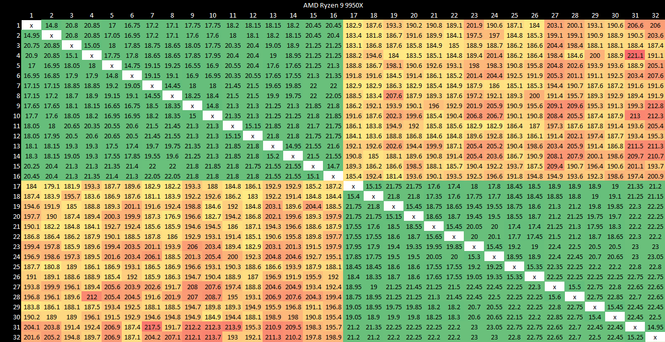
Multi-core CPUs have to ensure all of their cores see a coherent view of memory. That’s a little challenging because each core has its own private caches. If one core wants to read data written by another, the CPU’s interconnect has to do a cache to cache transfer. While such operations are relatively uncommon compared to regular L3 misses, it’s cool to see just how they perform by bouncing a cacheline between core pairs.
Zen 5 continues to enjoy very fast cache to cache transfers within a cluster. However, cross-cluster latencies are high compared to prior generations. At nearly 200 ns, cross-cluster latencies aren’t far off from cross-socket latencies on a server platform. It’s a regression compared to prior Zen generations, where cross-cluster latencies were more comparable to worst-case latencies on a monolithic mesh based design.
The Ryzen 9 7950X3D for example typically completes cross-cluster cache transfers in less than 80 ns.
Clock Speed
The Ryzen 9 9950X’s two CCDs exhibit clock behavior that’s similar to prior generations. One CCD clocks up to 5.72 GHz, while the other maxes out at 5.49 GHz. Compared to prior generations though, the clock speed difference is minor. There’s no preferred core within a cluster, suggesting silicon quality variations are less of an issue. This uniform behavior should ease the burden on operating system thread scheduling.
Maximum clock speeds are nearly unchanged compared to the prior generation Ryzen 9 7950X. Zen 4 already had very little boost clock variation within each die, and Zen 5 cuts that down further. Boost clocks are hit very quickly on the Ryzen 9 9950X. Cores from both dies reach their maximum clocks in less than a millisecond.
Decode Clusters, and SMT On/Off
Zen 5’s frontend has a 8-wide decoder, arranged in two 4-wide clusters. It’s AMD’s first clustered decode implementation, and differs from clustered decode in Intel’s E-Cores in that a single thread appears unable to use both decode clusters together. The Ryzen AI 9 HX 370 laptop didn’t have an option to turn off SMT in the BIOS, but the Gigabyte X670E Aorus Master does.
Disabling SMT at the BIOS level is interesting because the process of transitioning a core between 1T and 2T mode feels complex from a layman perspective. A large number of core resources need to be reconfigured when a core switches between 1T and 2T mode. Doing so almost certainly involves stalling the already running thread until enough entries in core structures have been freed up. In the example above, the reorder buffer (ROB) is a statically partitioned resource when both SMT threads are active. When the thread 1 wants to start running code, the renamer would need to stop sending new instructions for thread 0 into the backend until thread 0’s ROB utilization drops to 224 or fewer entries.
It is expensive to transition between single-threaded (1T) mode and dual-threaded (2T) mode and vice versa, so software should restrict the number of transitions
Software Optimization Guide for AMD Family 17h Processors (Zen 1)
But stalling can’t happen for too long. Operating systems might do dumb things like repeatedly scheduling a low priority background process on the same core that a high priority game thread is running in. 1T to 2T transitions have to happen quickly. Maybe such a transition with a Tremont-style out-of-order decode scheme was too expensive, or too difficult to pull off with acceptable performance impact.
Disabling SMT in the BIOS should mean the second SMT thread is never initialized. In that case, the core should never have to worry about 1T/2T mode transitions, and could hypothetically use both clusters for the same thread. But that doesn’t happen.
Frontend bandwidth is identical regardless of whether the core is running with SMT off, or with SMT on and one thread active. Once code spills out of the micro-op cache, fetch bandwidth drops to four 4-byte NOPs per cycle. As with mobile Zen 5, using both SMT threads together brings total fetch bandwidth to 8x 4-byte NOPs per cycle.
At this point, I have to guess at why Zen 5’s clustered decode is geared towards running with both of a core’s SMT threads active. Zen 5, like pretty much any recent CPU, comes with a rich set of performance monitoring events. Among other things, Zen 5 can track where it sourced micro-ops that were sent to the backend. Setting unit masks for the micro-op cache and x86 decoder sources indicate Zen 5’s micro-op cache is large enough to cover the majority of the instruction stream across quite a few applications.

If both SMT threads are active, micro-op cache hitrate tends to drop as the two threads compete for cache capacity. Performance counters of course can also track retired instructions and active thread cycles. Checking those indicates a single thread rarely pushes up against 4 IPC. And as we’ll see later, some of the lower IPC examples here are more limited by latency than bandwidth.
With both SMT threads active, sustaining more than 4 IPC looks like a more common case. Tracking per-core IPC with both SMT threads active is unfortunately very difficult because Zen 5 doesn’t have a performance event that counts when either SMT thread is active. But many of these applications can load the majority of logical threads its given, and doubling per-SMT-thread IPC can give an upper estimate.
There’s no way to know why AMD implemented clustered decode in this way unless their engineers state why. But my guess is it’s for the following reasons:
Higher decode bandwidth is useful when micro-op cache hitrate decreases, which happens when both SMT threads are in use. Conversely, a single thread benefits less from two decode clusters because it’s more often running out of the micro-op cache.
Higher decode bandwidth is more advantageous when IPC is not limited by latency, which happens when both SMT threads are in use. Conversely, a single thread is often latency limited and stands to gain little from wider decode
Locking one thread to one decode cluster may simplify and speed up SMT mode transitions, and avoids having to tag queue entries in each decode cluster with a thread id.
Zen 5’s decode clusters are superficially similar to those on Intel’s E-Cores, but we have to account for Zen 5’s different design when judging the frontend implementation. Intel’s E-Cores use their decoders as the only method of instruction delivery and don’t have SMT. Therefore, clustered decode is used to accelerate instruction delivery for a single thread as an alternative to using a micro-op cache. Zen 5 accelerates instruction delivery with a micro-op cache, and its hitrates are high enough to let it act as the primary mode of micro-op delivery. Zen 5’s dual decode clusters are mainly used to improve SMT performance, where micro-op cache hitrate is lower and potential per-core IPC is higher.
Cache Setup
Desktop Zen 5’s cache setup is nearly identical to Zen 4’s, except for the larger data cache. That’s largely a good thing, because Zen 5 inherits the low latency L3 from prior generations. Compared to mobile Zen 5, the desktop version gets a full 32 MB of L3 cache. Add lower DRAM latency into the mix, and Granite Ridge has a much stronger memory subsystem than Strix Point.
Bandwidth improves too. Desktop Zen 5 can do two 512-bit vector loads per cycle, up from one per cycle in Zen 4 and mobile Zen 5. Each Zen 5 core therefore enjoys very high L1D bandwidth. Intel was previously the champion here. Intel’s Golden Cove, first released in the Core i9-12900K, could do 2×512-bit vector loads. But the fun didn’t last long because Intel disabled AVX-512 in favor of going all-in on their mixed architecture hybrid strategy. Golden Cove derivatives like Redwood Cove still packed a lot of L1D bandwidth because they could do three 256-bit loads per cycle. But Zen 5 now leaves Intel in the dust.
L3 bandwidth was already very high in prior Zen generations, and Zen 5 improves even further. A single core can just about saturate its 32 byte per cycle interface to L3.
For a shared cache like Zen 5’s L3, bandwidth demands go up when more cores are in use. Again AMD does well, and Zen 5’s L3 bandwidth advantage persists with all cores in a CCD loaded up. Zen 4’s 852.3 GB/s was already nothing to sneeze at, and Zen 5’s 1.4 TB/s is even higher.
With all cores loaded, the Ryzen 9 9950X has over 10 TB/s of L1 data cache bandwidth. It’s a massive increase over prior generation consumer chips, including Intel’s Core i9-14900K. Intel’s chip has 24 cores to AMD’s 16, but sixteen of those are Gracemont efficiency cores with less cache bandwidth on tap. Even with a hybrid-aware test, Raptor Lake’s cache bandwidth is far behind.
Overall, Zen 5’s cache subsystem looks solid. AMD took an already good cache hierarchy, improved it, and didn’t try to fix what wasn’t broken.
AVX-512 Implementation
AMD has historically approached ISA extensions in a conservative manner, and vector extensions are a prominent example. Athlon chips handled 128-bit SSE instructions as two 64-bit micro-ops all the way until Phenom launched in 2007. AMD kept native 128-bit execution until Zen 2 hit the market in 2019. Zen 4 somewhat bucked this trend by handling 512-bit operations with a single micro-op with a notable exception for stores.
Zen 5 bucks that trend further, and adopts a split approach to AVX-512. Desktop Zen 5 uses its higher power and area budget to pursue a more aggressive AVX-512 implementation, while the mobile variant uses a more conservative approach. Compared to mobile Zen 5, desktop Zen 5 differs in the following ways:
All vector register file entries are 512 bits.
FP units have full 512-bit vector width
FP adds execute with 2 cycle latency, down from 3 cycles in Zen 4 and mobile Zen 5
Data cache can handle 2×512-bit loads per cycle. Zen 4 and mobile Zen 5 can only do one 512-bit load per cycle
Mask register file may have a few more entries on desktop Zen 5
Those changes make Zen 5 a force to be reckoned with for AVX-512 workloads. When covering Strix Point, I missed a small detail where AMD moved the vector rename stage to after the non-scheduling queue (NSQ). I think that’s an excellent optimization.
Micro-ops in the NSQ don’t need a vector register allocated for them because they can’t be considered for execution, and anything that needs their result also can’t execute because the NSQ is still in-order. In combination with doubling vector register file capacity, letting 96 vector/FP ops sit in the backend without a vector register allocated basically deletes dispatch stalls due to vector register file capacity.
One area that hasn’t seen major improvement is the store queue. Its entries are still 256 bits wide, and 512-bit store instructions take two entries. Moreover, performance counters indicate 512-bit stores are decoded into two micro-ops. At Hot Chips last year, AMD mentioned widening store queue entries to 512 bits would have been too expensive, and that appears to hold true today. However, Zen 5 did grow the store queue from 64 to 104 entries. Desktop Zen 5 also has an optimization where consecutive stores to the same cacheline only take one store queue entry. That could economize store queue entry usage for writes that don’t operate on 512-bit vectors, leaving more entries free for 512-bit stores.
Checking AVX-512 Gains
Daniel Lemire has AVX-512 code written to convert integers to strings, along with a simple table lookup approach for comparison. It’s a cool example to use for checking AVX-512 gains.
Desktop Zen 5 posts greater gains than its mobile counterpart. Intel traditionally tried to get the most out of new instruction set extensions, but now AMD is ahead with AVX-512. Even against Golden Cove with AVX-512 enabled, Zen 5 sees better gains and better absolute performance. Mobile Zen 5’s more conservative implementation still looks very strong compared to Zen 5, and looks like a good fit for lower area and power budgets. It’s about in line with Intel’s Ice Lake, which had a strong AVX-512 implementation for the time.
Zen 5’s Pipeline, in Practice
I already covered Zen 5’s core architecture in a prior article. Observations there largely apply to desktop Zen 5 as well, so it’s more productive to see how Zen 5’s architecture works when faced with a couple of workloads. I’m testing with a single CCD, with one SMT thread loaded per core. On the Ryzen 9 9950X, I’m using the higher clocking CCD. On my Ryzen 9 7950X3D, I’m checking both CCDs to see the effect of more L3 capacity. Clock speeds are not locked, unlike in my prior article on Zen 4’s VCache implementation. Boost is enabled, and both CPUs are running at stock.
libx264 does software video encoding, which offers better quality and storage space tradeoffs than hardware encoders. As a tradeoff, software encoding is more computationally heavy.
Right away, Zen 5 posts a good 27.6% performance uplift. Performance counters indicate the IPC uplift is 22.2%, comfortably above AMD’s claimed 16% average. libx264 likely sees better gains than average because it uses AVX-512 and has plenty of vector instructions. Zen 5’s beefy FP/vector unit can really shine here. Zen 4’s VCache variant enjoys higher IPC because higher cache capacity reduces the impact of memory latency, so Zen 5 only gets a 14.4% IPC gain there. However, VCache loses overall because its higher IPC is not enough to compensate for lower clock speeds.
Performance counters can help break down how a CPU’s core width is utilized. Zen 4 and Zen 5 can account for that at the slot level, giving reasons for why a pipeline slot was left unused. Analysis starts at the rename stage because it’s the narrowest part of the pipeline on both cores. “Retiring” here refers to pipeline slots that were actually used by retired instructions, and can be seen as core width utilization.
Other categories explain why core width was not used:
Backend memory bound: Instruction retirement was blocked by an incomplete load from memory. That includes cache latency at all levels, as well as DRAM latency. This is expressed as a percentage of pipeline slots lost because a backend resource was full.
Backend core bound. Retirement was blocked because of an incomplete instruction that’s not a load. Also expressed as a percentage of pipeline slots lost because a backend resource was full.
Frontend bandwidth bound: The frontend sent some micro-ops to the renamer, but not enough to fill all available slots.
Frontend latency bound: The frontend left all renamer slots empty during that cycle
Bad speculation: Renamer width was utilized, but those micro-ops were never retired. That means they were cancelled and flushed out because the frontend went down a path that ultimately shouldn’t have been executed.
libx264 is largely backend bound, and much of that can be attributed to cache and memory latency. Throughput lost to execution latency or frontend inefficiencies play a more minor role. At first glance, Zen 4 makes more efficient use of its core width than Zen 5, especially on the VCache variant. But that’s not a completely fair comparison because Zen 5 is wider, and extra core width is harder to utilize.
Not normalizing for core width gives a better perspective. Zen 5 is able to utilize more pipeline slots on average. On top of that, Zen 5 tended to have fewer micro-ops per instruction. Dividing micro-ops by instructions gives 1.028 for Zen 5, and 1.047 for Zen 4. Both architectures see little micro-op expansion, with the vast majority of instructions mapping to a single micro-op. But Zen 5 is just a little bit better.
Backend
If any backend resource fills up, the renamer stalls and core width is left unused. Therefore, CPU designers have a challenging optimization problem where they try to give each resource enough entries to prevent it from holding back reordering capacity, but not so large that it eats unacceptable power and area.
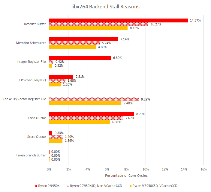
Zen 5’s biggest stall reason is the ROB filling up, which is a good thing because it suggests other resources are appropriately sized. AMD’s revamped NSQ setup deserves credit for basically eliminating stalls due to lack of FP/vector register file entries, an issue that Zen 4 struggled with. On the other hand, Zen 5’s integer register file only got a small capacity increase, and frequently finds itself full.
Higher reordering capacity is one way to mitigate backend stalls. The other is to reduce latency via better caching. Zen 5 increases L1 data cache capacity by 50%. Compared to Zen 4, demand L1D misses per instruction went down by 12.8%, which is nice to see. Both Zen generations satisfy the vast majority of L1D misses from lower cache levels. That’s great, but DRAM still plays a major role because each DRAM access costs hundreds of cycles.
Zen 4 and 5 can sample L3 misses and track their latency. That sampling only accounts for latency from the point of a L3 miss, which excludes time taken to check upper cache levels. A software latency test would include the latter. Estimating latency to the point of a L3 miss is impossible from software, but adding L3 hit latency to results seem to closely approximate latency as seen by software.
Average latency is well under 100 ns. Because latency dramatically increases as software starts approaching bandwidth limits, Infinity Fabric and DRAM bandwidth are not significant factors. Strix Point’s wider 32B/cycle Infinity Fabric write link and higher bandwidth LPDDR5 setup don’t matter, while LPDDR5’s higher base latency does.
Compared to Zen 4, the faster DDR5-6000 memory used on Zen 5 continues to offer better latency. The VCache Zen 4 die is only a bit behind, perhaps because higher cache hitrate lower bandwidth demands.
Frontend
A CPU’s frontend is responsible for bringing instructions into the core. libx264 isn’t particularly frontend bound, but it’s fun to look anyway. Frontend latency accounts for most lost throughput. L1 instruction cache and iTLB misses were relatively rare, so branch predictor delays likely account for those stalls.
Zen 5’s giant BTBs almost completely eliminate cases where the decoder discovers a branch and redirects the frontend from there. However, Zen 5 does see a lot of overrides from a second level branch predictor structure, or the indirect predictor. Indirect branches can go to more than one target, adding an extra level of prediction difficulty. Prior Zen CPUs handled indirect predictions at L2 BTB latency. I’m not sure how fast Zen 5 is with indirect branches, but if it works like prior Zen CPUs, that could explain the frontend latency bubbles.
From Zen 4 to Zen 5, AMD slightly shrank the micro-op cache from 6.75K entries to 6K entries. To compensate, associativity increased from 8-way to 16-way. That change seems to have gone well, with basically no difference in micro-op cache hitrate despite the lower capacity. AMD also deleted Zen 4’s loop buffer functionality. The loop buffer never made a lot of sense to begin with because the op cache already provided more than enough frontend bandwidth, and a 144 entry loop buffer wasn’t enough to capture a significant part of the instruction stream anyway.
Linux Kernel Compile, tinyconfig
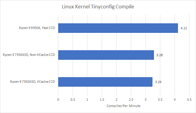
Code compilation can also be a time consuming workload. Here, I’m building the Linux kernel with the minimal tinyconfig configuration. That helps provide as much of an apples-to-apples comparison as possible by excluding system specific options. Unlike libx264 encoding, this workload doesn’t heavily exercise the vector units.
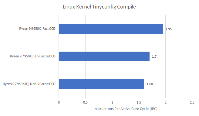
Zen 5 again pulls ahead by a comfortable margin, completing the compile job 25-27% faster depending on which Zen 4 CCD you’re comparing against. IPC gains are 14.7% and 21.8% against the VCache and non-VCache Zen 4 CCDs, respectively. Again, the VCache CCD’s higher IPC does not balance out its lower clock speeds. It’s a reminder that higher IPC is not always a winning approach.
From a top-down view, the most significant source of lost throughput is now frontend latency. Frontend bandwidth is an issue too, as is backend memory access latency.
Not normalizing for core width again shows Zen 5 is able to use more pipeline slots, even though it’s using a lower percentage of core width compared to Zen 4.
Still, a lot of potential throughput is left on the table due to memory latency and frontend delays. Let’s start with the frontend.
The branch predictor sits at the start of the frontend’s pipeline, and is a bit more accurate in Zen 5. Still, Zen 5 loses more pipeline slots to bad speculation than Zen 4, likely because it’s able to speculate further.
Micro-op cache hitrate is lower than with libx264, but hitrate is still high enough that it’s acting as the primary source of instruction delivery. Zen 5’s micro-op cache provides slightly better coverage of the instruction stream than Zen 4’s, again showing AMD’s micro-op cache changes were well informed.
While frontend latency creates serious issues for both cores, Zen 5’s improvements do pay off. A larger 16K entry L1 BTB means Zen 5 only suffers L2 BTB latency about 1/4 as often as Zen 4. Going from a 1.5K entry L1 BTB to a 16K entry one feels like beating a mosquito with a sledgehammer, but I can’t argue with the results. Decoder overrides happen when the branch predictor isn’t tracking a branch at all, so the decoder has to do a rather late (and costlier) override when it discovers a branch. Zen 5 cuts decoder overrides by by more than half, so the extra 8K entries provided by the L2 BTB are making an impact.
Address translations can add latency just like with data-side accesses. Zen 5 has to get translations from its L2 iTLB quite often. The larger L2 iTLB does cut down on expensive page walks, which is appreciated.
Even though backend stalls aren’t as severe as with libx264, a quick look does show Zen 5’s backend resources are less well distributed for this workload. The integer register file doesn’t have enough capacity and often causes stalls before ROB capacity is reached.
Zen 5’s more unified integer and memory schedulers also don’t do do as well, filling up a bit more often than on Zen 4. I’m not sure why that’s the case. Individual unit masks indicate the integer scheduler filled 3.6% of the time, while the AGU scheduler filled 1.3% of the time. Zen 4 can use up to 96 scheduler entries for ALU operations, while Zen 5’s integer scheduler only has 88 entries. Perhaps Zen 4’s setup is better in this case.
On the plus side, Zen 5 increases the taken branch buffer’s capacity from 62 to 96 entries. It’s a big increase, and basically removes the taken branch buffer as a stall reason. Zen 4 didn’t suffer much, but any improvement is appreciated.
Comments on Zen 5’s Core Architecture
From these two workload examples, Zen 5’s architecture changes are mostly well informed. AMD has addressed limiting factors in Zen 4’s backend like FP register file and store queue capacity. At the frontend, larger BTBs and a huge L2 iTLB help attack latency. But addressing one limitation inevitably reveals another. For Zen 5, the integer register file is often the next limitation.
At the top level, the picture is largely unchanged between Zen 4 and Zen 5. Latency, both in the frontend and with backend memory accesses. Zen 5 is less core bound and has more frontend bandwidth, but those weren’t the biggest limitations anyway. That’s probably why AMD kept the Zen line 5-6 wide for a long time. I suspect a good portion of Zen 5’s performance gains come from a combination of lower latency memory and more reordering capacity, rather than higher core width.
Final Words
AMD deserves credit for how fast they’ve been able to iterate. Since Golden Cove launched in 2021, AMD has released Zen 4 and Zen 5. Both bring significant architecture changes. On Intel’s side, Raptor Cove reuses Golden Cove cores at higher clock speeds with more cache. Redwood Cove does have smattering of minor improvements like more aggressive prefetching, a larger micro-op queue, and doubled L1i capacity. But major structure didn’t see layout or capacity changes, so Intel’s changes have minor impact compared to AMD’s. And Zen 5’s improvements can be quite impressive in areas once dominated by Intel, like AVX-512.
As for AVX-512, AMD’s engineers didn’t stop at creating one strong FP/vector unit. Instead, they designed, optimized, and validated two versions of it to better fit mobile and desktop requirements. That was done alongside implementing the core in performance and density optimized variants. Add on significant core changes, and it’s clear Zen 5 took a lot of engineering bandwidth. For sure, AMD still economizes engineering effort by reusing Zen 4’s IO die and not maintaining two completely different core architecture lines as Intel does. But AMD today feels more ambitious and capable than it was in 2017.
But any engineering team has limits, and compromises are inevitable considering how fast AMD is pushing out cores. Zen 5’s integer register file didn’t get large enough. Clock speed increases are minor compared to prior generations. AMD’s first clustered decode implementation can’t have both clusters work on a single thread. Widening the core may have been premature too. Much of the potential throughput offered by Zen 5’s wider pipeline is lost to latency, either with backend memory accesses or frontend delays.

Fortunately, some of those compromises have little impact. 4-wide decode likely isn’t a limiting factor for single threaded performance, thanks to high micro-op cache hitrates and other limiting factors coming first. Minimal clock speed gains are paired with lower power consumption. And when paired with faster memory, the Ryzen 9 9950X can comfortably beat the Ryzen 9 7950X3D in productivity workloads.
As a foundation, Zen 5 looks solid and I’m excited to see how AMD builds on it in the future. I’m also looking forward to VCache-enabled Zen 5 variants. Increasing L3 capacity from 32 to 96 MB on Zen 3 and Zen 4 did wonders for certain games. Its largest issue was losing clock speeds, which made it a hit or miss affair on other programs. If Zen 5 can keep clocks up, a VCache variant that loses less core width to memory latency could be a force to be reckoned with.
Again, we would like to thank AMD for sending us over some Zen 5 CPUs for review and if you like our articles and journalism, and you want to support us in our endeavors, then consider heading over to our Patreon or our PayPal if you want to toss a few bucks our way. If you would like to talk with the Chips and Cheese staff and the people behind the scenes, then consider joining our Discord.











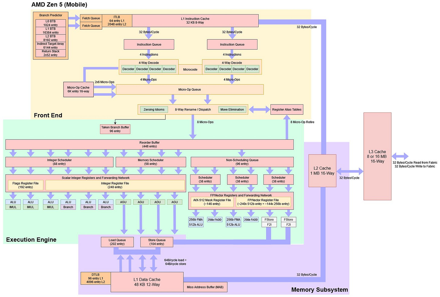
L1 <-> L2 data bus should be 64B/cycle in your last two figures.