AMD's 9800X3D: 2nd Generation V-Cache
Following the first generation of V-Cache found in the Zen 3 and Zen 4 X3D SKUs, AMD is now following up with the second generation of V-Cache which is a major change for AMD in terms of packaging.
For the first generation of V-Cache, AMD took a standard Zen 3/4 CCD, thinned it to about 20 microns then stuck a die full of SRAM on top supported with 2 structural dies alongside the SRAM dies. With the second generation of V-Cache, AMD has moved the SRAM die down beneath the compute CCD.
With this move, AMD has gotten rid of the two support silicon dies. In order to fit the SRAM die under the compute die, not only does the SRAM die have 64MB of SRAM but also it now has additional power distribution under the CPU cores. The GMI link from the CCD to the IO die is unchanged but now it has to route from the CCD down to the SRAM die into the C4 bumps.
Acknowledgement
We would like to thank AMD for sending us a 9800X3D and X870E board for testing.
The memory settings used for both the 9950X and the 9800X3D was 6000 CL32-39-39 unless specified.
Clock Behavior
With the first generation of V-Cache, the voltage tolerances of the stacked cache was reduced. For example, the maximum voltage tolerance of the 7800X3D was 1.2 volts with a nominal voltage of 1.1 volts. But with the second generation of V-Cache, AMD has improved the voltage tolerance to the point that both the 9800X3D and the 9700X both have a maximum voltage of 1.4 volts and a nominal voltage of 1.28-1.31 volts.
Much like the 9950X, the 9800X3D has very consistent clocking with delta of about 10 Mhz between cores. Compared to Clam’s 7950X3D V-Cache die which has about a 70MHz delta between cores, the 9800X3D clocks much more consistently.
However, it’s not quite all sunshine and roses. There is still a 300 MHz boost clock deficit between the 9700X and the 9800X3D. This means there is still an “optimization” problem where some games will prefer the higher boost clock of the 9700X compared to the larger L3 cache of the 9800X3D.
V-Cache Latency
Just like first generation V-Cache, second generation V-Cache adds the same 4 cycles of latency to a L3 hit.

But again, much like the first generation of V-Cache, this doesn’t show the full story.
Due to the higher clock speed along with not having the 4 cycle penalty, the 9950X has about a 14% decrease in absolute L3 latency. But again, in exchange for that penalty you do get a tripling in L3 capacity.
V-Cache Bandwidth
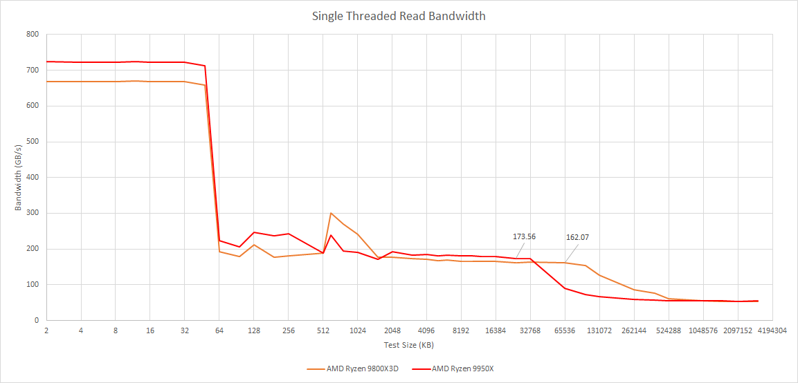
Much like the first generation of V-Cache, the stacked cache adds extra capacity to each L3 slice with the on-CCD interconnect staying untouched.
As we can see, the 9800X3D has nearly the same bandwidth as the 9950X with the only penalty being the clock speed difference.
Moving to the bandwidth of the CCD, and again we see very similar behavior between the 9950X and the 9800X3D where the difference lies in the clock speed deltas.
SPEC 2017 Performance
SPEC 2017 is an industry standard benchmark suite which is used by OEMs, CPU vendors, and others in the industry.
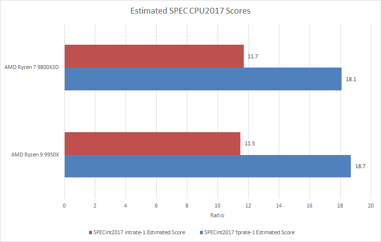
Despite the 500MHz clock deficit between the 9950X and the 9800X3D, the 9800X3D ends up ahead of the 9950X in the integer suite and in the floating point suite the 9800X3D largely makes up for the 500MHz clock deficit.
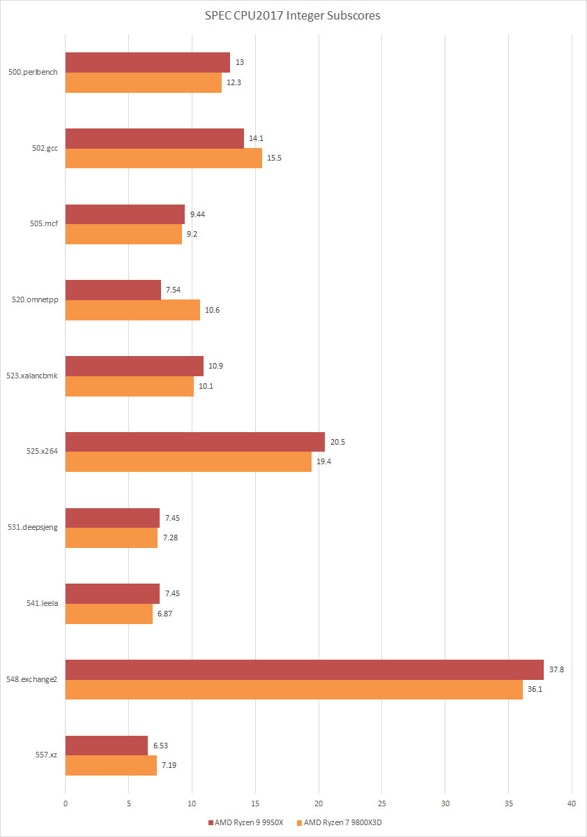
Looking a bit deeper, the integer subtest that gets the most benefit from V-Cache is the 520.omnetpp subtest which was most bottlenecked on the 9950X by being memory bound. V-Cache would alleviate this bottleneck so it’s unsurprising that the 9800X3D does well.
What is interesting is that 520.omnetpp is not the most memory bottlenecked test for Zen 5. While 502.gcc is more memory bound than 520.omnetpp and does see about a 10% performance increase on the 9800X3D, the most memory bound test is 523.xalancbmk which doesn’t really see a benefit from V-Cache.
Turning to the FP subtests and 503.bwaves is the big standout here. 503.bwaves is very compute bound so it’s no wonder that it prefers the higher clock speed of the 9950X over the V-Cache of the 9800X3D.
Unsurprising the two test that benefit the most from V-Cache, 549.fotonik3d and 554.roms, are also the two most memory bound tests. 549.fotonik3d and 554.roms see a 7.5% and a 15% performance uplift on the 9800X3D compared to the 9950X.
Conclusion
The biggest changes to second generation of V-Cache’s are physical. With the flipping of the cache and the CCD, this reduces the thermal resistance of the CPU quite a bit. While running Y-Cruncher while the CPU was running at 95C on a Noctua NH-D15, the 9800X3D was able to hold its base clock of 4.7GHz.
The second generation of V-Cache’s memory bandwidth and memory latency behavior is very similar to first generation V-Cache where the memory latency and bandwidth is near to identical to the non V-Cache SKUs other than the lower clocking of the V-Cache SKUs. In terms of the SPEC performance, the 9800X3D is ahead of the 9950X in the INT tests and just about makes up the clock speed difference in the FP tests.
In the end, AMD took what they learned with the first generation of V-Cache along with the MI300 series of accelerators and create the second generation of V-Cache which remediates the biggest weakness of the first generation of V-Cache which was the extra thermal resistance of the support silicon over the cores. This has allowed AMD to both stabilize the boost clock and increase the base clock.
I wonder what impact this will have on future AMD CPUs with regards to the packaging of their CPUs. Possibly in the future AMD will move all L3 cache into the base tile and just have the cores and L2 cache on top. Or mayhaps they will have more than 1 stacks on future CPUs.
If you like our articles and journalism, and you want to support us in our endeavors, then consider heading over to our Patreon or our PayPal if you want to toss a few bucks our way. If you would like to talk with the Chips and Cheese staff and the people behind the scenes, then consider joining our Discord.


Does anyone have details about how these new dies with a layer of v-cache embedded below cores are manufactured? Previously it required a separate die with the cache to be bonded to the cores die. Is it now part of a single chip? Do all zen 5 have this layer or is it a separate design?
> The GMI link from the CCD to the IO die is unchanged but now it has to route from the CCD down to the SRAM die into the C4 bumps.
Is there no additional latency due to this?