
Zen 5’s Leaked Slides

A YouTuber called Moore’s Law is Dead recently leaked a couple AMD slides about Zen 5. I typically find leaks uninteresting as they are impossible to verify and often don’t correspond to reality. One example is leakers expecting RDNA 3 to one-up Nvidia’s Ada architecture. AMD is fighting two larger competitors on two fronts and has not managed a decisive lead over Nvidia for more than a decade. AMD is expected to pull a miracle in the next generation, every generation (or two), and to everyone’s surprise it doesn’t happen.
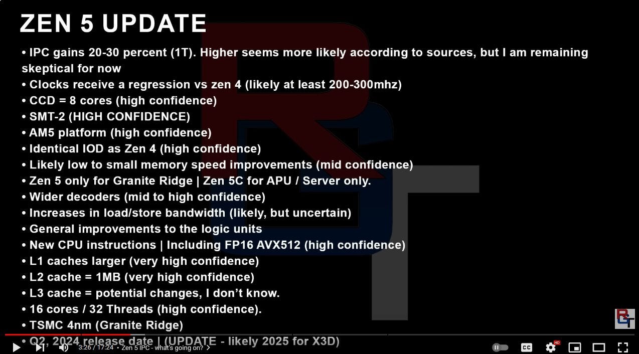
However, this leak is worth a mention because it includes a slide with architecture information. I don’t know whether the leaked slides are genuine, however building a coherent picture with a lot of details is far more difficult than fabricating a few performance numbers. With that in mind, let’s dig a bit into the slides point by point. Instead of trying to validate or disprove the rumors, I’ll try to provide context for each point so you can reach your own conclusions.
Branch Prediction
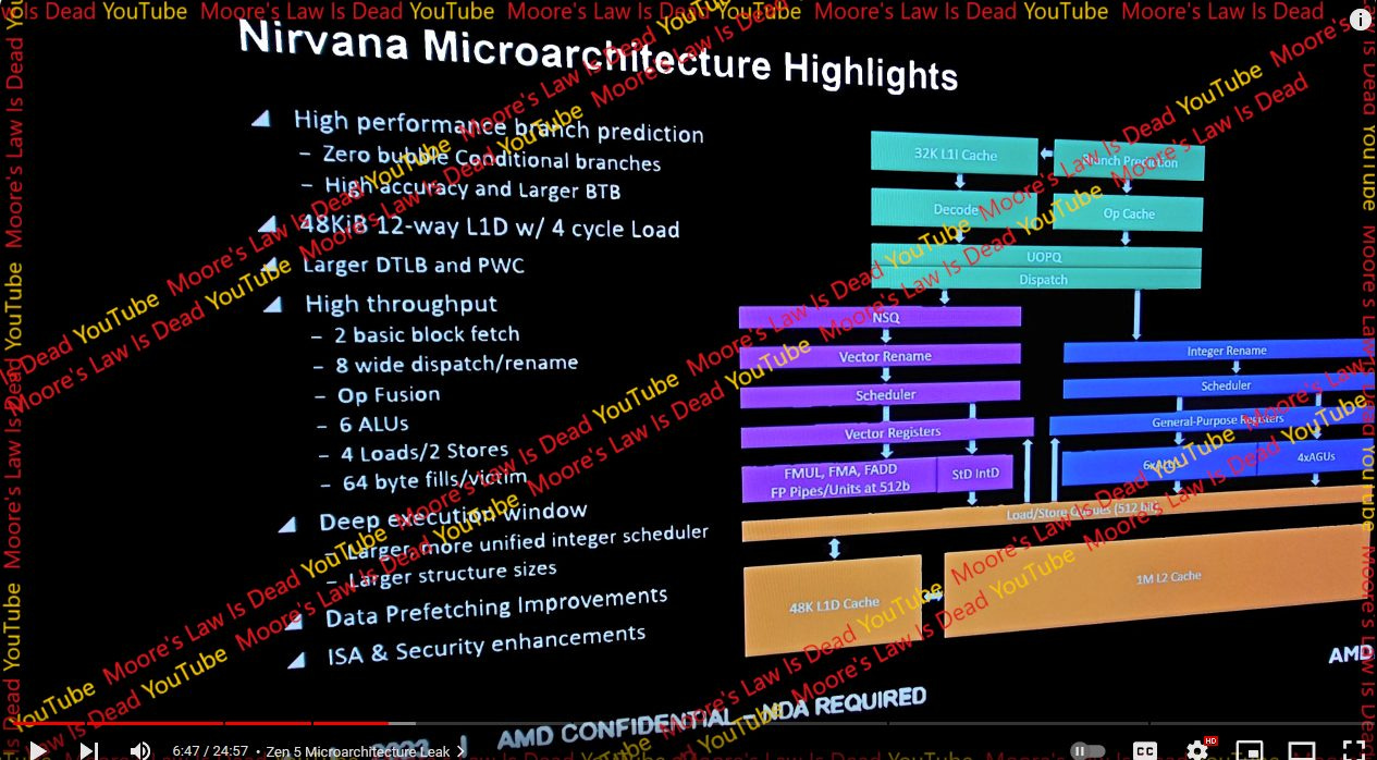
Branch predictors steer a CPU’s pipeline, making them vital to both power efficiency and performance. If a branch predictor takes too long to guess where a branch is going, it could hold up the rest of the CPU pipeline. If it guesses wrong, the core will waste time and power doing useless work. The leaked slide brings up three points under the branch predictor, namely zero bubble conditional branches, high accuracy, and a larger BTB.
Zero Bubble Conditional Branches
“Zero bubble” branching refers to handling a branch without delaying subsequent instructions in the pipeline. If later instructions were delayed, it would be analogous to a gas bubble in a pipe carrying liquid. Too many bubbles reduce how much liquid the pipe is delivering, and can be a problem if your production is constrained by how much liquid that pipe can deliver.

AMD could already do zero bubble branching since Zen 1, even though few branches could be tracked by the zero bubble predictor. Zen 3 expanded the zero bubble BTB (cache of branch targets) to cover 1024 branches, making zero bubble branches the typical case. Zen 4 carries this forward and expands zero bubble BTB capacity to 1536 branch targets. Therefore, zero bubble branching is nothing new. Zero bubble conditional branches aren’t new either. On all Zen generations, zero bubble branching can happen regardless of whether the branch is conditional or unconditional.

AMD isn’t alone either. Intel’s Haswell could track 128 branches and handle them with no bubbles. Intel thus made zero bubble branch handling a common case well before AMD did. Since Zen 3, AMD has been able handle more branches with zero bubble speed, but Intel is still very respectable in this area.
Therefore “zero bubble conditional branches” is not an exciting point. Existing CPUs from Intel, Arm, and AMD themselves can already handle conditional branches with zero bubbles. Maybe Zen 5 increases zero bubble predictor capacity, but the slide did not say so.
High Accuracy and Larger BTB
AMD has improved branch predictor accuracy with every generation. Zen 2, 3, and 4 could often achieve better branch prediction accuracy than their Intel competitors. Zen 5 certainly looks to maintain that lead. But saying a desktop CPU has “high accuracy” branch prediction is like saying an airliner has a pressurized cabin. You expect it to, and it’s news if it doesn’t. Even older, simpler branch predictors like the ones on AMD’s Phenom CPUs could correctly predict the vast majority of branches.
BTB stands for “branch target buffer”, which is a cache of branch targets. If a branch’s target is cached, the predictor can tell the CPU where to fetch instructions from next without waiting for the branch instruction to reach the core. That reduces frontend latency especially if the branch instruction has to be fetched from L2 or beyond. AMD has tweaked BTB size with every generation, but is a step behind Intel’s best.

Golden Cove’s L3 BTB has 50% more capacity than AMD’s last level L2 BTB, and frontend latency is a problem for Zen 4 in games. It’s likely a problem for Intel as well, and both companies will try to expand branch target caching capacity as transistor budget allows.
2 Basic Block Fetch
A basic block is a block of code with exactly one entry point and one exit point. A branch will terminate a basic block even if it’s conditional and not always taken. Existing AMD (and Intel) CPUs could already fetch across basic blocks because they could fetch across not-taken branches. The point on AMD’s slide could mean several things.

The simplest and most likely explanation is that Zen 5 can fetch across basic blocks just as any high performance CPU made in the last 20 years could. Usually the most boring interpretation of a marketing statement is the correct one.

Maybe Zen 5 can fetch across taken branches. Recent CPUs from Intel and Arm have done this. Rocket Lake could unroll small loops within its loop buffer, turning taken branches into not-taken ones from the fetch perspective. Arm’s Neoverse N2 and Cortex X2 can also sustain two taken branches per cycle by using a 64 entry nano-BTB. This capability can help improve frontend bandwidth for high IPC but branchy code. If an architectural feature has been around long enough to be implemented by multiple manufacturers, it has a better chance of showing up in a new core. Without being completely crazy, you could hope that Zen 5 can sustain more than one taken branch per cycle based on the leaked slide.
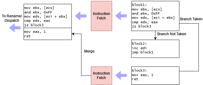
Finally, there’s the daydream category. AMD previously advertised zero-bubble branch handling when it became the common case with Zen 3. They didn’t mention zero-bubble branch handling with Zen 1 or Zen 2, even though both had limited ability to do zero-bubble branches. Maybe Zen 5 can fetch across basic blocks in the common case instead of using a loop buffer or micro-BTB as Intel and Arm did. That likely requires a dual-ported instruction cache or micro-op cache alongside a large BTB capable of delivering two branch targets per cycle. Zen 5 would also need circuitry to merge two fetch blocks into a buffer that downstream stages can consume. I think implementing such a strategy makes little sense. It’d only help in high IPC code bound by frontend throughput. Frontend latency due to instruction cache misses is a bigger issue.
Load/Store
Every CPU generation tends to see memory subsystem changes to reduce and hide latency.
Increased L1D Capacity
The leaked slide says Zen 5 has a 48 KB 12-way set associative L1 data cache, giving it increased capacity and associativity compared to Zen 4’s 32 KB, 8-way L1D. Impressively, the slide claims latency stays at 4 cycles. Intel did the same with their L1 data cache in Sunny Cove, but increased latency from 4 to 5 cycles.
Zen 5’s larger L1D will enjoy increased hitrate. Higher capacity helps reduce cases where a code sequence’s working set exceeds cache capacity. Higher associativity helps prevent conflict misses where cache capacity is sufficient but too many “hot” addresses clash into the same set.
I’m surprised AMD was able to pull this off because 12-way associativity means a cache access involves 12 tag comparisons. Zen uses a micro-tagging scheme where partial tags are compared to predict which cache way (if any) will have a hit, but comparing 12 micro-tags is still no joke. The slide also says Zen 5 can do 4 loads per cycle. That would require 48 tag comparisons.
Larger DTLB
All modern CPUs use virtual memory. Program memory addresses don’t directly address locations on DRAM chips. Instead, the operating system sets up a map of virtual addresses to physical addresses (page tables) for each process. A misbehaving process therefore won’t run over everything else and force you to reboot the computer because it has limited access to system memory.
However, virtual memory addresses have to be translated to physical addresses. If the CPU checked the page tables for each memory access, latency would skyrocket as each program memory access turns into several dependent ones. Therefore, CPUs use TLBs (translation lookaside buffers) to cache frequently used translations.

Zen 4 already enjoyed a first level data TLB size increase from 64 to 72 entries. Because of their small size, the first level TLB is fully associative. That eliminates conflict misses, but means any TLB entry could contain the desired translation. Four data cache accesses per cycle could require more than 72 * 4 = 288 TLB tag comparisons every cycle. I’m not sure how Zen 5 would increase the DTLB size without impacting latency unless AMD dropped the fully associative scheme.
I could see Zen 5 using a 16-way set associative DTLB with 128 entries or something along those lines. Checking it would be easier than with a 64 entry fully associative TLB, and the larger capacity could be enough to minimize conflict misses. Alternatively, Zen 5 could leave the first level DTLB untouched and increase L2 DTLB capacity. Zen 4 already brought L2 DTLB size up to 3072 entries compared to 2048 entries in Zen 3. Increasing L2 DTLB size would help programs with hot memory footprints in the multi-megabyte range.
Larger PWC (Page Walk Cache)
An address translation doesn’t have to be an all-or-nothing scenario where you either hit in the TLBs or do a full page walk. CPUs can cache upper level paging structures to reduce page walk latency when the TLBs can’t contain a program’s working set.

That lets the page walker start at a lower level, letting a page walk complete with fewer memory accesses. Each page walk cache entry covers a larger region in memory than a TLB entry, making it ideal for handling programs with a larger memory footprint than the L2 DTLB can reasonably cover. For example, a cached page directory pointer table entry would cover 1 GB of address space.
I’ve seen a lot of Reddit comments where people said they didn’t understand my articles, so I can explain this in plain English with a real life analogy. Imagine you need to walk your dog down four blocks. You want it done faster. An obvious answer is to build a trebuchet that can throw you and your dog down two blocks. Then, you can start the walk closer to your destination. Because different destinations exist, you build 64 trebuchets facing in different directions. Now, you have a real life walk cache.
If you build more powerful trebuchets, you can start your walk closer to the destination. But less powerful ones can throw you places that are a short walk away to many destinations. You can build a lot of more powerful trebuchets but that would consume more area (and trees). CPU architects have to make the same tradeoff.
Since Zen 1, AMD has used a 64 entry page directory cache (PDC) that holds page directory pointer table and page map level 4 entries. L2 TLB entries can cache page directory entries. Perhaps Zen 5 finally increases PDC size. Or maybe, AMD gave the load/store unit a stronger preference for caching page directory entries in the L2 TLB compared to direct translations.
High Throughput
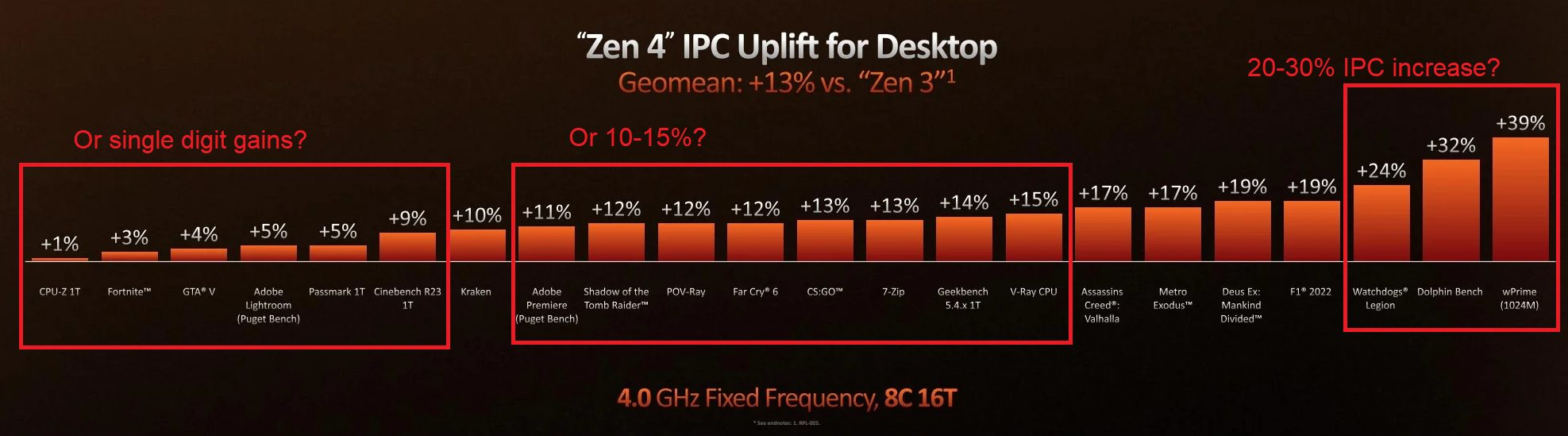
Zen generations have seen modest improvements in core throughput, because core throughput is typically not a limiting factor. Zen 1 and 2 could sustain 5 instructions per cycle, while Zen 3 and 4 could sustain 6 per cycle. AMD made double digit IPC gains every generation thanks to large improvements to instruction and data side memory access performance.

But a small minority of high IPC applications might benefit.
8-Wide Dispatch/Rename
Every Zen generation had at least an 8-wide frontend and 8-wide retire. However, the dispatch/rename stage was only 6 micro-ops wide. If Zen 5 makes rename/dispatch 8-wide, it would be able to sustain 8 micro-ops per cycle.

This change will benefit a small minority of high IPC applications capped by core width. Lower IPC applications like games will see little benefit from this change because they’re primarily bound by cache and memory latency.
Op Fusion
CPUs can achieve higher throughput and make better use of internal buffers by fusing adjacent instructions into single micro-ops. Branch fusion is the most common example. Conditional branching on x86 involves using an instruction that sets flags, and then a branch that jumps (or not) depending on flags. Intel and AMD have been fusing such ALU + conditional branch pairs for many generations. Arm’s recent cores do the same for equivalent ARM64 sequences.
Zen 3 improved AMD’s fusion capabilities by allowing simple ALU instructions like ADD, AND, and XOR to be fused with a subsequent branch as well as CMP and TEST. Therefore one micro-op on Zen 3 can perform a math operation, check the result for a condition and branch on it, and write the result back to a register. Zen 4 added NOP fusion and XOR+DIV/CDQ+IDIV fusion. The latter handles common use patterns for x86’s division instructions.
Maybe Zen 5 expanded fusion cases, but the slide did not say so. For all we know, the slide could be reiterating the features already present on Zen 4. Prior Zen generations already covered the most common fusion cases (branches). Zen 4’s improvements chase diminishing returns. NOPs are used to align code and should account for a very small percentage of executed instruction. Division is known to be very expensive and avoided by most compilers. If Zen 5 adds fusion cases, it’ll probably pursue further diminishing returns.
Larger, More Unified Scheduler
Schedulers sit at the heart of an out-of-order CPU and let them achieve high instruction level parallelism. Every cycle, a scheduler has to watch what registers are written to and see if pending instructions need those inputs. It also has to select instructions that have all their inputs ready and send them to execution units. Failing to accomplish all that in a single cycle incurs a ~10% IPC penalty, so large, fast schedulers are very difficult to design. Small schedulers are easy to make fast but can fill quickly and prevent the core from hiding latency. Fortunately, engineers have a lot of scheduler layout options available.
In a distributed scheduler, each execution port gets its own private scheduler. That simplifies scheduler design because each scheduler only has to select one instruction for execution each cycle, and only needs enough entries to hold the fraction of pending instructions that are expected to be waiting for that port. However, tuning is difficult because one scheduler can fill and block the renamer even if scheduler entries are available elsewhere.

A unified scheduler avoids that problem by having one scheduler serve multiple ports. Each scheduler entry can hold an instruction destined for any port, so a sudden spike in demand for one execution port can be better tolerated. However, a unified scheduler has to select enough instructions per cycle to feed all the execution ports it’s attached to. There’s no free lunch.

AMD, Intel, and Arm’s recent CPUs use a hybrid of the two approaches. Zen 5’s scheduler is both larger and more unified, meaning it has more total entries and can use some of them more efficiently.

From a look at a couple of gaming workloads, integer scheduler 0 fills a bit more often than the others. Cinebench 2024 sees similar behavior on the integer side.

Scheduler 0 feeds an AGU pipe and an ALU/branch pipe. AMD could chose to make this scheduler bigger or unify it with another scheduler. They could combine both approaches as well. However, scope for improvement may be limited. Integer scheduler related dispatch stalls account for single digit percentages, indicating Zen 4’s distributed scheduler is already well tuned.
6 ALUs, 4 loads, 2 stores
The slide says Zen 5 has 6 ALUs, and the ability to do 4 loads/2stores per cycle. ALUs, or arithmetic logic units, are execution units capable of handling the most common integer instructions like adds and bitwise operations. All prior Zen generations had four ALUs, so Zen 5 would increase per-cycle scalar integer throughput by 50%.
This change will have minimal effect. I put this section right after the scheduler one because schedulers will fill if the execution units can’t keep up with incoming operations. Schedulers can fill for reasons other than lack of execution ports as well. For example, a sequence of latency-bound instructions will also fill the schedulers. Scheduler-bound dispatch stalls are therefore an upper bound on how often the core is execution unit bound. From above, it doesn’t happen often.
Increased load/store throughput might help specific scenarios like memory copies, where the core can sustain 2 loads and 2 stores per cycle but how much this will effect general cases, I don’t know.
ALUs and AGUs themselves are tiny, but feeding them is more difficult. Each new execution port needs inputs from the register file, and increasing register file port count will increase area. More execution ports mean schedulers will have to pick more instructions per cycle, requiring more power and area as well.
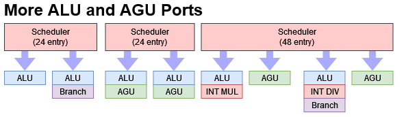
If I were AMD and had to implement 6 ALUs and 4 AGUs, I would do so with the absolute minimum of extra ports. AGU ports can do double duty as ALU ports because AGUs already have to do simple math on register inputs anyway. The branch port can also be upgraded to an ALU, again reusing existing register file ports.
Increasing execution unit throughput will result in minimal gains, but minimal gains can be worthwhile if they are achieved at low cost. I suspect AMD is going after that route.
Larger Structure Sizes
An out-of-order CPU has structures to track instruction state until their results can be made final. Structure sizes tend to increase with every CPU generation. The leaked slide suggests Zen 5 will do so too, but did not go into specifics.

In Cinebench 2024 and the tested games, Zen 4’s reorder buffer is responsible for most stalls. The reorder buffer tracks all instructions in the backend until they are committed in-order. It’s a cap on how far ahead the CPU can move ahead of a stalled instruction. Filling the reorder buffer isn’t a bad thing because it means other queues for specific instruction categories are large enough to not become limitations themselves.

AMD has increased reorder buffer capacity with every CPU generation. Zen 5 will almost certainly see an increase as well, but we don’t know to what extent. Along with a reorder buffer capacity increase, AMD will have to augment other structures to prevent them from filling before the ROB does. The store queue could already use more entries and is a prime candidate for optimization. However, increasing store buffer size will be difficult because it has to hold pending store data. For Zen 4, that’s up to 32 bytes per store.
64 Byte Fills/Victim
This line on the slide talks about caching. “Fills” refers to cache fills, and “victim” refers to lines kicked out of a cache to make room for data being filled in. I’m confused because every CPU in recent history uses 64 byte cache lines, which means caches manage data at 64 byte granularity. Thus, data is evicted 64 bytes at a time, and brought in 64 bytes at a time. It’s not a point worth mentioning.
Data Prefetching Improvements
Better caching and higher reordering capacity help attack the memory latency problem by reducing latency and allowing execution to proceed past a latency-bound instruction, respectively. Prefetching counters memory latency by trying to get data that the program will need before an instruction asks for it. Again, the slide didn’t go into specifics, so I’ll provide context on what Zen 4 does.

In Zen 4, AMD has prefetchers at the L1 and L2 level. Zen 5 may keep the same prefetch methods but allow them to prefetch further, taking advantage of any bandwidth increases offered by more mature DDR5 implementations. AMD may also tune the prefetchers to ensure demand requests get priority when there’s high bandwidth demand, such as during multi-core workloads.
Better AVX-512
Zen 4 featured AMD’s first AVX-512 implementation. Unlike AMD’s first SSE and AVX implementations, Zen 4 did not break instructions that operated on 512-bit vectors into two micro-ops. It had full width 512-bit vector registers, and kept AVX-512 math instructions as one micro-op until they were executed 256 bits at a time.

Keeping the same FP execution throughput as Zen 2 and Zen 3 helped AMD get the most important AVX-512 benefits (more efficient use of backend resources) without a massive increase in die area and power.
The slide says “FP Pipes/Units at 512b”. The most optimistic interpretation is that Zen 5 has 2×512-bit FP vector execution. Even on TSMC’s newer 4 nm process, I feel that’ll cost too much area and power when most consumer applications don’t use 512-bit vectors. Perhaps AMD will create Zen 5 variants with different FP configurations as Intel has done, with client SKUs spending less area and power on vector FP throughput.
512-bit stores are handled less efficiently on Zen 4 because the store queue can only hold 256-bit pending store data with each entry. At Hot Chips 2023, AMD stated that the area overhead of buffering 512-bit store data was not acceptable. The leaked Zen 5 slide says “Load/Store Queues (512 bit)”, so AMD may have changed their stance.
Applications that heavily leverage 512-bit vectors should see more performance uplift on Zen 5 thanks to these changes.
Final Words
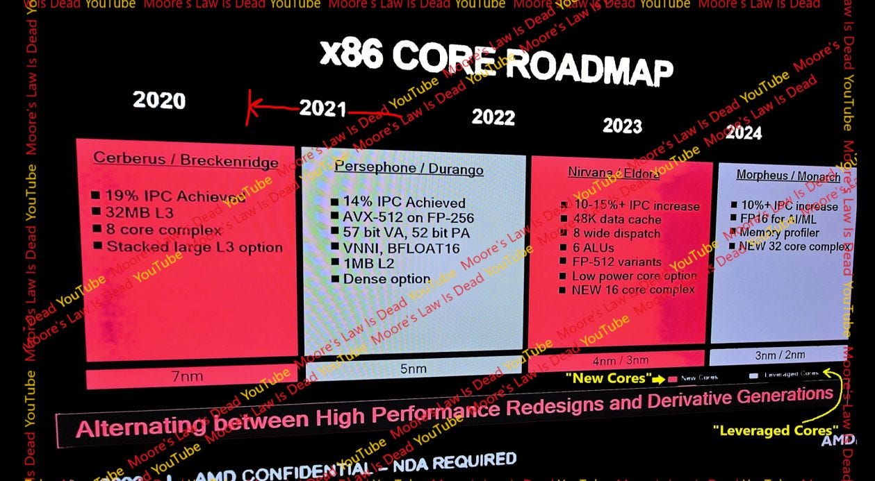
From the leaked slides, AMD is pursuing diminishing returns after getting most of the low hanging fruit with prior Zen generations. Zen 2 greatly improved branch prediction accuracy, vector throughput, and cache capacity compared to Zen 1. Zen 3’s improved BTB setup mitigated Zen 2’s frontend latency problem, and a reorganized scheduler avoids situations where Zen 2’s AGU scheduler fills up. Zen 4 brought a bigger micro-op cache, improved L2 capacity, a substantially increased out-of-order execution window, and AVX-512 support. Zen 5 appears to be going after more limited gains by increasing core throughput and providing a stronger AVX-512 implementation.

That said I would caution against looking too far into the current leaks. Specific details are rare, leaving plenty of wiggle room. Assuming Zen 5 is set in stone at this point is also perilous. Core behavior can be tuned via microcode updates. A core can be configurable as well, giving AMD the potential to make large changes even when the architecture is “complete”. We’ve seen AMD roll out Zen 2 variants with different FPU configurations. In the same video, MLiD showed another slide that suggests different FP-512 variants exist as well.
Any performance numbers should be taken with a giant grain of salt too. It’s better to assume they are all guesses at this point. Even if a leaker has a “source”, estimating performance is inherently difficult because different applications will behave differently. An engineer might see a 30% IPC instruction uplift in simulation with a specific instruction trace, but that doesn’t mean other applications will enjoy the same improvement.
That could be mentioned to a leaker, who doesn’t understand that the trace may not be representative of most applications.
Finally, engineers at Intel, AMD, Arm, and other companies put a lot of hard work into their products. It’s only fair to let them get their say when a product is released. If the engineers release a solid product that delivers a typical 10-20% generation on generation gain but everyone’s perception is set based on fabricated or misinterpreted early performance numbers, I think that’s disrespectful to the engineers. It’s also nonsensical when Intel delivered lower generation on generation gains at the top of their game in the early 2010s.
AMD is prone to this because they’re an underdog that people expect to one-up its bigger competitors, so fanciful rumors get a lot of attention. Whenever Zen 5 comes out, I would encourage everyone to look at its performance with respect to how Intel and other CPU manufacturers are progressing, and not based on rumors.
If you like our articles and journalism, and you want to support us in our endeavors, then consider heading over to our Patreon or our PayPal if you want to toss a few bucks our way. If you would like to talk with the Chips and Cheese staff and the people behind the scenes, then consider joining our Discord.