
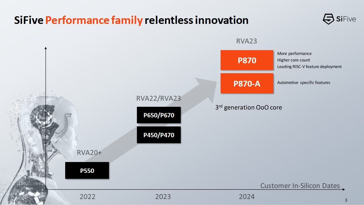
Hot Chips 2023: SiFive’s P870 Takes RISC-V Further

RISC-V is an open instruction set architecture, which means that anyone can create a core that understands RISC-V instructions without worrying about patents and licenses. SiFive is an important player in the RISC-V scene, and creates custom RISC-V cores that other companies can license. SiFive presented their P870 core at Hot Chips 2023. It aims for higher performance than prior SiFive designs, and should sit in the same ballpark as ARM’s Cortex X2 or AMD’s Zen 4c.
High Level
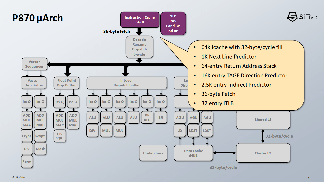
SiFive’s P870 is a six-wide core featuring out-of-order execution. Reordering capacity is quite substantial, thanks to a large reorder buffer and strong instruction fusion capabilities. The core has a pile of modern features like a decoupled branch predictor, non-scheduling queues (dispatch queues); and notable for a RISC-V design, vector execution capability.
From SiFive’s pipeline diagram, P870 looks to have an eight cycle misprediction penalty, which is quite short compared to contemporary CPUs from ARM, AMD, and Intel. If a mispredict is discovered at the Ex stage and the pipeline can restart from the instruction cache lookup stage, mispredict penalty would be just seven cycles.

P870 therefore has a very short pipeline, despite not using a micro-op cache. During the Q&A session, Brad Burgess stated that clock speeds would be competitive and go well into the 3 GHz range. If so, SiFive has done a pretty impressive job of hitting decent clock speeds with a shorter pipeline than its competitors.
Branch Predictor
The P870’s pipeline starts at the branch predictor, which tells the frontend where to go. Direction prediction is provided by an eight-table TAGE predictor with 16K table entries. A TAGE (TAgged GEometric) predictor works by picking between a set of sub-predictors that use different history lengths. In this case, SiFive is likely using eight sub-predictors, with 16K total entries across those tables.
P870’s branch predictor generates a fetch target over several pipeline stages. First, a fast zero-bubble predictor generates a target address, which is passed to the instruction cache to begin the fetch process. After that, the TAGE predictor completes its prediction and can override the zero-bubble predictor for what looks like a 2 cycle penalty. Finally, indirect branch prediction takes place in the next cycle, which overlaps with instruction decode. An indirect prediction would therefore incur a three cycle penalty. For comparison, AMD’s Zen 4 has a similar three cycle penalty for indirect predictions or L2 BTB overrides.
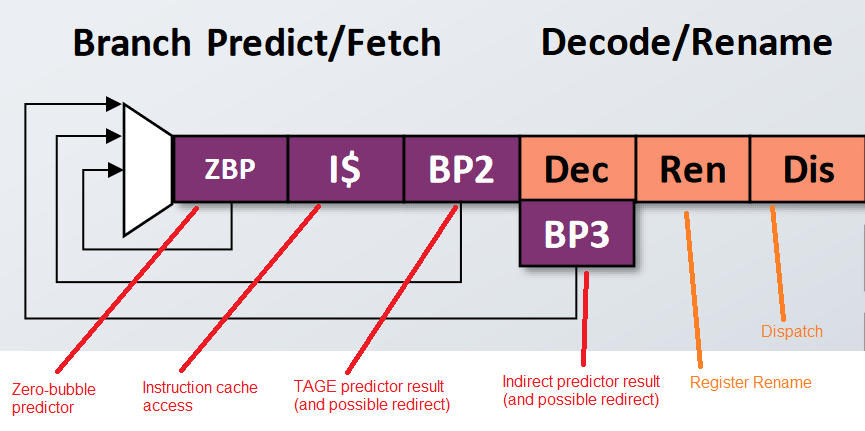
SiFive gave the zero-bubble predictor 1024 entries, letting P870 match AMD’s Zen 3 in terms of zero-bubble branch tracking capacity. Other branch prediction resources are ample as well. A 64 entry return address stack is extremely large and borderline overkill. AMD’s Zen line only has 32 entry return stacks and can predict returns with very high accuracy already. The indirect predictor’s 2.5K entry capacity is quite respectable too. Zen 4 has a 3072-entry indirect predictor, while Zen 3 has a 1536 entries. P870’s indirect predictor therefore slots in right between those two Zen generations.
Instruction Fetch
Once the branch predictor has generated a fetch address, P870’s frontend can fetch 36 bytes per cycle from its 64 KB instruction cache. We’ve been assured that 36 bytes per cycle is not a typo, and that P870 can fetch 9 RISC-V instructions worth of bytes every cycle to feed its 6-wide decoder. A 32 entry iTLB helps cache virtual to physical address translations on the instruction side. It’s a bit small compared to the 64 entry iTLB on AMD’s Zen 4, but SiFive is confident that it’s good enough for the workloads they’re targeting.
P870’s decoders handle a lot of instruction fusion cases, though SiFive didn’t go into specifics. We’ve seen x86 cores fuse compares and conditional branches, or NOPs with adjacent instructions. SiFive hints that P870 is capable of much more.
Some people may argue “Well, why doesn’t RISC-V have more complex memory addressing modes for example. The philosophy, which I think is an interesting one, is to take those instructions that you build that up with and fuse them, as opposed to just eating up opcode space”
Brad Burgess at Hot Chips 2023
Instruction fusion is quite intuitive to understand. For example, a German person may read an English phrase with five tokens, like “financial market stabilization act” and fuse it into a single micro-op (finanzmarktstabilisierungsgesetz) for more efficient use of brain resources. We’ll have to wait and see how well this strategy works for RISC-V, because instruction fusion requires the fused instructions to be adjacent. Compilers will have to arrange instructions to make this possible.
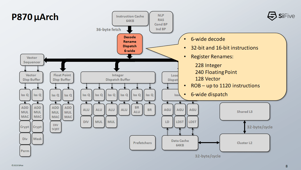
Once instructions have been decoded, any register references are appropriately renamed to refer to the corresponding physical register file entries. Other backend resources are allocated as needed, and the instruction can be tracked by the out-of-order execution engine.
Execution Engine
P870 has a large backend, with resources roughly comparable to that of ARM’s Cortex X series or AMD’s Zen 4. Reorder buffer and register file capacity are similar across all three cores, though P870’s load and store queues are a bit light.

SiFive has chosen an execution port layout that has some parallels to ARM’s strategy with Cortex X2. They’re spamming small distributed schedulers, leading to tons of execution ports. Distributed schedulers can be hard to tune, because any one scheduling queue filling up could lead to a stall. To counter this, SiFive is using a similar strategy to Apple’s Firestorm. Every execution cluster has a non-scheduling queue to prevent renamer stalls if scheduling queues fill.

On the execution unit front, P870 features a total of six ports. Port count thus matches Cortex X2, but every port gets a dedicated scheduling queue. And while Cortex X2 dedicated two ports to handling branches, P870 makes one of the branch ports also capable of handling general ALU operations.
Floating Point Execution
Floating point execution resources are sparser than on the integer side. P870 has two FP pipes, each capable of handling the most common operations. SiFive is keen to emphasize its excellent 2 cycle latency for FP add and multiply.

Unlike most other CPUs today, SiFive’s presentation suggests P870 has separate FP and vector register files. They have different numbers of renamed registers available, and one is not a multiple of another (making a fusion case unlikely). If so, the floating point and vector register files individually can have lower port counts. Feeding two multiply-add units requires six inputs, and lower port count should allow more area efficient register files.
Vector Execution
P870 supports vector execution with a pair of 128-bit wide pipes. This is a weak point in P870’s architecture, but it’s still a solid step forward in the RISC-V world. Other RISC-V chips like Ventana’s Veyron V1 only have scalar FP execution and no vector execution capability at all. A pair of 128-bit pipes roughly matches what ARM has on their Neoverse N1 and N2, and can provide passable vector performance.

P870 features a unique coping mechanism aimed at RISC-V’s LMUL feature, caled the vector sequencer. An insane programmer can set LMUL to a value higher than 1, making vector instructions address contiguous blocks of registers. Normally, weird complex things are handled by the decoder splitting the instruction into multiple micro-ops. But doing so would consume a lot of decoder and renamer bandwidth if LMUL is not 1.

Therefore, SiFive splits vector instructions further down the pipeline if LMUL > 1. Doing so means an instruction with LMUL = 2 would only consume one decode slot. After the sequencer, it would consume multiple scheduler slots and have its micro-ops issued over as many cycles as necessary.

A closer look at P870’s vector pipeline suggests the sequencer can break up a vector operation in as little as one cycle. The vector unit has its own register rename stage placed after the vector sequencer, so physical registers are allocated after a vector operation is split up. As with all new architectural features, we’ll have to wait and see how useful RISC-V’s LMUL will be.
Cache and Memory Access
P870 has three pipes for address generation. Two pipes can handle loads or stores, while a third pipe only takes loads. This AGU setup is similar to what we see on Cortex X2, A710, and Zen 4. Data cache access takes four cycles. Curiously, address generation, tag lookups, and data cache access take place over three cycles. P870 spends an extra pipeline stage (Drv) just to move data around. I wonder if a future design could see 3 cycle load-to-use latency. It should be completely doable. After all, AMD’s Athlon line achieved 3 cycle latency to 64 KB L1Ds on ancient process nodes, while running at similar frequencies.

Address translation is handled by a 64 entry DTLB, backed by a 1024 entry L2 TLB. The L2 TLB is a bit small these days, but ARM has a similar L2 TLB size on their Cortex A710.

L1D misses are handled by a shared, non-inclusive L2 cache. The L2 cache is banked to handle access from multiple cores, and has a latency of 16 cycles. Intel’s E-Cores are similarly arranged in quad core clusters with a shared L2, and see 20 cycles of L2 latency. SiFive lets customers configure L2 size, but they gave a 4 MB L2 configuration as an example. To handle coherency, the L2 complex maintains snoop filters to track core-private cache contents, in a scheme that sounds similar to what Cortex A72 used.
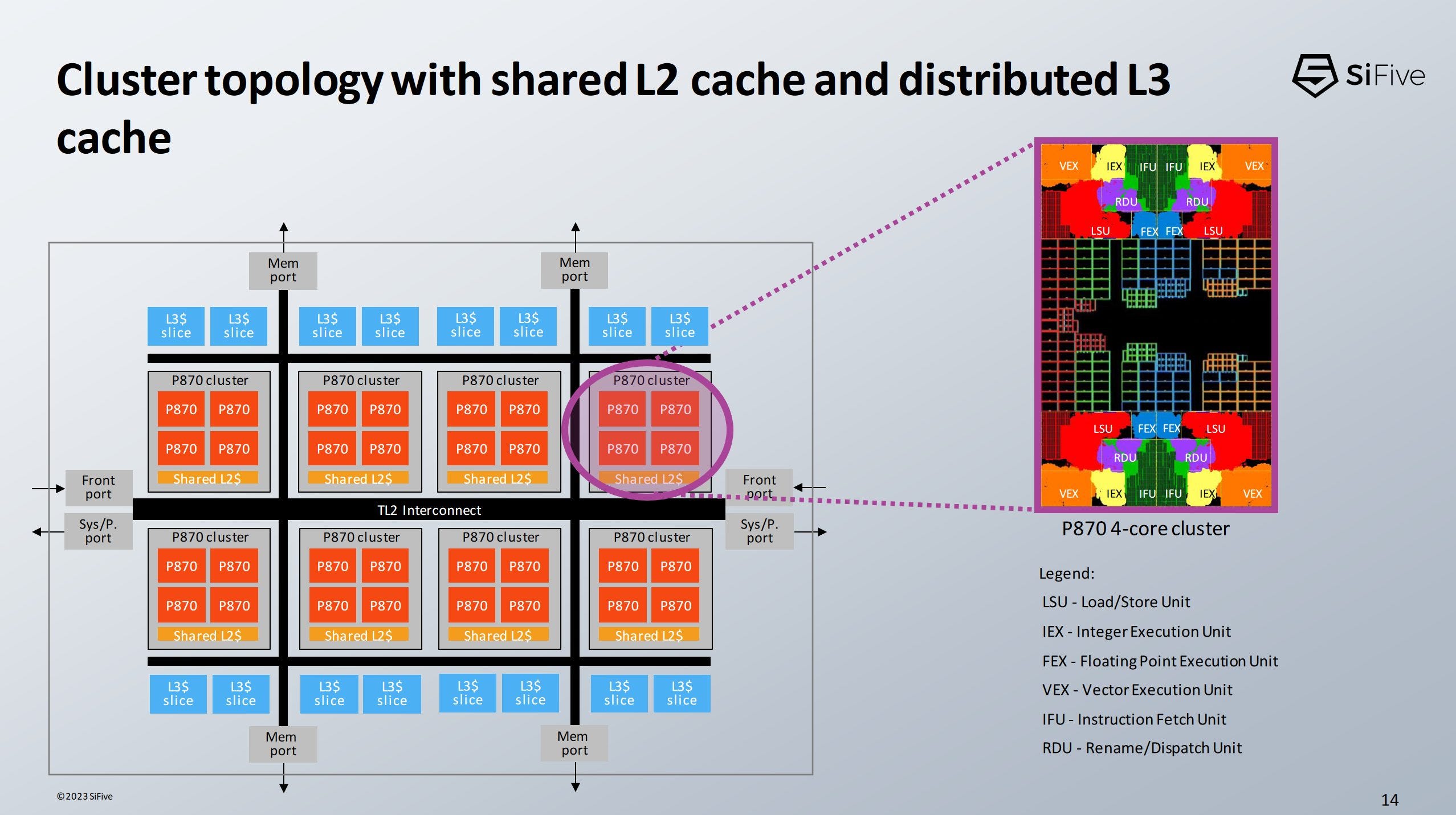
P870’s L3 cache is shared across clusters. L3 capacity and latency are implementation dependent, but SiFive used a 16 MB L3 configuration for their performance estimates.
Reliability Features
Just about every modern CPU protects various caches and other structures to improve reliability. SiFive’s P870-A is an automotive variant of the P870 core that pays particular attention to error detection and correction. After all, no one wants a system to crash and cause a car crash.

Besides the standard set of ECC and parity protections for caches and register files, SiFive has implemented high reliability cache controllers and interconnects. I’m not sure what SiFive specifically did to make those components more robust, but other CPUs often have parity or ECC protection on the various queues and transmit links in their interconnects. For example, Zen 4’s Scalable Data Port (interface to Infinity Fabric) is parity protected, and queue in front of the UMC (memory controller) is ECC protected.

Finally, SiFive can run pairs of P870 cores in lockstep to further improve reliability, a bit like how aircraft and spacecraft run redundant computations across multiple computers. A random bit flip is unlikely to impact multiple cores in the same way, so this approach dramatically increases reliability by basically duplicating all core structures, at the cost of less compute throughput. This kind of lockstep operation is possible because each core starts with a well defined state after reset, and operation after that is deterministic.
Final Words
ARM had a slow start on its way to move beyond microcontrollers and enter the high performance market. ARM Ltd made the Cortex A9, their first out-of-order core, in 2007. Throughout the 2010s, they gradually made bigger, higher power, and higher performance cores. Pushing performance boundaries isn’t easy, but today, ARM’s cores can be a viable alternative to Intel and AMD’s offerings in the server market.

RISC-V started much later, but has seen faster growth. Berkerly’s BOOM core had grown into a sizeable out-of-order design by 2016. Now, SiFive’s P870 looks a lot like ARM’s Cortex X series in terms of reordering capacity, core width, and execution units. It might not be a match for ARM’s best, since the load/store queues look a bit small and vector execution throughput is a bit weak. But from looking at P870, SiFive’s ambitions are clear. They want a chunk of ARM’s pie.

SiFive’s biggest challenge is going to be the software ecosystem. RISC-V’s vector extensions are still in their infancy. Not a lot of people are going to be familiar with RISC-V. Compilers will have to be tuned to ensure instruction fusion cases happen as often as possible. ARM has had a rough time getting their footing in the software world, and RISC-V will have to go through the same arduous process.
We’d like to thank SiFive for an excellent presentation at Hot Chips 2023, and hope to see P870 implemented in chips sometime soon.
If you like our articles and journalism, and you want to support us in our endeavors, then consider heading over to our Patreon or our PayPal if you want to toss a few bucks our way. If you would like to talk with the Chips and Cheese staff and the people behind the scenes, then consider joining our Discord.