
Hot Chips 2023: Ventana’s Unconventional Veyron V1

The RISC-V scene has been heating up. SiFive’s designs have moved into higher power and performance envelopes. Alibaba’s T-HEAD division has been creating RISC-V chips in a bid to develop a viable line of indigenous server CPUs. Now, Ventana is joining the party with their Veyron V1 core. In this article, I’ll analyze Veyron V1’s design, and pay particularly close attention to some of Veyron V1’s unusual features.
High Level
Veyron V1 is an eight-wide out-of-order core with a 15 cycle mispredict pipeline and substantial scheduler capacity. Like ARM and SiFive’s designs, V1 aims for modest clock targets in exchange for low area and power, letting Ventana scale to very high core counts. Ventana targets 3.6 GHz, but Veyron V1 can clock lower to reduce power consumption. At 2.4 GHz, the core pulls less than 0.9 W of power.

Pipeline
Veyron V1’s pipeline might seem a bit long at first glance. For comparison, AMD’s Zen 4 has a minimum mispredict penalty of 11 cycles, and ARM’s Neoverse N2 has a pipeline depth of 10 cycles. I assume ARM is also referring to the minimum mispredict penalty in their prior Hot Chips presentation, because that’s usually what people mean when they talk about pipeline length.
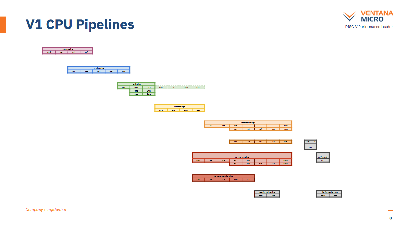
Ventana states that their newer V2 architecture improves mispredict penalty, and their slide backs this up. A mispredict detected at the first integer execution stage (IX1) will trigger a pipeline restart at the RPS (Restart Pipe Start) stage, which will overlap with IX1. That’s two stages away from the stage labeled PNI in the predict pipe. PNI almost definitely stands for Predict Next IP, which is where the next instruction pointer would be generated.
A mispredict can be detected either by comparing the true branch direction with the predicted one, or by comparing the targets. Feeding either the real target address or correct direction back into the branch predictor should let the pipeline restart right after PNI, cutting mispredict penalty by two cycles (down to 13 cycles).
Branch Predictor: Single-Level BTB
Like other modern CPUs, Veyron V1 has a decoupled branch predictor that can run ahead of fetch and decode, acting as a very accurate instruction prefetcher. To get the most out of this technique, the predictor has to be both accurate and be able to track a lot of branch targets. Large branch target caches (BTBs) are vital to letting the predictor follow taken branches without waiting for the branch instruction’s bytes to show up at the core, which would incur cache latency.
But big and fast caches are hard to make regardless of whether you’re caching branch targets or data. Therefore, recent CPUs have opted for multi-level BTBs. Typically, a fast first-level BTB allows back-to-back taken branches, while slower BTB levels help maintain decent performance for larger branch footprints.
Despite the usual tradeoffs between speed, capacity, and complexity, Ventana has picked all of the above. V1 has a single massive BTB level with 12K entries, and a “single cycle next lookup predictor”. With Berkerly’s BOOM, the “next line predictor” includes a BTB lookup, so I take Ventana’s slide to mean the 12K entry BTB can do back to back taken branches. This is quite an accomplishment, and lets V1 handle very large branch footprints with minimal throughput loss around taken branches. For perspective, Intel’s Golden Cove has a 12K entry last level BTB with three cycle latency.

If the BTB doesn’t provide the right target, V1 can do a “three-cycle redirect on mispredict”. This likely means the branch address calculator is three cycles away from instruction fetch, or basically in the first decode stage because V1’s instruction cache has two cycle latency. I expect such branch address calculator overrides to be relatively rare, thanks to the large 12K entry BTB.
Frontend: 512 KB L1/L2 Instruction Cache
Ventana has cut levels out of the instruction caching hierarchy too. Veyron V1 has a large 512 KB instruction cache that fills the role of both the L1 and L2 caches in other designs. A small loop buffer sits in front of the instruction cache, but this is primarily a power optimization for tight loops. V1 is expected to feed its pipeline from the 512 KB L1/L2 cache most of the time.
Veyron V1’s frontend design will work best for large instruction footprints that spill out of the 32 or 64 KB instruction caches we’re used to seeing. In such cases, other CPUs will waste power and time checking L1i on the way to L2, and swapping instruction bytes between the two cache levels.
But V1’s design forces a split L2 arrangement, sacrificing the caching capacity flexibility we see on other CPUs. A unified 1 MB L2 could use nearly all of its capacity to hold data if a little bit of code is looping over a lot of data. Or, more capacity could be dedicated to instruction caching if an application’s data footprint is small, but the code footprint is not.
If Ventana tried to use a unified L2 cache, instruction fetch traffic could cause contention with data-side L2 accesses. A CPU’s frontend is a heavy consumer of cache bandwidth because every instruction has to be fetched by a frontend memory access, but not every instruction will ask for a data-side memory access. Furthermore, less than perfect branch prediction could lead to more than one frontend memory access for instructions unfortunate enough to be shortly after a mispredicted branch (because the first try grabbed the wrong thing). A hypothetical unified 1 MB cache acting as both a L1/L2 instruction cache and a L2 data cache could see contention between code and data accesses.

Because of this, Veyron V1’s L2i and L2D caches individually need enough capacity to act as effective mid-level caches across a wide range of workloads. A 512+512 KB L2 setup will undoubtedly offer better caching capacity than a unified 512 KB L2 like the ones found on AMD’s Zen 1 through Zen 3, but is likely to come off worse compared to the unified 1 MB L2 found on AMD’s Zen 4 (and a pile of ARM designs).
Misaligned Fetch Support
If you look closely at Ventana’s slide, they support “fully pipelined misaligned fetch of up to 64B per cycle”. Typically frontend cache access are aligned, meaning the instruction cache gets sent an address where the lowest handful of bits are zero. For example, a 32B aligned fetch would have the five lowest address bits implicitly zeroed.

Supporting misaligned frontend accesses is kind of cool because you can maintain high fetch bandwidth even when a branch jumps into the middle of a block. But I don’t know how Ventana pulled this off. Misaligned accesses are typically handled by doing two accesses under the hood and merging the data that comes out. Data caches are often built with enough bandwidth to pull this off every cycle, but expecting this from an instruction cache, especially a 512 KB one, feels like a bit much.
Giant Single Level TLBs
Continuing the theme of cutting out cache levels, Ventana has opted for single-level instruction and data TLBs. Each has 3K entries, matching the capacity of the largest L2 TLBs around. For comparison, AMD’s Zen 4 has a 3072 entry L2 DTLB, while Intel’s Golden Cove has a 2048 entry L2 TLB.
Translation lookaside buffers (TLBs) are caches for virtual to physical address translations. Programs that run on your computer access memory via virtual addresses, which are mapped to physical addresses by a set of page tables managed by your favorite operating system. Usually, every memory access requires an address translation, so CPUs have a small but very optimized L1 DTLB that remembers translations for the most commonly accessed pages.
On the instruction side, the L1 iTLB is accessed on the way to the 512 KB L1/L2 instruction cache. That means most instruction accesses will incur a lookup in the large iTLB. However, code usually goes in a straight line until you hit a branch, so a single TLB lookup should be enough to satisfy multiple instructions.
On the data side, Ventana has deleted the L1 DTLB and made their L1 data cache virtually addressed. The main TLB is accessed on the way to L2, making it far less latency and power sensitive than a conventional L1 DTLB.
VIVT L1 Data Cache
Veyron V1 has a 64 KB data cache. It’s virtually indexed and virtually tagged (VIVT), contrasting with the virtually indexed, physically tagged (VIPT) caches used in other CPUs. The important thing about VIPT caches is that they behave as if they were physically addressed. Traditionally, virtually addressed caches had a lot of downsides. They would get flushed on context switches or TLB maintenance operations, because changing the virtual to physical address mappings mean that a virtually addressed cache’s contents were no longer up to date.
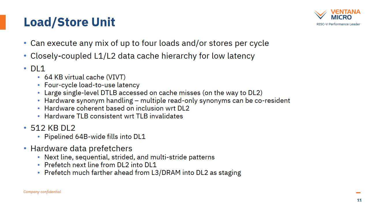
However, Ventana is looking to avoid these shortcomings by tracking address space IDs alongside L1D tags. That lets them avoid flushing the L1 data cache on context switches. Furthermore, the L1D can handle cases where multiple virtual addresses map to the same physical address. Perhaps V1 can record a certain number of VA to PA aliases in the L2 TLB, and invalidate all of those aliases in one go if a snoop shows up.
V1’s L1D still has four cycle latency, much like AMD and ARM’s recent CPUs. They’re not getting any latency benefit out of using a virtually addressed L1D, but they do avoid the power and area overhead of maintaining a L1 DTLB. Ventana got a lot of questions over their use of a VIVT cache, but I think they’ll be fine. They’ve clearly put work into avoiding the worst of a virtually addressed cache’s issues. Even if it ends up seeing a higher miss rate than an equivalent VIPT L1D, L2 hit latency is relatively low at 11-12 cycles anyway.
Execution Engine
We’re used to seeing CPUs with a lot of execution ports. That’s because different execution ports are specialized for different operations, and enough execution ports have to be available for the different mixes of instructions a CPU will encounter. Ventana has instead chosen to use fewer, more flexible ports. The Veyron V1 has four combined integer and memory execution ports even though the rest of the pipeline is eight-wide. Intuitively, core throughput would be held back by lack of execution resources.
However, execution resources are rarely fully utilized in a sustained fashion even if the frontend has more than enough width, because throughput in today’s high performance CPUs is typically held back by memory latency. Sandy Bridge is an example of a CPU with relatively low port counts. While it can sometimes see port contention, that happens because certain workloads stress execution units that are behind a particular port, instead of the CPU running out of execution ports in total.

Veryon is therefore looking to reduce power and area usage by having four well utilized integer pipes, instead of more poorly utilized ones.

While Veyron’s execution port layout definitely turned some heads at Hot Chips, I don’t think it’s particularly unusual. Other CPUs reduce execution port count by having ports serve different instruction categories too. Intel has long placed floating point and integer execution units behind the same port. Two ports on Fujitsu’s A64FX serve both AGU and ALU functionality. Benefits of this approach are clear too.
[Zen 4’s vector register file] had only minimal growth since register file area is mostly limited by the width and number of access ports, and not so much the number of storage cells per entry.
Kai Troester at Hot Chips 2023, on Zen 4’s AVX-512 implementation
More ports mean either more scheduling queues, or beefier schedulers that can pick multiple operations per cycle. Register file area is another concern. More execution unit stacks mean more register file ports are needed to feed them. Avoiding this area growth is a smart move.
Area
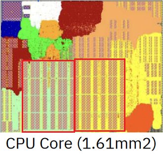
Area is a priority for Ventana, because they’re aiming for high core counts. Area efficiency also helps lower costs. Veyron V1 is smaller than AMD’s Zen 4c and ARM’s Neoverse V2. Ventana’s area-conscious design decisions play a role in this, but Veyron V1 trades performance to reduce area usage too. It doesn’t have vector execution capability, with only a scalar floating point pipe. AMD’s Zen 4c has very high vector and FP throughput in comparison. Against Neoverse V2, V1 has less L2 caching capacity. Ventana has undoubtedly achieved good core area efficiency, but its unconventional design choices aren’t a game changer, at least with regards to area.
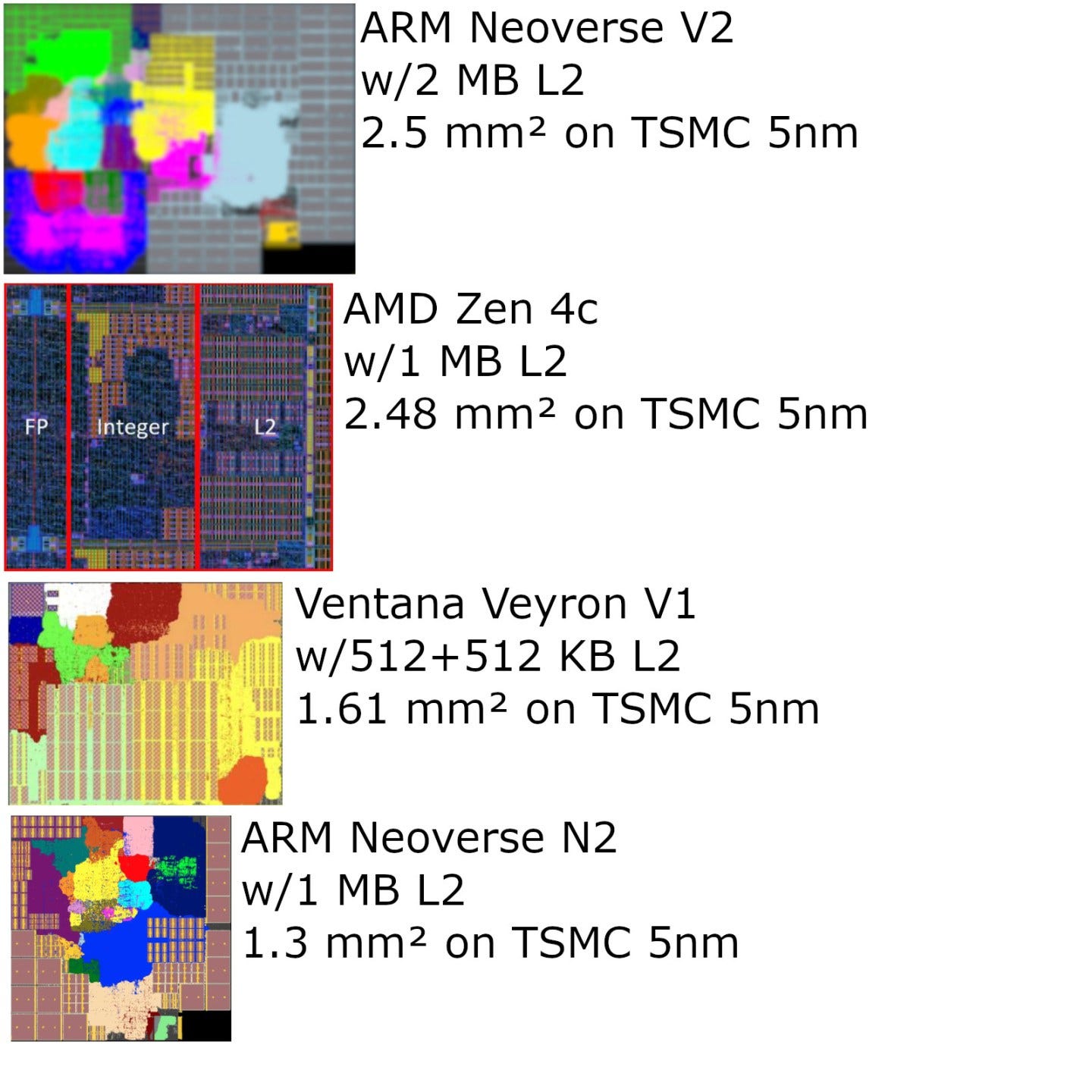
ARM’s Neoverse N2 is another interesting comparison. It’s not as wide as Veyron V1 and has smaller BTBs and TLBs. V1 could very well perform better in integer code, especially if that code has a large instruction-side memory footprint. But N2 has advantages too, like a very basic 2×128-bit vector execution setup.
Cluster Area
Core area is only one part of the equation. Recent client and server CPUs spend substantial amounts of area on supporting logic like interconnects and caches. AMD’s Bergamo is a particularly interesting comparison, because Ventana aims to scale to high core counts using a similar hub and spoke chiplet setup. That is, Veyron V1 and Zen 4c both use compute chiplets attached to a central IO die.

Ventana has provided images of a 16 core Veytron V1 cluster in their Hot Chips presentation, along with area figures on TSMC’s 5 nm process. AMD has also provided a photo of a Zen 4c 16 core CCD in their presentation. For area comparisons, I’m using Fritzchens Fritz’s 69.49 mm2 figure for Zen 4’s CCD size, and assuming Zen4c’s CCD occupies similar area.
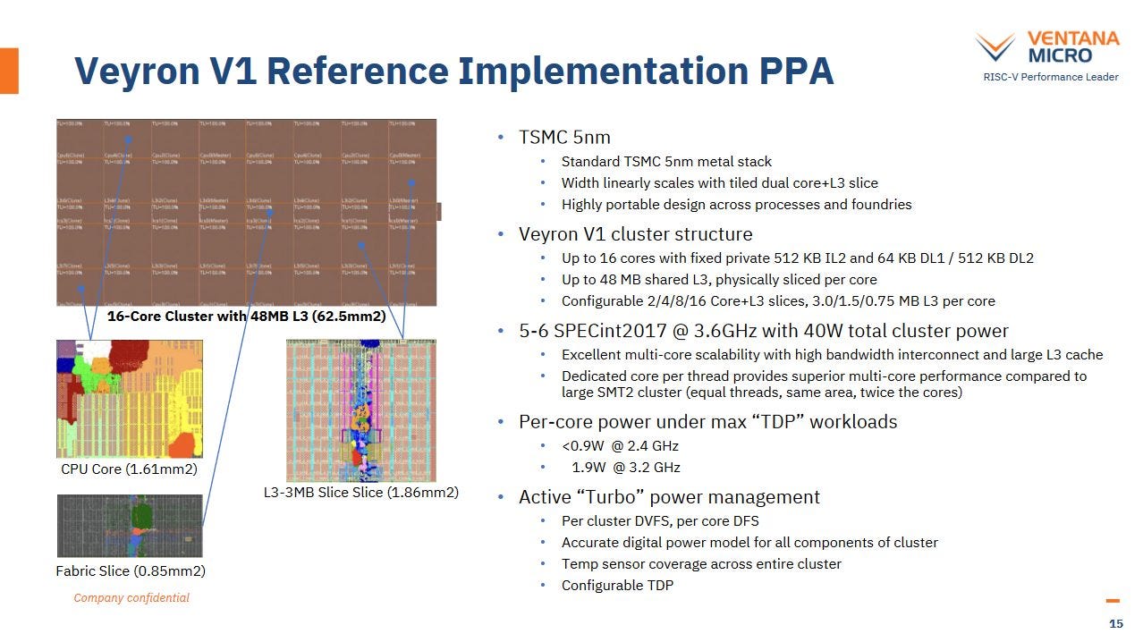
At first glance, 16 Veyron V1 cores with caches and supporting interconnect logic has a slight area advantage over AMD’s Bergamo. However, a close look at the die shot shows that Ventana hasn’t included die to die interfaces in their images. Such interfaces would occupy significant area.
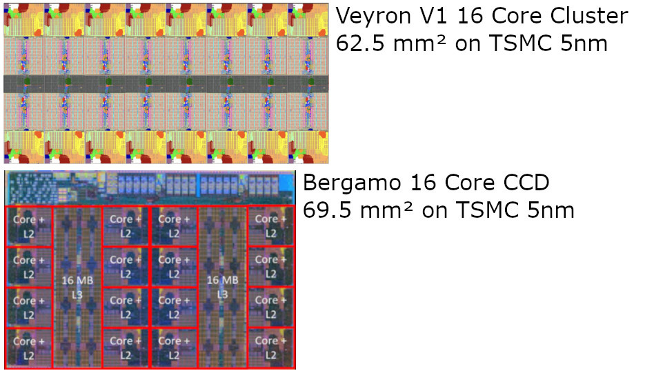
Therefore, Veyron V1’s compute chiplet size is probably not far off of AMD Bergamo’s. Veyron V1 enjoys more L3 cache capacity at 3 MB per core, compared to AMD’s 2 MB per core. Ventana’s intra-cluster interconnect also covers 16 cores and their associated L3 slices, providing 48 MB of L3 capacity to any core. In AMD’s favor, their Zen 4c cores have a more flexible unified L2 cache and much stronger floating point and vector execution.
Intra-Cluster Interconnect
Ventana uses a ring-like interconnect. Their slide says there are dual rings, but 160 GB/s of bisection bandwidth at 2.5 GHz would mean 64 bytes per cycle. If the ring can move 32 bytes per cycle, then there’d only be one ring and we’d be looking at transfers on both sides of it.

Perhaps it is a dual ring setup, and the ring can only move 16 bytes per cycle. I’m not exactly sure what Ventana’s interconnect looks like here, but ring-based setups tend to provide reasonably good L3 performance. Hopefully Ventana has executed well here, because their split 512+512 KB L2 design may mean the L3 sees more traffic than on designs with a 1 MB unified L2.
Final Words
V1 has a set of very unique design decisions. Deviating from the norm is risky because engineers have figured out what works and what doesn’t over the history of CPU design. That’s why successful CPUs share a lot of common design features. Ventana looks to have done a reasonably good job of making sure they didn’t fall into any obvious holes. They’ve mitigated VIVT cache shortcomings with hardware synonym handling and ASID filtering. Their split L2 design has enough caching capacity on both the instruction and data side. Their large, single level BTBs and TLBs either have low enough latency to not hold back performance, or are placed away from the most performance critical paths.

Even though Veyron V1 is a first generation design from Ventana, it’s likely a competent contender for scalar integer applications. Ventana will have a much harder time on throughput bound applications. V1 has no vector capability, and even if V2 does, the RISC-V ecosystem is even less mature than ARM’s. Software will have to be written to support RISC-V’s vector extensions. There’s a ton of throughput bound software out there, from video encoders to renderers to image processing applications. They’re maintained by a lot of different people with different priorities, so new instruction set extension support tends to move slowly. ARM already faces a software support struggle as it tries to establish itself as a viable alternative to x86, and RISC-V faces an even greater challenge in that area.
We’d like to thank Ventana for putting together a very nice presentation on their Veyron V1 core, and look forward to seeing what the company does with their upcoming V2 design.
If you like our articles and journalism, and you want to support us in our endeavors, then consider heading over to our Patreon or our PayPal if you want to toss a few bucks our way. If you would like to talk with the Chips and Cheese staff and the people behind the scenes, then consider joining our Discord.