
Deep Diving Neoverse N1

Our previous article gave a pretty narrow view of how Neoverse N1 and Zen 2 stacked up, and mostly focused on whether ISA was responsible for performance differences. Here, we’re going to analyze Neoverse N1 in more depth, on both the micro(architecture) and macro level. We’re still going to use Zen 2 as a reference point, but we also benchmarked a lot of other chips for perspective.
Let’s start with N1’s microarchitecture.
Neoverse N1 Architecture Deep Dive
Cache and Memory Bandwidth
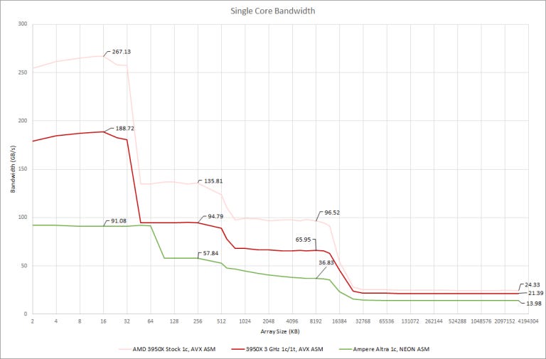
At all memory subsystem levels, the 3950X can give a single thread more bandwidth per clock than Neoverse N1. We got 31.59 bytes per cycle out of Zen 2’s L2, compared to 19.28 bytes/cycle on N1. 19.28 bytes/cycle is higher than 16, suggesting that Neoverse N1’s L2 interface is 32 bytes wide. However, N1’s L2 design has difficulty getting close to theoretical bandwidth.
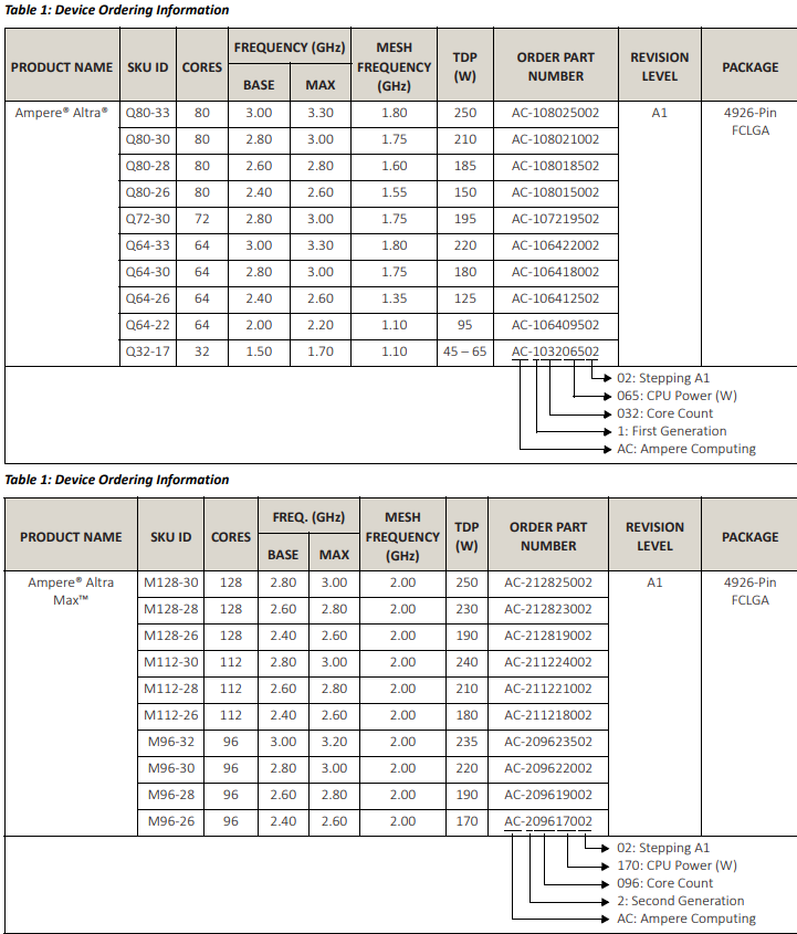
Zen 2’s L3 cache provides far more bandwidth than Ampere Altra’s. It even beats Altra’s L2. This is likely because AMD puts the L3 cache very close to the cores and runs it at core clock. In contrast, Ampere Altra uses a mesh clocked at 1.8 GHz to enable a large monolithic design. ARM’s CMN-600 mesh interconnect can technically hit 2 GHz, but Ampere only reached that mesh clock on new 128-core variants:
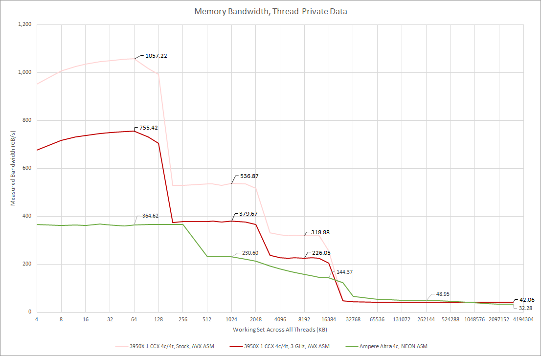
With 4 threads, Ampere Altra’s L2 catches up to Zen 2’s L3, but is behind for all test sizes until the 3950X runs out of L3. Altra has a slight bandwidth advantage when going out to memory, though that advantage fades as test size increases. At 3 GB, Zen 2 takes a small lead even with fewer memory channels.
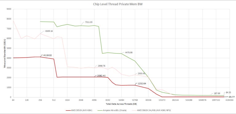
Moving over to the full chip, Ampere Altra has a huge advantage over the 3950X and 3960X. Unfortunately, we don’t have a 64 core Epyc to test. But 80 cores are hard to beat if you can use them all, and that’s what Altra was made for.
Now, let’s have a look at all-core L3 bandwidth. We didn’t use the same memory bandwidth test that we used in the Zhaoxin article, because both the 3950X and Ampere Altra give unreasonably high results when the test moves into DRAM. I’m guessing the memory controllers are combining requests from different cores that go to nearby addresses. To give accurate memory bandwidth figures, we used a separate array for each thread to stop the memory controller from combining accesses. Unfortunately, that makes Ampere Altra’s 32 MB L3 invisible next to 80 MB of L2, so we’re bringing the previous version back to find Altra’s L3.
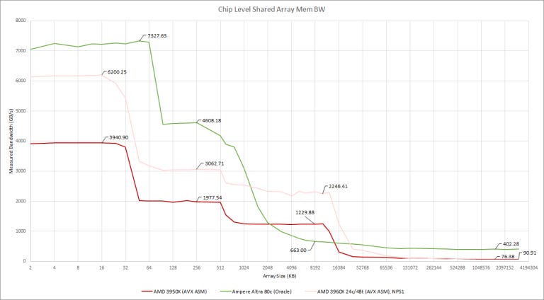
Results still aren’t clear, but our best guess is that L3 bandwidth is around 663 GB/s – well under Zen 2’s in Threadripper configuration. Funny enough, even a desktop 3950X chip has more total L3 bandwidth than Altra. In fairness to Altra, L3 cache bandwidth doesn’t seem to be important outside of some scientific applications.
If you head over to our memory latency data page, you’ll see that Altra’s L3 has over twice the latency of Zen 2’s (3950X or Epyc 7452). This is why I personally think AMD won’t put a L4 or system level cache on the IOD. Such caches are too small, high latency, and low bandwidth to be useful.
TLB and Pagewalk Performance
In modern operating systems with multitasking, user programs don’t directly access physical memory locations. Instead, applications use virtual memory addresses that the CPU translates to physical ones. To speed this up, CPUs cache translations in structures called TLBs, or translation lookaside buffers.
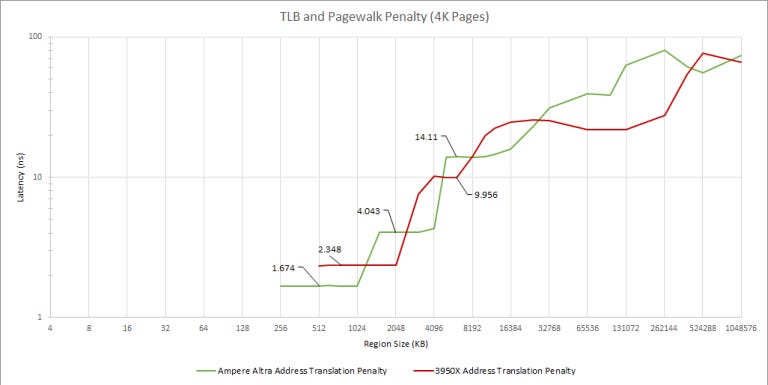
Zen 2 has a larger L1 data TLB, with 64 entries compared to Neoverse N1’s 48. The L2 TLB on N1 is also smaller, with 1280 entries compared to Zen 2’s 2048. But N1’s has lower latency (5 cycles) than Zen 2’s (7 cycles). Beyond that, results are hard to interpret. Zen 2’s optimization manual says it has a 64 entry page directory cache that can hold page-map-level-4 and page-directory-pointer entries. I couldn’t find any equivalent documented for N1.
Branch Prediction, Analyzed Further
Direction Prediction, in 2D
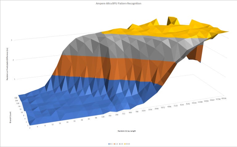
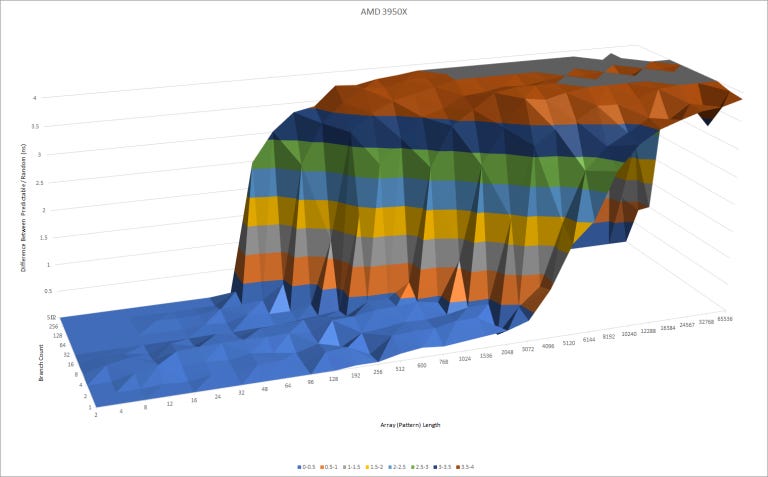
Both Neoverse N1 and Zen 2 have advanced direction predictors. But Zen 2 can recognize longer patterns and handle more branches. While this test isn’t meant to directly measure pattern history table size, it suggests that Zen 2’s BPU has a lot more storage for pattern tracking than N1’s.
But this comes at a cost. As pattern lengths get longer, Zen 2’s second level TAGE predictor overrides the first level more and more. That causes pipeline bubbles in the frontend, which show up as gradually increasing latency here. Interestingly, both TAGE predictor and L2 BTB overrides are counted with Zen 2’s “L2 BTB Overrides” performance monitoring event. Maybe the L2 BTB and TAGE predictor generate their results in the same pipeline stage.
Indirect Branch Prediction
Indirect branches can go to more than one target. That adds another dimension to branch prediction difficulty, because the predictor must determine which target the branch will go to. This is a relatively new addition to our test suite, and from our results, Neoverse N1 has a larger indirect predictor than Zen 2.
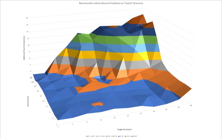
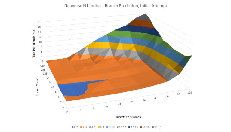
N1’s able to track at least 4096 indirect branch targets (512 indirect branches with eight targets each). The indirect predictor on N1 is also faster than Zen 2’s. There seems to be very little penalty as the test cycles through more targets per branch, until N1’s indirect target tracking capabilities are exhausted.
N1 seems to lose indirect predictor capacity when direct branches are added to the test loop, hinting that direct and indirect branches may share a BTB.
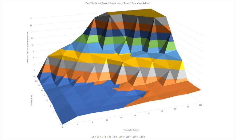
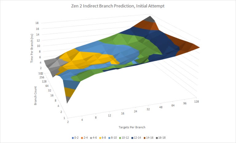
On the other hand, Zen 2 can track at least 128 targets per branch for up to two branches. For sure that’s very impressive, but Zen 2 can’t track more than 1024 total indirect branch targets. Also, Zen 2’s indirect predictor suffers more latency as target count increases. The optimization manual says the indirect predictor “chooses among [indirect branch targets] using global history at L2 BTB correction latency”. While that latency penalty isn’t heavy, having a lot of targets per branch is going to hurt Zen 2’s frontend throughput more than N1’s (unless you have just a couple indirect branches with an insane 128 targets each, which N1 will mispredict).
Finally, Zen 2 appears to only use taken/not-taken global history to predict indirect branch targets. If the testing loop only has indirect branches and a loop branch (neither of which have taken/not taken history correlated with target selection), Zen 2 mispredicts a lot. Other CPUs like Neoverse N1, Skylake, and funny enough, Piledriver, either use local history or include indirect target selection as part of global history. I’m not sure how much difference it makes in the real world, since Zen 2 doesn’t seem to suffer a lot of indirect branch mispredicts, but it certainly complicated testing.
Return Stack
Returns are a special case of indirect branches. Prediction is a lot easier because they (usually) come in call+return pairs. On a call instruction, the instruction pointer is pushed onto a return stack. And on a matched return, it’s popped off the stack to provide a prediction.
N1 an interesting return stack implementation:
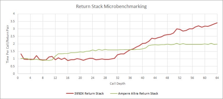
Like Zhaoxin, Neoverse N1 has a two level return stack. Unlike Zhaoxin, N1’s L1 return stack is reasonably deep with 11 entries, with an additional 31 entries in a second level. This second level is a bit slower, but nowhere near as horrifyingly slow as Zhaoxin’s. Meanwhile, Zen 2 opts for a fast, single level return stack with 31 usable entries.
Rename/Allocate Stage Optimizations
A lot of modern CPUs can optimize certain instructions as they’re being sent to the execution engine, allowing it to extract more IPC. For example, register to register moves can be eliminated by renaming two ISA registers to the same physical one. The rename stage can also recognize operations that never need to wait for inputs to be ready, like xor-ing a register with itself to zero it.

Neoverse N1 and Zen 2 can both collapse dependencies between MOVs, but N1’s can’t eliminate MOVs and often fails to remove dependencies between them. Zen 2 has a far more robust mechanism that “executes” every register-to-register MOV in the rename stage with zero latency.
N1 recognizes that moving an immediate (encoded right into the instruction) value of zero to a register sets it to zero, and handles that without needing an ALU pipe. However, it doesn’t recognize any other case we tested. Zen 2 can recognize more cases where instructions are independent, but doesn’t completely eliminate them because throughput doesn’t exceed ALU port count.
Block Diagram
Wikichip has a somewhat complete block diagram based on ARM’s published info, but some details are missing. So we tried to fill the gaps with microbenchmarks. To save space, we won’t go over stuff in depth if it’s captured in the block diagram.
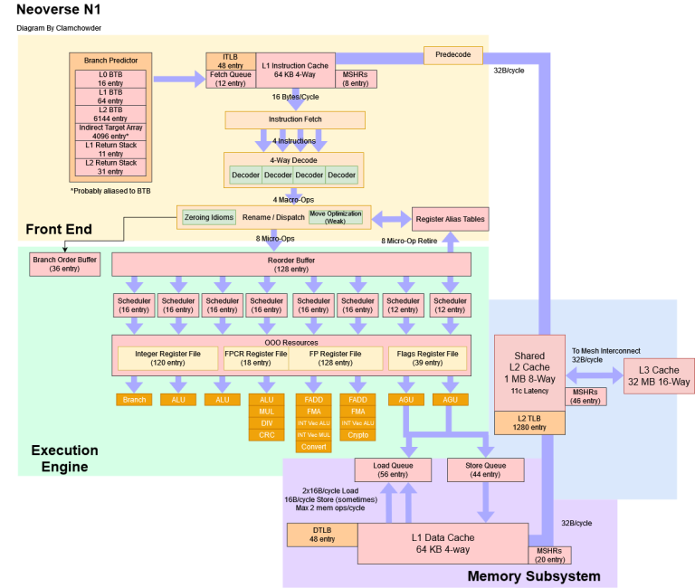
Fetch queue depth, rename/allocate width, and commit/retire width come from the Neoverse N1 Platform White Paper. We used microbenchmarking to determine the other structure sizes. The white paper also says the instruction cache stores partially decoded instructions. That simplifies post-L1i decode logic at the cost of storing extra metadata in the L1i. ARM doesn’t specifically say how much overhead there is for N1, but their documentation says prior ARM designs used 36 to 40 bits for every 16 or 32-bit instruction.
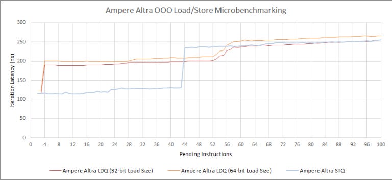
For load and store queue sizes, our test results disagree with Wikichip’s figures. N1 clearly cannot extract instruction level parallelism past 44 stores or 56 loads. It also struggles with just two pending loads between cache misses, even if those loads are always L1D hits.
And here’s a Zen 2 block diagram for comparison:
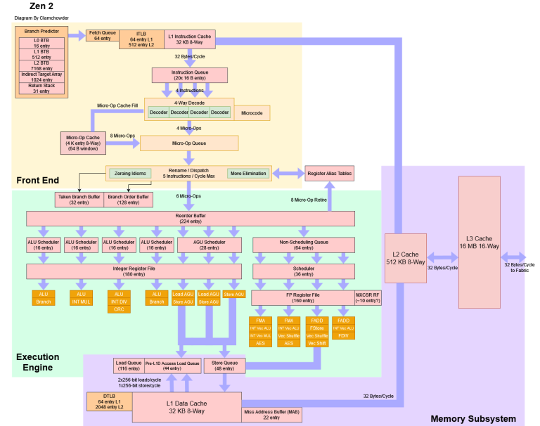
AMD’s optimization guide for Zen 2 says its load queue has 44 entries. From our microbenchmarking, this 44 entry figure only applies to loads waiting on data. If the loads speculatively complete and are just waiting to retire, Zen 2 can track 116 of them. For those who are curious, Neoverse N1’s load queue would have 37 entries if we use the same standard:
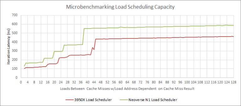
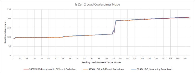
If we use the same load queue test we used for N1 above, Zen 2 can track up to 116 loads. This isn’t a load coalescing trick – we see the same result even if we send every load to a different 64 byte cacheline:
(Macro) Benchmarks
On the benchmark end, we going to check out the following:
Test with a single CCX config using a Linux VM, instead of the WSL and 1+1+1+1 config we tested before. Originally, we were going to investigate whether different CCX configurations would impact our conclusions, but that turned out to be pretty boring as 2+2 and 1+1+1+1 results landed within margin of error. And, Hardware Unboxed found no difference between 2+2 and 4+0 in a set of gaming tests on Zen 1.
WSL compared to a Linux VM was a bit more interesting, because it actually changed conclusions in one benchmark.
Show some data with SMT on. SMT is a fundamental feature of Zen 2’s architecture and is present on most product SKUs.
Test with Epyc, to evaluate performance with a server IOD. While it’d be great to get a bare metal comparison between AMD Epyc and Ampere Altra, that’s unfortunately out of reach. We’re a batch of hardware enthusiasts, not a big review site with substantial resources and connections. However, I did briefly spin up a 4c/8c Zen 2 VM in Azure (I’m a MS employee, and get Azure credits from the MSDN subscription that comes as a FTE benefit). It’s far from a good comparison point, but it does offer interesting perspective.
Large Project Build – Compiling Gem5
We’ll start with the biggest change. For the previous article, we ran the compilation workload from WSL1, assuming the overhead of translating system calls would probably be measurable but not large enough to swing conclusions. Testing on a Linux VM showed the previous assumption was wrong.
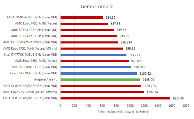
At matched clocks, Neoverse N1 takes 40.3% longer than Zen 2 to finish the compilation job. Compared to Zen 2 in an Epyc cloud instance, N1 took 27.2% longer. Skylake no longer suffers a loss, even when locked to 3 GHz. Clock for clock, Neoverse N1 is closest to Haswell and comes in 4% behind. With this new data, we have to reconsider our previous conclusion that Neoverse N1’s compilation performance was “impressive considering N1’s smaller core design.” It’s more accurate to say that N1’s performance was slightly underwhelming, landing two to three generations behind Zen 2 and about a generation behind Skylake.
If SMT comes into play, the 3950X wins by a whopping 86.4%. And with SMT, Haswell wins by 21%. Epyc 7452 takes 10% longer than the 3950X at 3 GHz, so code compilation is probably sensitive to memory latency.
File Compression
This is a difficult one. For the last article, we used Ubuntu’s p7zip-full package, or 7z version 16.02. The closest version available for download as a Windows binary was 16.04. We used 16.04 to test different CCX configurations, but the absolute results are weird. Despite achieving identical compression efficiency, the 16.04 7z Windows binary was dramatically faster.
To make things even more complicated, Linux VM results were slower than WSL ones. 7z results from the Zen 2 based Azure instance were more in line with those from the native Windows binaries, so we’ll be drawing conclusions with the Windows figures. Otherwise, Zen 1 ends up being 18.5% faster than Zen 2. And Epyc 7452 would beat the 3 GHz 3950X by 65%. Neither of those figures make sense, which indicates virtualization overhead with Hyper-V on Windows 10 is messing with results. But we’ve included the Linux VM numbers here anyway, for completeness.
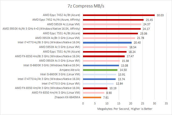
Clock for clock, desktop Zen 2 is 66.7% faster than N1. That’s a huge performance difference, and Zen 2 owes its larger than expected lead to a variety of factors:
Better branch prediction, with 97.6% accuracy and 5.35 mispredicts per 1000 instructions (MPKI). N1 achieved 95.6% branch prediction accuracy with 8.16 MPKI.
89.8% op cache hitrate, which is on the high side.
Larger data-side TLBs. Zen 2 suffered 2.02 L1 DTLB MPKI, compared to N1’s 2.77. So N1 suffered an address translation penalty about 37.1% more often than Zen 2. N1 also seemed to have more L2 TLB misses than Zen 2. N1 page-walked 0.74 times per 1K instructions, while Zen 2 missed the L2 DTLB 0.1 times per 1K instructions.
Altra’s L3 may as well be nonexistent. Perf counters showing under 1% hitrate. I wonder if the counters are just inaccurate though.
In N1’s favor, its larger L1D did well. It achieved 98.7% hitrate and 3.53 MPKI versus 98.9% hitrate and 4.33 MPKI on Zen 2. The hitrates are not a typo – more of Zen 2’s instructions accessed memory (43%) compared to N1’s (27.32%). That’s why it’s important to not look at hitrate alone. But that seems like a drop in the bucket compared to other factors.
Epyc 7452 beat the 3950X by 5%, probably because of boost behavior. Based on integer addition latency, the Epyc 7452 seems to boost to around 3.3 GHz. Unfortunately, there’s no way to lock cloud VM clocks.
Intel suffers in this test, probably from a worse branch predictor. Skylake only ends up 4% faster than N1, while Haswell falls 5.5% behind.
Rendering with Blender (Cycles)
The 3950X gains a bit of performance when run from a Linux VM, widening its lead over N1 to a massive 69.3% at matched clocks. While N1 put up a really good fight against a 3 GHz locked i7-4770 in compression and code compilation, Haswell pulls ahead by 37.2% here. Zen 1 squeezes in 10.1% ahead of N1, showing that there’s more to vector units than just the 128-bit width.
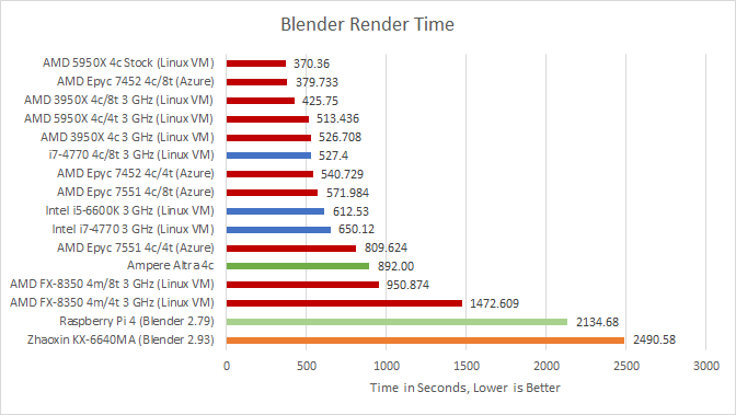
Zen 2 Epyc results are strange. It loses to the 3950X when both have 4 threads in play with 1 CCX. But wins with SMT enabled against the 3950X in a 2+2 configuration. And while we’re not focusing on Zhaoxin today, its poor AVX implementation does it no favors. It loses to Piledriver, and even a Raspberry Pi 4.
Public Key Crypto
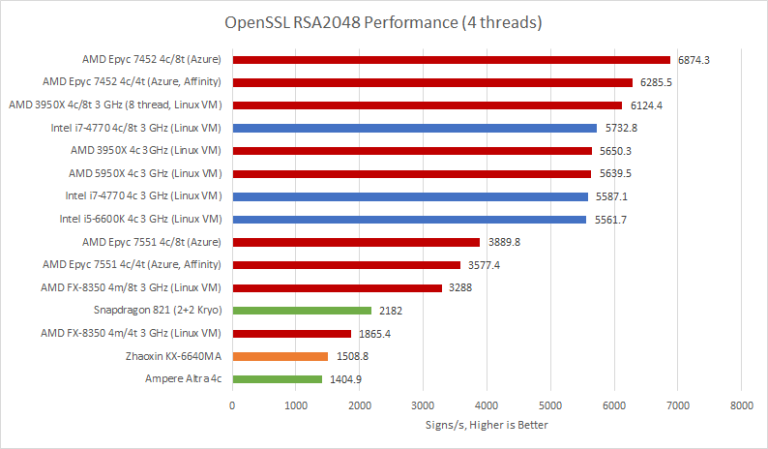
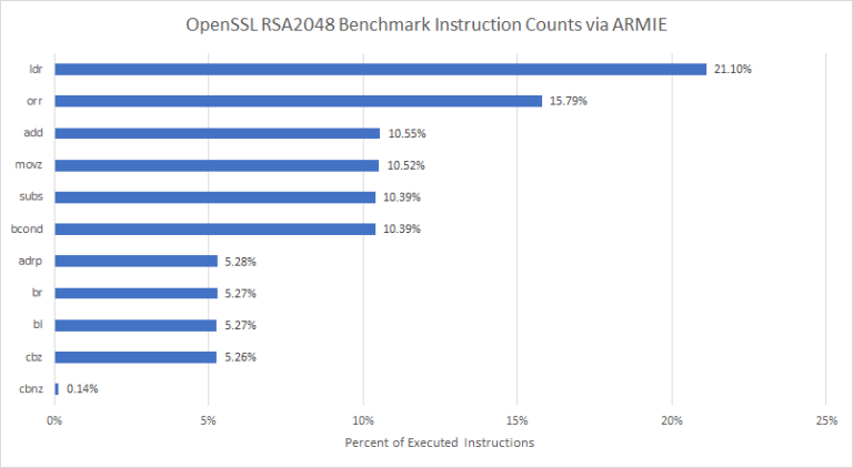
Results don’t change for asymmetric crypto. It’s a pure integer throughput test, which means WSL1 overhead doesn’t come into play. Again, N1 suffers heavily in this test. It loses to Qualcomm’s Kryo, showing that ISA doesn’t matter. Clock for clock, it’s also falls behind AMD’s aging FX-8350. That’s not where Neoverse N1 wound up in our other integer benchmarks. Whenever we see a strange result, it’s always good to dig deeper. So, we tried to see what instructions were executed during that OpenSSL benchmark:
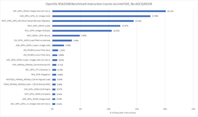
Add-with-carry instructions dominate here. Integer multiplication shows up a lot too. I haven’t thoroughly tested Kryo, but it has four ALU pipes and averages 1.25 integer multiplies per cycle, suggesting two multiply pipes that aren’t perfectly pipelined. Neoverse N1 achieves 1 multiply per cycle and has 3 ALU pipe. None of that explains Kryo’s 55% lead while running at lower clocks.
Unfortunately, N1 doesn’t have extensive performance monitoring counters like Intel and AMD CPUs. We can only see that the backend is stalling the renamer/frontend, but not what’s filling up in the backend or what pipes are being used.
Finally, we tried building OpenSSL 3.1.0 from the latest master to see if any new aarch64 optimizations were there. But OpenSSL 3.1.0 and 1.1.1 scores came within margin of error.
Looking beyond N1, we see some interesting patterns. There’s almost no difference between Zen 2, Zen 3, Haswell, and Skylake when all are running at 3 GHz, indicating that the integer execution units used by this test are pretty similar on all of those architectures. Zen 2 gains only 8.3% from SMT, which isn’t much compared to other applications. In fact, only the FX-8350 sees large gains from “SMT”, likely because its integer execution resources double with a second thread active.
Microarchitecture Simulation: ChampSim
Recently, we used a modified version of ChampSim to see how giant caches affect IPC. Now, here’s ChampSim in benchmark form, running a single trace in a single thread for 60 million instructions:
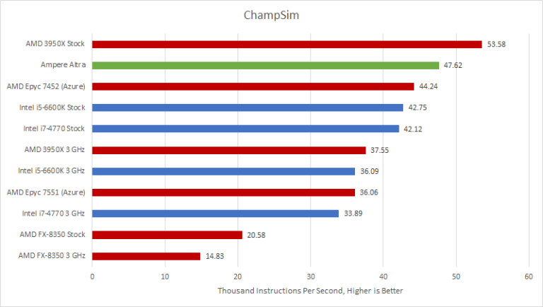
Neoverse N1 is impressive here. In this benchmark and only this benchmark, N1’s branch predictor did extremely well and suffered fewer mispredicts per instruction than any other CPU. Clock for clock, N1 is 26.8% ahead of Zen 2, and 31.9% ahead of Skylake.
N1 owes its ChampSim win to excellent branch prediction accuracy and better L1i hitrate. Its branch prediction was 98.86% accurate with just 2.65 MPKI, versus Zen 2 with 97.67% accuracy and 5.36 MPKI. From performance counters, N1 also got an incredible 99.7% L1i hitrate, versus 93.37% on Zen 2. AMD should consider bringing back K10 and Zen 1’s 64 KB L1i.
Video Encoding: libx264
The desktop x86 chips got a slight boost from using a Linux VM. Conclusions don’t really change compared to last time, but again we have more data points.
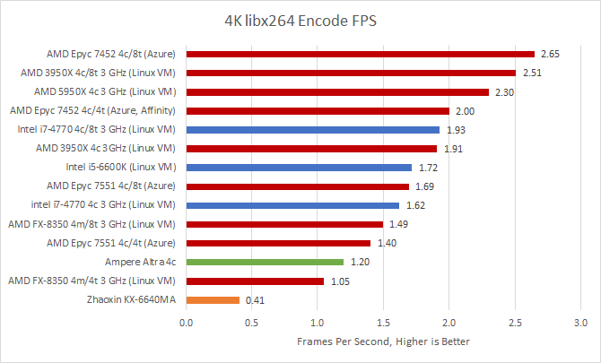
N1 falls well short of contemporary x86 cores. Or rather, Zen 2 shows off its vector units for a 59% lead. Similarly, Skylake leads by 43%. As for older architectures, Haswell manages to beat N1 by 35%, showing that Intel’s 2013 AVX implementation remains quite strong even today. On AMD’s side, Zen 1 is 17% ahead of N1, even though both use 128-bit wide SIMD units.
Epyc 7452 pulls a slight lead against the 3 GHz 3950X. Latency plays less of a role than clock speed for libx264.
Video Encoding: libx265
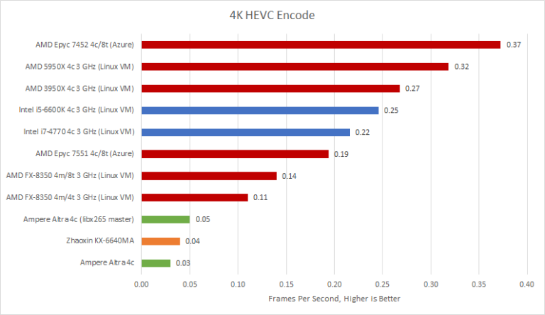
Rerunning with a Linux VM and single CCX configuration doesn’t change the picture. Everyone is miles ahead of N1 except Zhaoxin’s Lujiazui, which has a very weak vector implementation and lower clock speed.
Benchmark Analysis
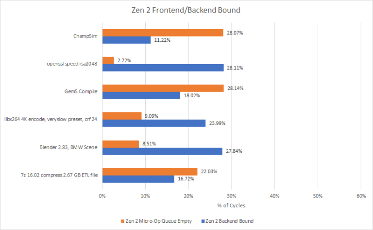
N1’s performance is best explained by its relatively small out-of-order execution engine, combined with poor cache performance beyond its 1 MB L2. Its rename/allocate stage spends a huge fraction of cycles stalled, waiting for backend resources to become available:
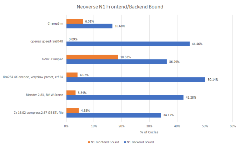
Zen 2 is still more backend bound on average, but the situation is a lot less extreme:
To their credit, ARM has beefed up the backend in A77 and A78. They also made large frontend changes by adding a micro-op cache, though I suspect that had limited impact. The micro-op cache can provide more instruction bandwidth, but N1 needs a better backend to take advantage of that. The micro-op cache could reduce average branch mispredict penalty too. But the N1 already had a fairly short pipeline thanks to its low clocks and predecode mechanism. Anything helps, i guess.
On Zen 2’s side, AMD could benefit by improving both the frontend and backend. Zen 3 did exactly that. But there’s still room to improve by using a bigger L1 instruction cache.
Conclusions and Closing Thoughts
Core for core and clock for clock, Neoverse N1 is not a match for Zen 2 regardless of CCX configuration or platform. Those variables change performance by a few percent, which doesn’t shift conclusions when Zen 2 is often multiple generations ahead.
Haswell is a much better comparison. It ends up very close to Neoverse N1 in integer workloads (excluding outliers like OpenSSL and ChampSim). At first glance, that’s not bad. Just eight years ago, Haswell was the gold standard for desktop performance, and a lot of Haswell CPUs are still in use today. But by locking the i7-4770 at 3 GHz, we’re making it compete with one hand tied behind its back. At stock, Haswell would be significantly faster.
Worse, N1 gets cut down in benchmarks that use Haswell’s vector units. That highlights a big problem with using source-based benchmarks like SPEC. Throughput bound programs like video encoders and renderers often use intrinsics or assembly to take advantage of ISA features. By ignoring that, source based benchmarks give an unrealistic picture of real world performance.
Finally, let’s take a brief look at where Ampere and AMD are going in the near future. On AMD’s side, Zen 3 based Epyc chips (Milan) are getting rolled out. Milan’s core count doesn’t increase, but the Zen 3 architecture brings significant per-core performance gains. Meanwhile, Ampere has been busy rolling out a 128-core Altra variant, which still uses Neoverse N1 cores. While we don’t have one to test, Anandtech saw decreased per-core performance. That’s expected, since Ampere cut down the L3 cache to 16 MB and reduced clock speeds.
Ampere and AMD are certainly moving in different directions, with different goals in mind. But I wonder what would have happened if Ampere used ARM’s newer A77 or A78 architectures instead of spamming more N1 cores. N1 was introduced in February of 2019 according to Wikichip, which means it’s more than 2.5 years old. That’s a long time in the world of CPUs, especially when you’re coming from behind.
If you like what we do, please consider heading over to our Patreon to toss us a few bucks so that we can continue to give you guys this type of content.
Methodology Notes and Setup
We turned to a Hyper-V Linux VM with 4 cores to test a 1 CCX configuration. At first, we tried to use affinity masks to force Windows to schedule workloads on one CCX. Unfortunately that ran into a ton of problems. Some applications like Blender and ffmpeg (libx265) did not respect affinity settings, and probably overrode them. WSL1 loads were not affected by affinity at all.
That’s where the VM comes in. AMD’s Zen 2 chips can communicate preferred cores to the OS via a mechanism called CPPC (Collaborative Performance and Performance Control).
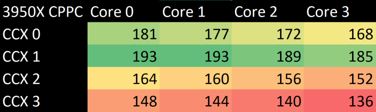
Luckily, the highest ranked cores on the 3950X were all on CCX 1, so Hyper-V consistently put a quad core VM’s load on that CCX. During testing, I watched task manager to make sure load didn’t go to other cores. On the 5950X, the second CCD was disabled, creating a 1 CCX config.
For SMT tests, the 3950X was set to a 2+2 configuration, since it’s impossible to only enable one CCX on the 3950X.
Other setup details for non-cloud tests:

Unfortunately, it’s impossible to determine memory configuration on cloud VMs.