
Loongson’s 3A5000: China’s Best Shot?


We at Chips and Cheese have covered two Chinese CPU architectures: Zhaoxin’s x86 compatible Lujiazui architecture found in the KX-6000 series of CPUs and Phytium’s ARM compatible FT663 architecture found in the D2000 series of CPUs. Zhaoxin was founded in 2013 as a joint venture between VIA and the Shanghai Municipal Government. Phytium was founded in 2014, and appears to use a Cortex A72-derived architecture in their FTC663. Both are thus relatively new efforts in China’s domestic microprocessor push.
In this article, we’re going to cover Loongson’s 3A5000, the latest in a much longer line of domestic Chinese architectures. The 3A5000’s LA464 architecture traces its lineage back to the GS464 core, which grew out of the 10th Five Year Plan. This plan funded domestic microprocessor efforts via the 863 Program among others. For much of the GS464’s lifetime, development happened under the Institute of Computing Technology (ICT) at the Chinese Academy of Sciences. ICT has a very long history going back to 1956, and handled numerous projects of national importance like supercomputer construction and training computer researchers.

GS464 saw numerous improvements over the years. The 11th Five Year Plan aimed to get higher performing domestic Chinese CPUs and DSPs, and initiated the HGJ project. ICT responded by dramatically increasing structure sizes, though the core continued to be called GS464. Towards the end of the 11th Five Year Plan, the core was passed to the newly founded Loongson Technology Corporation Limited. However, at least some of the same people continued to work on the GS464 processor line, as the same names appear on subsequent research publications (like 胡伟武, or Weiwu Hu).

That sets the stage for the 12th Five Year Plan, which aimed to promote “the application of Chinese domestic CPUs and DSPs”4. Under these goals, Loongson produced a radiation hardened 100 MHz CPU that was used in the BeiDou satellite. Of course, general purpose CPUs were on the menu as well. GS464 by now suffered from poor branch prediction and memory performance. To cope, Loongson began development on the GS464E architecture, based on research from IBM’s POWER7, Intel’s Ivy Bridge, and ARM’s Cortex A9. The GS464E appears to form the basis of the LA464 core we see today in the 3A5000.
The 3A500’s LA464 core moved from MIPS to Loongson’s in-house architecture, known either as LoongISA or LoongArch. Today, Loongson wants the 3A5000 to target everything from PCs to servers to embedded applications. We’re going to take a deep look at the architecture, and see how it tries to fulfill that promise. Of course, we’re also going to compare it to some AMD, ARM, and Intel architectures.
Many of our microbenchmarks depend on assembly code. Compilers tend to do unpredictable and complicated things that make it difficult to observe architectural characteristics from high level code. Unfortunately, that means we had to write a lot of code to look into Loongson’s 3A5000. Writing assembly can be hard, and writing assembly for an unfamiliar ISA (LoongArch64) brings difficulty to another level. Testing microbenchmark code isn’t easy either. Normally, we can validate tests by running them on a CPU with known characteristics and making sure the results are sane. But Loongson’s 3A5000 is the only LoongArch64 CPU we have, and most details are not public. The chance of error is high, so keep that in mind throughout the article.
Block Diagram
The LA464 is a 4-wide out-of-order architecture with modestly sized buffers. In some places, it has modern features like physical register files and wide vector execution. But that doesn’t apply everywhere. Overall, it’s a very distinctive architecture, with design decisions we haven’t seen in other cores.
Frontend: Branch Prediction
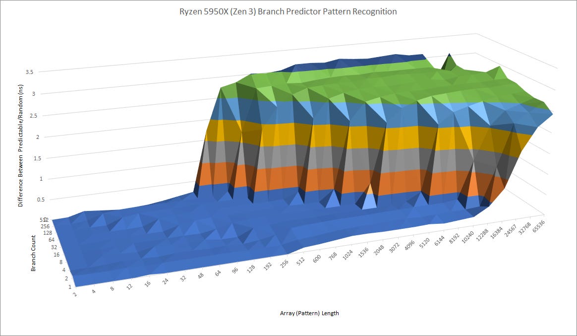
A CPU’s pipeline starts at the branch predictor, which determines where to fetch instructions from. Branch predictor performance is absolutely critical to achieving high performance. Sending the pipeline down the wrong path will cause wasted work, and taking too long to determine a fetch target could starve the pipeline. Branch prediction accuracy on the 3A5000 appears to be quite decent, and is able to hold its ground against Zen 1 and Ampere Altra in 7-Zip. It falls behind a bit in libx264, but isn’t too far off.
Direction Prediction
The GS464E uses a tournament-style predictor, where a meta-predictor chooses whether to use local history or global history for a prediction. For the uninitiated, local history refers to whether the branch was taken before, and global history refers to whether prior branches in the instruction stream were taken. The local history table, global history table, and selection table all have 16384 entries on the GS464E, making it quite large compared to the classic tournament predictor implemented in DEC’s Alpha 21264. AMD’s Bulldozer uses a tournament predictor as well, and AMD’s optimization guide implies Bulldozer’s global history table also has 16384 entries.
The LA464 possibly uses a similar predictor. If we test how well the branch predictor does with increasingly long random patterns, the Loongson turns in a mediocre performance. It’s nowhere near what current Intel and AMD CPUs are capable of. Recent Intel and AMD CPUs have used TAGE or perceptron predictors, which can achieve higher accuracy with less predictor storage.
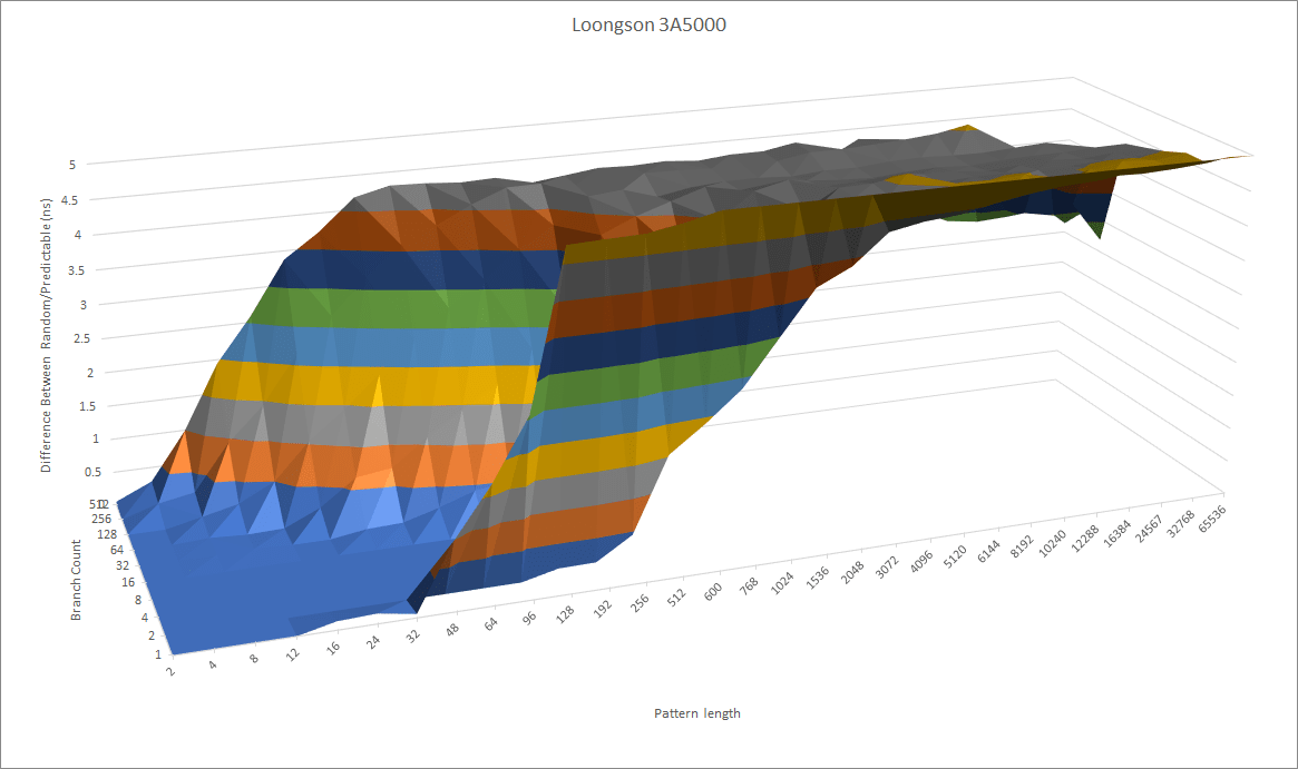
Without branch prediction of the same caliber, Loongson will struggle to get performance to scale well with a bigger core. Bigger core buffers for keeping more work in flight won’t help much if you keep having to throw out incorrectly fetched instructions. A predictor of Bulldozer or Loongson’s caliber may be adequate for a core with 128 ROB entries, but times have moved on and Loongson will need something better to keep pace.
Branch Predictor Speed
A branch predictor’s ultimate goal is to speed up branch handling. Predicting where the branch will go is important of course, but doing so quickly can be just as critical. If your branch predictor takes too long to steer the frontend, you could end up starving the pipeline of instructions. To speed things up, Loongson has a 64 entry BTB (Branch Target Buffer, a cache of branch targets). If a branch target comes out of this BTB, the frontend doesn’t have to stall at all.
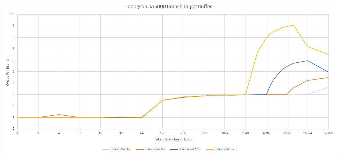
If branch footprints spill out of the 64 entry BTB, the CPU has wait for the branch to be fetched from L1i and then calculate the target address. At that point, taken branch latency is basically L1i latency, which appears to be three cycles on the LA464. For comparison, recent Intel and AMD CPUs only have a latency of one or two cycles even when handing thousands of branches. This latency is especially painful because the 3A5000 clocks much lower than AMD or Intel’s chips, so branch latency in actual time is quite high.

Loongson’s scheme avoids the area cost of a large L2 BTB, but prevents the branch predictor from following the instruction stream after a L1i miss. CPUs from Intel, AMD, and ARM can maintain high instruction throughput for large code footprints by using the branch predictor to drive prefetch from the instruction side. While this technique was new in the Sandy Bridge and Bulldozer days, it’s common knowledge today and implemented even on low power architectures. Not seeing it in Loongson is really like a blast from the past.
Indirect Branch Prediction
Branches that go to multiple targets are harder, because the branch predictor has to pick between branch targets too. These tricky branches are also called indirect branches, because they tell the CPU to jump to an address in a register instead of directly encoding the target. For a single indirect branch, the 3A5000 can track about 24 targets before running into penalties (probably mispredicts). We see around 512 total indirect targets tracked without significant penalty, with 256 branches and two targets per branch.

This level of indirect branch handling capability is decent. It’s quite appreciated as well, because object oriented programming languages tend to use indirect branches to handle method calls. But it’s not as capable as that of other recent CPUs.

Neoverse N1 deserves mention, because it’s also a core with modest performance targets. But ARM was able to to implement indirect branch prediction capabilities that aren’t far off that of Zen 3 and Golden Cove. Loongson is significantly behind.
Return Prediction
Returns are a special case of indirect branches, because they typically show up in matched call/return pairs. Many CPUs therefore keep a stack of return addresses. On a call, they push an address onto the stack. To predict a return, they pop an address off the stack. Loongson has given the 3A5000 a 32 entry return stack, which should be adequate for the vast majority of cases. This is a notable improvement over the GS464E, which had a 16 entry return stack.

AMD’s Zen 2 has a similarly sized return stack, and is often able to achieve over 99% return prediction accuracy.
Frontend: Instruction Fetch
Once the branch predictor has determined where to go, the frontend has to bring instructions into the core. That’s where the instruction side cache hierarchy comes in. To start, 3A5000 has a large 64 KB 4-way L1i. This is nice to see, especially when top end CPUs from AMD and Intel have settled on smaller 32 KB instruction caches.

However, it looks like the large L1i is meant to mitigate Loongson’s poor performance when fetching code from L2 and beyond. Zen 1 and Skylake are both able to sustain 4 IPC when pulling instructions from L2, and still do very well even if they have to run code out of L3. Loongson cannot match that and could become capped by frontend bandwidth for larger code footprints.

Strangely, code fetch bandwidth from L2 is worse than from L3. I wonder if Loongson ran into some difficulties when implementing hardware instruction cache coherency. If done correctly, hardware instruction cache coherency can benefit JIT-ed code and enable better scaling to high core counts. However, it’s not easy. Loongson’s L2 is non-inclusive, which means it can’t act as a snoop filter. Maybe a L2 hit from the instruction side has to probe the L1D to ensure it gets up-to-date data. But a L3 hit might benefit from separate coherency directory located in the L3 complex, which can indicate whether up-to-date data can be provided without snoops.
Renamer
After instructions are fetched and decoded, the renamer has to allocate resources in the backend to track them. Alongside the obvious task of register renaming to break false register name dependencies, the renamer can also pull certain tricks to expose more parallelism to the execution engine. Recent Intel and AMD CPUs can do this in spades, with register-to-register moves and zeroing idioms handled in the renamer for free.
Loongson doesn’t have any such optimizations as far as I can tell. The renamer does what you’d expect from what a computer science course tells you it should do, and that’s about it.
Out of Order Execution
Absorbing cache and memory latency is key to maintaining high performance, and Loongson has a decently sized out-of-order engine to do that. In terms of size and ambition, it looks vaguely comparable to Neoverse N1’s. Both have a 128 entry ROB, and similar register file sizes. N1 has a distributed scheduler, while Loongson uses a more unified scheduling queue configuration with fewer total entries.
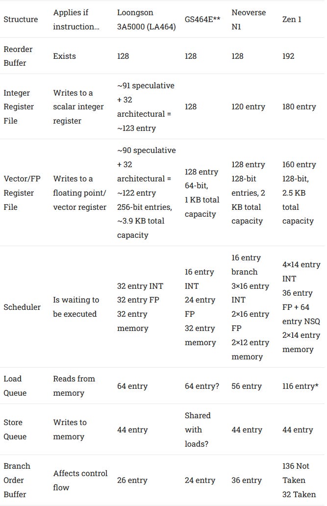
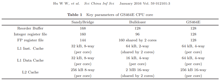
Compared to the older GS464E core, LA464 maintains the same reorder buffer and register file sizes, but Loongson has beefed up the all-important scheduler sizes. The GS464E already had decently sized register files for a CPU with 128 ROB entries. LA464 should be able to make even better use of its 128 entry ROB. But recent AMD, Intel, and even ARM CPUs are way ahead of Loongson. They have even larger reorder buffers, with other structures getting increases as well to keep the core balanced.
Loongson may have opted for conservative structure size increases in order to increase clock speeds. Given a choice between increasing IPC by doubling structure sizes (as the GS464E did to the GS464), and increasing overall performance by increasing clock speed, the latter is definitely a better choice. However, western companies were able to increase clock speed while also increasing structure sizes, leaving Loongson in the dust.
Integer Execution
In a previous article we covered vector execution, so if you want to know more about the FPU on the 3A5000 then go read that article. Now it’s time to look at the scalar integer side of the Loongson 3A5000. Loongson’s LA464 core dramatically increases integer throughput compared to the GS464E, with four ALU pipes instead of two. Prior GS464E derived cores always looked a bit funny, with two ALUs in a 4-wide core. In fairness, the cores in each Bulldozer module are 4-wide but only have two ALUs, but that’s a specific case that emphasizes multithreaded performance with a shared frontend.

While Loongson has massively improved on the GS464E, their current core does have a few shortcomings on the integer execution side. LA464 can only resolve one branch per cycle, even if the branch is not taken. This capability is equivalent to what ARM’s Neoverse N1 or Intel’s Sandy Bridge could do. But newer Intel and AMD CPUs can sustain two branches per cycle, usually providing at least one of them is not taken.

Loongson does have an advantage with integer multiplication throughput. Like Gracemont, the 3A5000 can do two scalar integer multiplications per cycle, while most other cores can only do one. Even with the low clock speed of the 3A5000, in absolute throughput it can exceed its ARM and x86 rivals from before 2020. However, this advantage is minimized when compared to the latest AMD and Intel desktop cores, which clock more than twice as high as the 3A5000. It’s further diminished by integer multiplication latency, which is mediocre at 4 cycles. That’s the same as AMD’s Phenom and Intel’s Core 2, which are more than two decades old and clocked higher than the 3A5000. Anything recent from Intel and AMD combine much higher clocks with lower cycle count latencies, putting them miles ahead.
Vector and Floating Point Execution
We previously looked at the 3A5000’s vector and FP execution layout, nothing that its capabilities were weaker than that of Zen 1 and Skylake. More details are in that article. But to summarize, Loongson has only two vector execution ports, and suffers from high FP execution latency. Floating point add, multiply, and fused multiply-add instructions execute with five cycle latency regardless of vector width. That’s the same latency as AMD’s RDNA 2 graphics architecture, which is funny because RDNA 2 also reaches similar clocks.
Vector integer operations are better, with single cycle latency for vector adds. Despite that, a quad core Ampere Altra cloud instance manages to edge out the 3A5000 in libx264 video encoding, thanks to a combination of higher clock speed and possibly a more extensive set of specialized instructions. Just like with the scalar integer side, the 3A5000 does have an advantage in being able to do two 256-bit vector integer multiplies per cycle, putting it on par with Skylake and outmatching Zen 1. But again, low clock speeds mean the 3A5000 is unlikely to match either in reality.
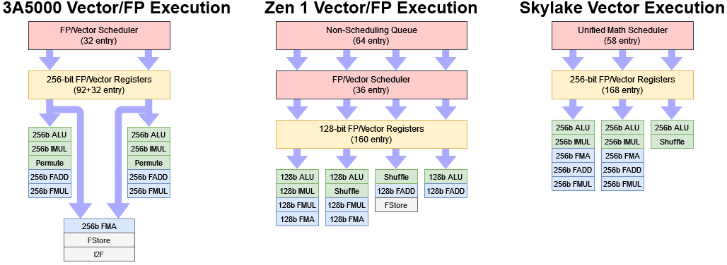
Comparing to Intel and AMD is just one side of the story. The older GS464E core had 64-bit FP units, placing it back in the x87 and MMX era. Loongson of course has to work off the base they’re given. While ICT was managing Godson development, they created the GS464V, a variant of the GS464 with powerful vector units for use in supercomputers. I suspect the GS464V forms the foundation of the LA464’s vector implementation. According to an IEEE paper, the GS464V “integrates two 256-bit-wide vector units in the core”, and the “vector ALU module is used twice”1.
Address Generation
Memory operations start executing at the address generation units, which calculate the memory address that a load or store operation wants to address, and passes that the load/store unit. The Loongson 3A5000’s LA464 core has two AGUs, letting it execute two memory operations per cycle. Both can be loads, and one can be a store. That makes it roughly comparable to Neoverse N1, Zen 1, and Sandy Bridge.

However, it’s a step behind Intel’s Haswell architecture and its successors, which can do two loads and a store in the same cycle. Current generation AMD and Intel CPUs also have massively expanded memory execution capabilities. For example, Golden Cove can do two loads and two stores per cycle. Zen 4 can do three memory operations per cycle, of which two can be stores. When Loongson developed the GS464E with Intel’s Ivy Bridge in mind, a two-AGU setup seemed perfectly fine. But times have moved on, and now it seems quite dated.
Load/Store Unit
Once virtual addresses are generated, they’re passed on to the load/store unit. The load/store unit makes sure memory dependencies are respected, and translates the virtual addresses into physical ones. To speed things up, Loongson can speculatively execute loads ahead of stores with an unknown address.
If a load does take data from an earlier store, Loongson can forward the store data with 7 cycle latency. Store forwarding works as long as the load is contained within the store, and the accesses don’t cross a 64B cacheline boundary. 7 cycles of store forwarding latency is not the best performance for a 2.5 GHz CPU. Zen 1 has the same store forwarding latency but clocks much higher, while Skylake can forward store data with 5 cycle latency (or, just one cycle over uncontested load latency).

Loongson acts a bit like Skylake, in that both do a coarse grained check. Loongson does so at 8B granularity, while Skylake does so at 4B granularity (i.e., comparing an extra bit). That means a load and a store can’t go in parallel if they both hit the same 8 byte block on Loongson, even if they don’t truly overlap. This 8B overlap penalty also applies across 16 KB pages. If the load and store touch the same 8B block at the same offset within different 16 KB pages, there’s also a false dependency. Finally, if a load partially overlaps a store, Loongson takes a 14 cycle penalty. That failed store forwarding penalty is not bad, and in line with what other CPUs see.
The load/store unit’s job gets harder if accesses cross a 64B cacheline, because that would involve two L1D accesses under the hood. Such accesses are called “misaligned accesses”, because they go across a L1D alignment boundary. Loongson handles misaligned loads by executing them over two cycles. That’s not out of line, though newer Intel and AMD CPUs don’t see any misaligned load penalty at all. Stores are far worse for Loongson, because a misaligned store takes 10 cycles. Old Intel CPUs from the Core 2 era did suffer similar penalties, but recent CPUs are generally much better. The 10 cycle penalty is quite hefty considering the CPU’s low clocks.
If an access crosses a 16K page boundary too, it’ll need two TLB lookups in addition to two L1D accesses. Loongson handles this case quite well, with the same misaligned load penalty, and the misaligned store penalty increasing to 15 clocks. Zen 1 takes a 24 cycle penalty, which comes out to almost the same actual time if Zen 1 runs at 4 GHz.
Address Translation
After generating addresses, the core has to translate virtual addresses (as seen by the program) to physical addresses that correspond to locations in DRAM. This translation allows the operating system to enforce permissions and provide each process with its own view of memory, ensuring that one misbehaving program won’t bring down the entire system. However, address translation creates overheads too. TLBs minimize that overhead by remembering those address translations.
Loongson translates addresses in 16 KB chunks, or pages, by default. For comparison, x86 and ARM CPUs typically use 4 KB pages. Loongson’s larger pages mean each TLB entry has more coverage. LA464 has a 64 entry L1 DTLB, which can cover 1 MB, backed by a 2048 L2 TLB for 32 MB of total TLB coverage. These large page sizes should give Loongson some advantage over its x86 and ARM counterparts.
Hitting the L2 TLB appears to add 2.3 ns of latency over a L1 TLB hit, or around 5-6 cycles. That compares favorably to Zen 1, which has 7-8 cycles of L2 TLB latency. However, Zen 1’s higher clocks mean it enjoys better actual latency.
Cache and Memory Access
Once the load/store unit has done its checks, it gets the requested data from the memory hierarchy. Like many modern CPUs, Loongson uses a triple level cache setup. All high performance CPUs today depend on caches because improvements in DRAM performance have not kept up with improvements in CPU core performance.
L1D Cache
Like previous architectures from the GS464 line, the 3A5000 enjoys a nicely sized 64 KB L1D. It is 4-way set associative to enable virtually indexed, physically tagged addressing with 16 KB pages. However, latency is a weak point. Four cycles might not sound bad, but at the 3A5000’s low clock speed, I expect better. AMD’s K10 architecture achieved 3 cycle latency at much higher clocks using older process nodes.

Effective L1D latency is made worse because Loongarch, like MIPS, lacks a scaled index addressing mode. Compilers end up generating extra instructions to calculate addresses for array indexing, dramatically increasing L1D latency. For comparison, x86-64 and aarch64 both have a scaled index addressing mode. At the most, using that capability incurs a 1 cycle penalty. On Loongson, GCC-compiled array indexing code sees a latency of eight cycles, which is brutal at 2.5 GHz.

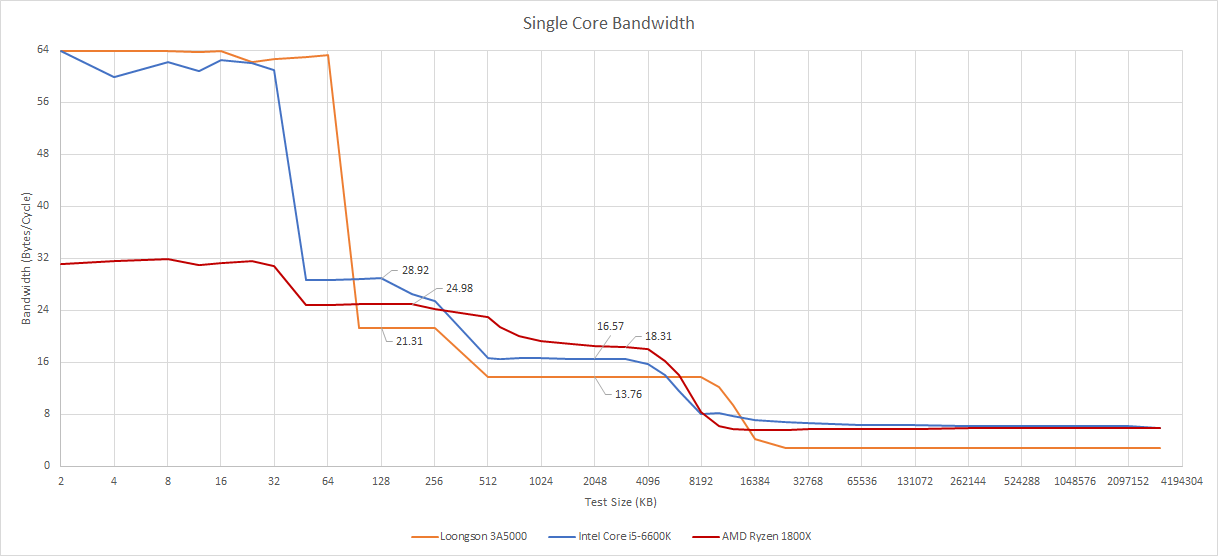
Bandwidth-wise, Loongson has set the L1D up to handle the demands of 256-bit vector execution. Using undocumented LASX instructions, we were able to do two 256-bit loads per cycle, or one 256-bit load and one 256-bit store. The 3A5000 therefore has better L1D bandwidth than Zen 1, even with AMD’s clock speed advantage. However, it’s no match for Skylake.
L2 Cache
Like many CPUs today, Loongson has a L2 mid-level cache that insulates cores from L3 latency. On the 3A5000, the L2 is 256 KB, 16-way set associative, and acts as a victim cache. L2 latency is mediocre at 14 cycles. Intel has been running 256 KB L2 caches at 12 cycle latency for the better part of a decade, and at much higher clocks to boot. If we look at actual latency, the 3A5000’s 5.6 ns is worse than the FX-8350’s 4.8 ns. Zen 1 is even faster than that, and still has more L2 capacity.

L2 bandwidth averages out to 21.3 bytes per cycle – not great, not terrible. That’s a tad worse than Skylake at over 28 bytes per cycle, or Zen 1 at over 24 bytes per cycle. Again, clock speed differences mean AMD’s and Intel’s old CPUs have a notable actual L2 bandwidth advantage over Loongson’s 3A5000.
L3 Cache
Loongson’s L3 is arguably one of the CPU’s best features, because it offers 16 MB of capacity for a quad core cluster with decent bandwidth and latency. The L3 functions as a victim cache, and is constructed out of four banks. According to the 3A5000’s user manual, the L3 and cores are connected via a “5×5 frequency division switch” using the AXI protocol. CPU cores are connected to the switch as masters, while the L3 cache slices act as slaves. Switch ports are set up to give each port 32 bytes per cycle of read bandwidth, and 16 bytes per cycle of write bandwidth.

The interconnect setup is likely carried over from the Godson 3 days, when ICT worked to implement the old GS464 core in high core count configurations. That’s not a surprise, considering the same people worked on the project even after it switched to Loongson ownership. However, Loongson has doubled the read bandwidth to each L3 slice.
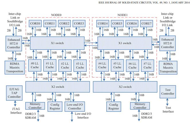
With four L3 slices, each capable of delivering 32 bytes per cycle, we should get 320 GB/s of theoretical L3 bandwidth at 2.5 GHz. We don’t get anywhere near that. Perhaps the cores can’t track enough outstanding L2 misses to absorb L3 latency. Perhaps there’s contention within the 5×5 switch. Perhaps the 3A5000 clocks the L3 cache below core frequency. After all, the Godson-3B1500 ran the cores at 1.25 GHz, but ran the L3 at 1 GHz.

Whatever the case is, AMD and Intel have a clear L3 bandwidth advantage. Zen 1 and Skylake can both pull more bytes per cycle from L3, and their high clock speed puts Loongson even further behind. Loongson does have a capacity advantage, but that disappears against more modern chips from both AMD and Intel.

In Loongson’s favor, at least they managed to implement an L3 that’s far better than Bulldozer’s. We see roughly linear L3 bandwidth scaling as thread counts increase. Scaling should be good as Loongson scales out beyond quad core configurations, because each L3 instance is private to a quad core cluster. Like with AMD’s Epyc, L3 bandwidth should scale linearly as more core clusters are added, unless there’s some sort of terrible mistake.
The L3 has around 40 cycles of load-to-use latency. In cycle counts, that’s not bad and similar to Zen 2. However, the absolute latency of 16 ns is quite unimpressive for a client design, and Loongson should really have a shorter L3 pipeline length for a CPU that runs at 2.5 GHz.

Loongson’s 3A5000 does compare favorably to the prior Godson-3B1500. The Godson 3 has about 50 cycles of L3 latency, from a paper published in IEEE. At 1.25 GHz, that would come out to 40 ns. 16 ns is worlds better, so Loongson should be commended for making progress.

If the 3A5000 misses L3, it accesses the DDR4 memory controller through a second-level AXI switch.
DRAM Access
From the graph above, the Godson-3B1500 has 160-170 cycles of memory latency, which works out to 128-136 ns. That’s not too bad for a dual channel DDR3-1066 configuration with RDIMMs. Unfortunately for the 3A5000, Loongson dropped the ball when going to DDR4. We measured 144 ns of memory latency using DDR4-2666. Loongson must have bought their memory controller from wish.com because it’s a flaming pile of garbage.
We’re testing with DDR4-2666, with both slots populated. The 3A5000 has a dual channel memory controller, which should give it theoretical bandwidth on par with consumer chips from five to six years ago. Theoretical is the key word here, because reality is different.

A single Loongson core can pull around 7 GB/s from DRAM, while all four cores together stop short of 14 GB/s. Each core would have to make do with just 3.37 GB/s of DRAM bandwidth in an all-core workload, making bandwidth limitations likely. This is an abysmal performance for a dual channel DDR4 setup, because it’s far behind even mediocre DDR3 configurations. For example, an i7-4770 with dual channel DDR3-1333 gets just over 19 GB/s.
The consequences of getting a bargain basement memory controller will vary. Everyday tasks like web browsing or word processing may be fine. Server programs, HPC workloads, image processing, video editing, and parallel code compilation may not be fine.
We should also remember that this is a quad core chip running at 2.5 GHz. Memory performance will become an increasingly severe problem as Loongson tries to go for higher clock speeds or higher core counts, because the compute to bandwidth ratio will get even worse. That applies on the latency side too. 144.5 ns is 361 cycles at 2.5 GHz, but 578 cycles at 4 GHz. In a way, the 3A5000’s very low clock speeds mask the worst of its memory performance issues.
Final Words
Loongson’s 3A5000 is the most promising domestic Chinese CPU we’ve seen so far. Compared to the Zhaoxin KX-6640MA and Phytium D2000, Loongson’s 3A5000 is a wide core with a better balanced backend and a better cache hierarchy. But it suffers the same fundamental issues as the other two in its quest to be a general purpose CPU. Loongson’s LA464 simply cannot deliver performance in the same class as any recent Intel or AMD architecture. Compared to its western counterparts, LA464’s architecture is smaller, the L2 and L3 caches are worse, and the DDR4 memory controller is embarrassingly bad. Even though Loongson has gotten their cores up from 1 GHz to 2.5 GHz, no one runs desktop or even laptop CPUs at clocks that low. Because of its massive clock speed deficiency, Loongson can’t even get in to the same performance ballpark as recent desktop CPUs. It even struggles against Neoverse N1 running at 3 GHz.
Loongson’s progress is also not promising. From microbenchmarking, the LA464’s architecture is basically a generation over that of the GS464E – a core from the early 2010s. GS464E was designed to get close to western cores from around that time in clock-for-clock performance. That’s a huge problem because even back then, Sandy Bridge and Bulldozer clocked significantly higher than LA464 does today. And of course, Golden Cove and Zen 4 are many, many generations ahead of Sandy Bridge.
The result is that today, Loongson doesn’t feel any closer to Intel and AMD than they were a decade ago. I also don’t think they have a good chance of landing in the same performance ballpark unless they make some giant leaps. Making a low power processor with passable performance is a lot easier than making a leading-edge CPU. Going for high performance means smacking out one bottleneck after another, and addressing those bottlenecks gets increasingly complex as you push the limits of CPU performance.
Software ecosystem is another issue. Ironically, the 3A5000’s ISA will make it less usable in practice, even though it’s stronger than the Phytium or Zhaoxin. Loongson noted that MIPS suffered from weak application support and a toolchain that wasn’t as strong as x86’s. Creating a new, incompatible instruction set that mostly reuses the MIPS toolchain is a hilariously stupid way to not solve that problem. And to add to that problem, Loongson split the LoongArch ABI into “Old World” and “New World” which are incompatible with each other. This just adds another level of stupidity to this mess of a software ecosystem.
As of 2022-07-18, all commercial LoongArch distributions are incompatible with all community distributions. All binary software built on community distributions, and some software written in high-level languages and existing in forms like source code or bytecode (such as those written in Python or Java) cannot run on commercial distributions, and vice versa. All closed-source software from ISVs such as WPS Office are built on commercial distributions, so they are extremely unlikely to work as-is on community distributions.
This is the so-called compatibility problem between the old-world and the new-world. Because the Loongson Corporation finished all commercial moves before announcing the LoongArch to the open-source community, the open-source LoongArch ecosystem is the new world; in contrast to this, all commercial distributions and the ecosystem associated make up the old world. The two worlds are to be united eventually, but are two parallel universes for now; and the technical difficulty of making the two worlds compatible with each other is enormous.
Loongson does have ISA extensions to aid binary translation for ARM, MIPS, and x86. But this is quite a complicated way of working around not using a more common ISA in the first place. We also didn’t have a lot of fun with binary translation on Loongnix (a Debian-based distro for Loongson). x86-64 Geekbench segfaults immediately. Minimizing performance loss from binary translation is cool, but not working is not cool. In fairness, the 32-bit x86 version does work under binary translation. But tons of programs are 64-bit these days, and you really need x86-64 translation to work. Even if it does work, binary translation will add overhead to an already low performance CPU.
In the end, Loongson’s LA464 is an interesting example of a low power, low performance architecture. The Loongson/ICT team has definitely been hard at work trying to achieve the goals set out for them. But their pace of innovation trails that of AMD and Intel, both of which have been relentlessly pushing the boundaries of CPU performance. But looking at LA464, and then looking at Zen 4 or Golden Cove provides perspective on just how impressively AMD and Intel have been pushing the boundaries of CPU performance. It also shows how the consistent progress by western companies has given China’s CPU makers an incredibly difficult moving target.
If you like our articles and journalism, and you want to support us in our endeavors, then consider heading over to our Patreon or our PayPal if you want to toss a few bucks our way. If you would like to talk with the Chips and Cheese staff and the people behind the scenes, then consider joining our Discord.
References
Weiwu Hu et al, An 8-Core MIPS-Compatible Processor in 32/28 nm Bulk CMOS, IEEE Journal of Solid State Circuits, Vol. 49, No. 1, January 2014
Weiwu Hu et al, Microarchitecture of the Godson-2 Processor
Weiwu Hu et al, Godson-3: A Scalable Multicore RISC Processor with x86 Emulation, IEEE Micro, December 2019
Weiwu Hu, Yifu Zhang, Jie Fu, An Introduction to CPU and DSP Design in China, Science China Information Sciences, October 2015