
China’s Phytium D2000: Building on A72?

China has been investing heavily into homegrown microprocessors for the past few years. Phytium’s D2000 is one example of a homegrown design, and we’ll be taking a close look at it in this article.
Phytium D2000 consists of eight FTC663 ARM cores running at 2.3 GHz, arranged in clusters with two cores each. The chip targets desktops, laptop, and industrial applications, which is a bit weird given its specifications. But to correctly evaluate this design, we have to keep the context behind its design in clear view. It’s not meant to go head to head with the best stuff AMD and Intel can offer. It’s meant to keep China going in case they seriously piss off a batch of countries that happen to be the ones making most of the world’s high end chips.
General Performance
When we covered Golden Cove, Gracemont, and other desktop architectures, we focused on architecture rather than absolute performance. Other outlets already do an excellent job of macro-benchmarking, so readers would already have a good idea of how an architecture performed relative to its peers when reading our work. Phytium D2000’s situation is different though. We’re not aware of a full benchmark review elsewhere, so we’re going to take a short detour, run a few workloads, and provide context on where D2000 stands. Keep in mind these results aren’t directly comparable to our past results, since we’re running everything on bare metal Linux this time.

Since Phytium includes desktops in their target market, we’re going to include Intel’s Core i5-6600K. This Skylake based chip represents a midrange desktop CPU from 2015. With a dated architecture, only four cores, and a pedestrian 3.6 GHz all-core boost clock, it’s easily smacked around by desktop CPUs available today. But on its own, it’s still a very usable platform that’s reasonably responsive for a wide range of desktop applications.
7-Zip
First, let’s look at file compression performance with 7-Zip. We’re simply timing how long it takes to compress a large file, instead of using the built in benchmark. 7-Zip’s benchmark mode will load as many cores as you can give it, but compressing a single file won’t scale as quite well with increasing core counts. In terms of instruction mix, 7-Zip is a very branchy workload that consists almost entirely of scalar integer instructions. It also has a small instruction footprint that fits within most L1 instruction caches, and enjoys a high micro-op cache hitrate.

Phytium does poorly, landing well behind the Core i5 despite fielding twice as many cores. It barely manages to squeak past a quad core Ampere Altra cloud instance, showing how strong Neoverse N1 cores are. Conversely, it shows how weak Phytium’s FTC663 architecture is. As we’ll see later, the FTC 663 architecture has one of the worst branch predictors we’ve seen in a modern out-of-order design. That does it no favors in this test, where over 15% of executed instructions are branches.

If we look at achieved IPC, Phytium ends up dead last. Phytium’s situation is even worse if we consider its low 2.3 GHz clock. Typically, IPC increases as clocks go lower, because DRAM accesses cost relatively fewer clocks, but that doesn’t help Phytium much.
Compilation (Gem5)
Let’s look at compilation performance next. Gem5 is a simulator used for microarchitecture research, and we’re going to see how long it takes to compile. Gem5 has a large codebase with a very parallelizable build process.

Even though all the CPUs here were pegged at 100% usage during most of the compilation process, Phytium’s eight core D2000 gets wrecked by quad core CPUs. It does manage a decent lead over Graviton 1’s Cortex A72 cores.

Looking at IPC, we can see how strong Skylake and Neoverse N1 are. Phytium also doesn’t beat A72 by a whole lot when we look at IPC. Strangely, Graviton 1 and Ampere Altra’s performance counters showed they executed more instructions than Phytium did.
libx264
Unlike the previous integer workloads, libx264 encoding loves CPUs with strong vector units and enough cache bandwidth to feed them. On Haswell, which has the same vector instruction set support as Skylake, over 40% of executed instructions belong to MMX, SSE, AVX, or AVX2. Unlike the integer workloads above, there are relatively few branches.

libx264 doesn’t infinitely scale with core count, but it does scale very well past four cores. Despite that, Phytium again fails to catch quad core Skylake and Neoverse N1. Remember, those represent a seven year old desktop CPU, and a roughly two year old server chip that has no intention of competing in the desktop market where per-core performance is essential.

Performance counters show Skylake and Neoverse N1 achieving massively higher IPC than Phytium. Skylake actually retires more than twice as many instructions per cycle on average, which is quite impressive considering around 13.89% of instructions it executed handle 256-bit vectors. Phytium’s weak branch predictor isn’t a giant handicap in this test because there aren’t too many branches to deal with in the first place. But now, Phytium’s weak vector execution capabilities are on full display. Neoverse N1 doesn’t have particularly strong vector execution units and is similarly held back because it has to use NEON instructions, while Skylake can use AVX2. Still, four Neoverse N1 cores manage a comfortable lead over eight FTC663 cores.
Minecraft
Minecraft, also known as block game, is a popular Java based application. Here, we’re testing how fast the Minecraft server can start up from scratch.

Again, Phytium gets destroyed. Intel’s Core i5-6600K gets the minecraft server started in less than half the time.
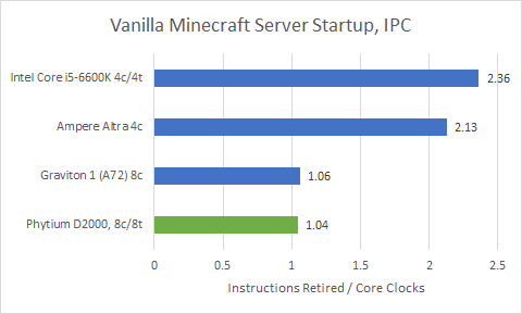
Turning again to performance counters reveals that Minecraft server startup is a very high IPC task. N1 and Skylake both average well over two instructions per cycle, and are making good use of their core width. Unfortunately, Phytium’s FTC663 cores get nowhere near that.
OpenSSL
Finally, we have RSA2048 asymmetric crypto – specifically, signs per second. This workload is more applicable to servers handling incoming SSL/TLS connections, but it’s interesting to see anyway. It’s a pure integer workload that heavily stresses a CPU’s scalar integer execution units, and just about nothing else. Unlike symmetric crypto, it can’t take advantage of any specialized cryptography acceleration instructions.

Phytium’s performance is suspiciously close to Cortex A72’s. Finally, we see Phytium’s eight cores beat a quad core competitor, but only because N1 seems to bottleneck on whatever integer operations OpenSSL uses here. Skylake better represents your average server core, and blows Phytium away.
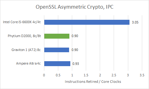
Performance counters don’t tell us anything we didn’t know already. Skylake is a monster here.
Phytium says the D2000 is “a high-performance general-purpose processor for desktop applications”, but its performance profile is about as far away as you can get from that of a desktop CPU. Desktops run client workloads, obviously, and those tend to not scale with increasing core counts as well as server and HPC workloads. Instead, client workloads are generally very sensitive to per-core performance – something that Phytium doesn’t have.
If you wanted to get a usable desktop CPU today, you could get a Core i5-6600K for under $50 from the used market and have a pretty decent experience. If you wanted to make a brand new desktop CPU as quickly and effortlessly as possible, you would do better grabbing four off-the-shelf Neoverse N1 cores and shoving that into a chip. It wouldn’t be anything to write home about, but it would still offer a client computing experience far superior to what Phytium delivers.
Now that we’ve established where Phytium’s D2000 sits with respect to performance, let’s head back to our regularly scheduled programming and deep dive the architecture.
Architecture
From a mile up, FTC663 is a 3-wide microarchitecture with out-of-order execution. It’s smaller than desktop architectures, including those from a decade ago. FTC663 bears a striking resemblance to ARM’s Cortex A72. The two architectures definitely aren’t the same, but if someone told me FTC663 was an evolution of ARM’s architecture, I would believe them. Looking at A72 and FTC663 feels a lot like looking at two generations of Intel cores.

Here’s ARM’s Cortex A72 for comparison, as implemented in Amazon’s Graviton 1:

Frontend: Branch Prediction
Good branch prediction is vital to any design with high performance goals. Phytium seems to have put some effort into this, because several years ago, they talked about a TAGE predictor in their Xiaomi cores. TAGE predictors have also seen use in AMD’s Zen 2 and possibly some Intel architectures, and involves indexing into several tagged predictor components with increasing history lengths. Typical implementations have extremely long maximum history lengths. FTC663 likely uses a variation of this, as it can handle longer history lengths than Cortex A72. But there’s a catch.
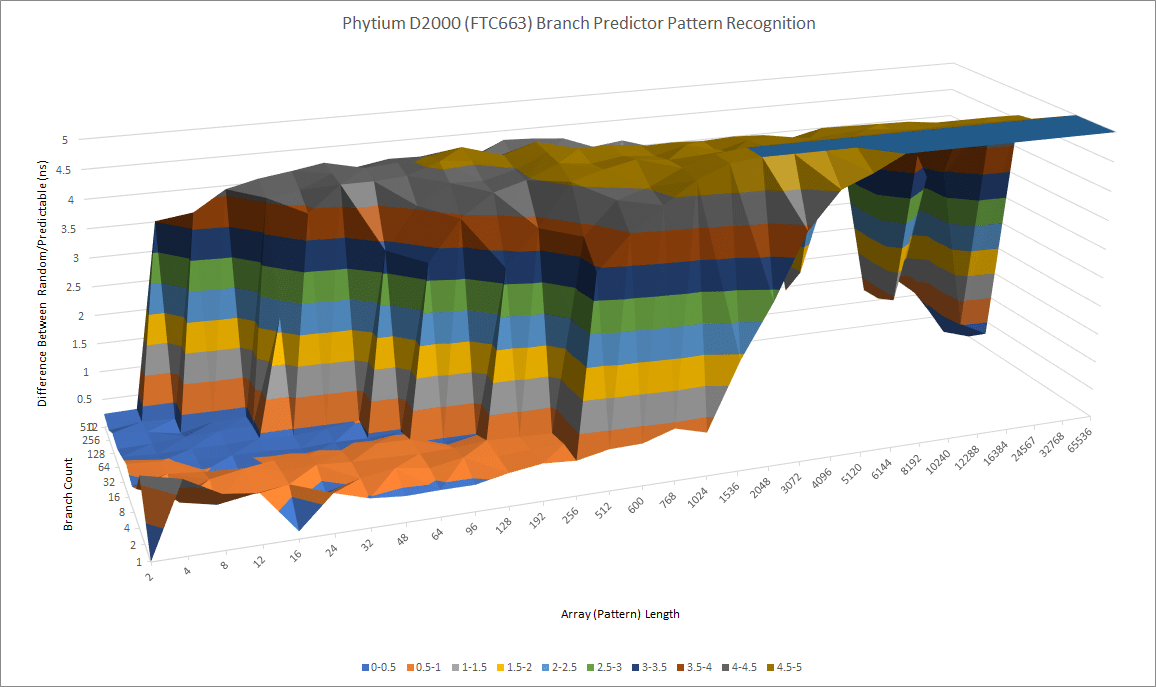

When a lot of branches are in play, FTC663’s predictor struggles more than A72’s. Phytium may have very little storage for branch history, or suffers from aliasing issues due to a poor choice of index bits for its branch prediction structures. If there are just a few branches that require very long history tracking to accurately predict, Phytium should be better. But if there are a lot of branches that can be accurately predicted with moderate history lengths, A72 might win.
Compared to Skylake and Neoverse N1, FTC663’s direction predictor is completely outclassed. Both feature much better predictors that can recognize very long patterns, and while holding up better when more branches are involved.


Let’s turn to performance counters to see how well Phytium did. FTC663’s predictor falls well short of Skylake’s and N1’s, which isn’t really a surprise. But surprisingly, FTC663 struggles next to the Cortex A72. That’s really bad, because Cortex A72 has one of the worst predictors we’ve seen in a remotely modern OoO core. FTC663 has deeper reordering capacity than A72, but performance improvements from that are sure to be blunted by more frequent mispredicts.

Take Gem5 code compilation for example. Branch mispredict penalty is typically around a dozen cycles, so suffering 11-12 branch mispredicts every 1000 instructions means well over 100 cycles wasted while executing those instructions.
Phytium knows that branch prediction is important, of course. After all, they put some effort into designing what looks like an advanced direction predictor. Getting to Skylake or Neoverse N1 levels of prediction accuracy likely wasn’t in the cards since FTC663 is a smaller core with lower performance goals. But Phytium seems to have made mistakes while tuning the design, and made incorrect tradeoffs that put them further behind than they probably would have liked.
BTB Speed and Capacity
Prediction accuracy is important, but a good predictor should deliver branch targets quickly as well. Otherwise, frontend throughput will suffer due to wasted cycles after taken branches. To supply branch targets with minimum latency, the predictor keeps a cache of branch targets, usually referred to as the branch target buffer (BTB).
Phytium’s BTB setup is dated and slow compared to modern cores. It closely resembles Cortex A72’s BTB setup – a 64 entry L1 BTB is backed by a 4096 entry main BTB tied to the instruction cache. Neither BTB level can deliver branch targets with 1c latency, meaning that the frontend will always waste at least one cycle after a taken branch. If a branch target comes from the L1 BTB, taken branch throughput is one every two cycles. If it comes from the main BTB, we see a taken branch every three cycles. This lack of “zero bubble” branch capabilitiy will make loop unrolling important for this processor.


Phytium’s BTB setup bears an uncanny resemblance to Cortex A72’s, right down to taking the same penalty if we set up branches that jump to the immediately adjacent instruction (branch per 4B). Branch density in this case is quite unrealistic, but it can show interesting things about how the CPU tracks branches. Cortex A72’s optimization manual actually hints at this:
Try not to include more than two taken branches within the same quadword-aligned quadword of instruction memory
ARM Cortex®-A72 Software Optimization Guide
I find it very amusing that advice from the Cortex A72 optimization manual can be so directly applied to Phytium’s FTC663.
Neoverse N1 and Skylake are both much faster when it comes to following taken branches. Both architectures are capable of doing “zero bubble” taken branches out of their small, first level BTBs, while their second level BTBs are as fast as Phytium’s 64 entry L1 BTB. ARM and Intel’s cores also have decoupled BTBs that allow prefetch to accurately follow taken branch targets even as code footprints spill out of L1i.

Skylake and N1’s superior taken branch performance allows them to maintain much better frontend throughput when dealing with branchy code.
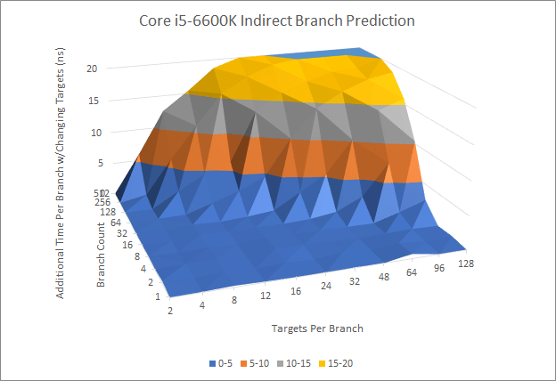
Indirect Branch Prediction
Indirect branches are jumps that can go to multiple targets. This adds another dimension to branch prediction, since the predictor has to guess which target it goes to. Phytium performs reasonably well when a single branch goes to 16 different targets. We see up to 256 indirect targets tracked without significant penalty, with 128 branches that each alternate between two targets.


Again, this capability isn’t on the same level as ARM and Intel’s cores. Skylake can track at least 128 targets for a single branch, and at least 1024 total indirect targets (512 branches, 2 targets per branch). For Neoverse N1, we see negligible penalty with a single branch going to 64 targets, and at least 2048 total indirect targets tracked (512 branches, 4 targets per branch).

Call and return pairs are a special case of indirect branches, because return typically go back to where a corresponding call came from. For that reason, CPUs typically predict returns with a special return stack. Like A72, Phytium’s return stack appears to have the same 31 entry capacity as A72, matching Neoverse N1’s. Skylake has a smaller 16 entry return stack, but can fall back on its indirect predictor if faced with deeply nested calls that overflow its return stack.
In summary, FTC663’s branch predictor is quite terrible. Skylake’s predictor, which itself looks barely changed from 2013-era Haswell’s predictor, outclasses it in every metric. Back in the Skylake days, ARM had a pretty mediocre predictor in their Cortex A72. But ARM has come a long way since then, and Neoverse N1 enjoys a fast, accurate predictor that also beats the stuffing out of Phytium’s. I was also going to talk about the predictors in AMD and Intel’s latest architectures, but on second thought, doing so in this Phytium article would be downright mean.
Frontend: Code Fetch Bandwidth
Next, let’s look at how fast Phytium’s frontend can bring instructions into the core – that is, as long as it’s not being misled or stalled by the branch predictor. FTC663 appears to have a 48 KB L1 instruction cache, just like Cortex A72. The core has a 3-wide decoder, but just like A72, it can only decode one NOP per cycle. A NOP is the simplest instruction you can have (it stands for No OPeration), so this is a bit weird. To get around this, we’re using a modified version of our instruction bandwidth test for A72 and FTC663 that uses a mix of NOP and mov x0, 0.

FTC663 and A72 both take a sharp drop in instruction throughput when fetching code from L2, although FTC663 does somewhat better. Interestingly, the Phytium core maintains almost exactly 1 IPC when running code out of L2. If Phytium uses a predecode scheme like A72, maybe the predecode mechanism can only process one instruction per cycle.
Neoverse N1 and Skylake both enjoy superior instruction-side bandwidth throughout their cache hierarchy. N1 can feed its core from L2 almost as fast as Phytium can from its L1i. And Skylake can sustain higher instruction bandwidth from its L3. ARM and Intel’s modern-ish architectures also enjoy higher cache capacity. Combined with their decoupled BTBs, N1 and Skylake can expect to maintain decently high IPC even as code spills out of their instruction caches. In contrast, FTC663 will struggle to feed itself in such a situation.
Rename/Allocate Stage Optimizations
A lot of modern CPUs can optimize certain instructions as they’re being sent to the execution engine, allowing it to extract more IPC or reduce load on execution pipes. FTC663, like Cortex A72, does none of these things. In terms of helping the backend out, it doesn’t do anything more than the basic register renaming stuff you can learn in computer science classes.

Neoverse N1 and Skylake in contrast both offer some form of move elimination. They can also eliminate certain operations that would always give a zero result, reducing load on their ALU pipes.
Out of Order Execution Engine
Out of order execution lets a CPU avoid getting stuck on long latency instructions. To do so, the CPU’s backend has queues and buffers that track instructions in various stages of execution before committing the results in-order. FTC663’s execution engine looks like a beefed up version of Cortex A72’s. It has decently sized buffers that are comparable in some areas to Neoverse N1, but generally falls short of Skylake.

Compared to A72, FTC663 has similar reordering capacity for loads, branches, and flag-setting instructions. Both CPUs also use 64-bit FP/vector registers, and allocate multiple of those to deal with 128-bit NEON instructions. Phytium has boosted register file and reorder buffer sizes to give FTC663 a generational boost in reordering capacity over A72. They’ve also increased FTC663’s store queue size to 28 entries, which is quite a boost over A72’s tiny 15 entry one. None of these CPUs can do more than one store per cycle, making the store queue a pretty “hot” structure because it drains slowly. Phytium has made the right move by beefing up this queue.
But a CPU’s backend has to stall the renamer once any micro-op needs an entry from a queue that’s full, so it’s just as important to look at what structures didn’t see a size increase.

Phytium failed to correct a few of A72’s glaring weaknesses. A72’s load queue was already a bit small, only covering 25% of its ROB size. It’s not hard to find applications where more than 25% of instructions read from memory. Phytium didn’t scale the load queue up, meaning that it’ll likely fill and stall rename before the ROB or register files fill. They also didn’t increase the number of renames for the flag register. Finally, FTC663 suffers from the same inefficient vector register allocation issues as A72, meaning that the vector register file fills quickly. Chances are that Phytium will struggle to make use of its increased reordering capacity, as buffers that already had marginal capacity on A72 become even more stretched.
Neoverse N1 and Skylake have a more balanced allocation of OoO resources, with better coverage of ROB capacity for various types of instructions (except scalar FP). Therefore, they’ll achieve better reordering capacity in practice.
More Parallels with A72?
FTC663’s out-of-order engine makes some strange resource allocation decisions that we don’t see very often. But quite often, these characteristics are also found on Cortex A72. To start, the FP register file is large enough to cover the entire reorder buffer. Usually, CPUs have FP register files with comparable entry counts to their integer register files. That’s because all code has to use integer registers to address memory and handle control flow, but not everything uses floating point registers. Also, both A72 and FTC663 are inefficient with their 128-bit register allocation. Each 128-bit result claims more than two 64-bit registers, resulting in slightly low reordering capacity for 128-bit NEON code. A72 and FTC663’s designers may have opted to implement a lot of 64-bit FP registers to cope with this inefficiency in register allocation.
FTC663 and A72 also suffer from strange limits on NOP reordering capacity. NOPs do nothing, so normally you wouldn’t expect them to consume anything more than a reorder buffer entry, and sometimes not even that. That’s why we usually try measuring reorder buffer capacity by seeing how many NOPs we can place between long latency cache misses before the OoO engine can no longer handle both cache misses in parallel. For reasons that I can’t comprehend, A72 and FTC663 can only reorder past 38 NOPs, even though they can reorder past well over 100 FP instructions. Even stranger, NOPs appear to be consuming a shared resource in the OoO engine. If we put 30 NOPs between the cache misses, our reordering capacity with integer registers drops to around 70 (down from 96).
Execution Units
We didn’t dig into detailed instruction throughput and latencies, but FTC663’s execution units appear largely identical to Cortex A72’s. Both feature four specialized ALU pipes. Two handle simple integer operations, one handles branches, and one handles complex integer operations. Execution units are poorly distributed across the pipes, because the complex integer pipe is likely to be under-utilized compared to the others.

I suspect the integer ports are set up that way to simplify result bus scheduling, rather than increase integer throughput. According to Agner Fog, some CPUs could suffer delays when an execution port is handling instructions with different latencies. That’s because the execution port only has one result bus, and can’t handle two instructions trying to write their results back at the same time. On A72 and Phytium, this problem is avoided on the two ALU pipes and branch pipes because just about everything that goes through them will finish in a single cycle. The result bus scheduling problem would then be limited to the “complex” integer pipe.
FTC663 has a pretty weak vector/FP execution side. Vector and FP execution throughput is identical to A72’s for the instruction mixes we tested. Most FP/vector execution units are half width (64-bit), and 128-bit operations are issued twice. Only the integer ALUs have 128-bit width. However, they’re not broken into two micro-ops like on AMD K8, and only occupy a single scheduler slot. Floating point and vector execution latencies are sub-par, considering FTC663’s low clock speed.

N1 also has two FP/vector execution pipes, but features full-width execution units. In most cases, N1 will be able to complete two 128-bit instructions per cycle while FTC663 can only do one.

Finally, Skylake has very strong vector execution thanks to AVX2 support backed by full-width execution units. Intel has been a leader in vector execution performance ever since Sandy Bridge, and Skylake continues that tradition.
Load/Store Execution
Like A72, FTC663 has two memory pipes – one for loads and one for stores. However, Phytium has implemented a unified AGU scheduler, which should be more efficient than A72’s distributed one. Typical code has far more loads than stores, so A72 will probably see situations where its load AGU scheduler fills up, but entries are available in the store scheduler. FTC663 avoids that, but still has limited memory execution resources, just like A72. Modern high performance cores tend to feature more robust AGU setups. For example, ARM’s Neoverse N1 has two memory pipes capable of handling both loads and stores. Skylake has an even more powerful AGU setup that can sustain two loads and a store every cycle.

Once addresses are generated, they’re passed to the load/store unit (LSU), which ensures correct ordering for memory operations. Unlike newer Intel, AMD, and ARM CPUs, FTC663’s LSU can’t speculate on whether memory operations are dependent. Thus, load operations cannot execute until all prior store addresses are known and can be checked for overlaps. If there is an overlap, the store’s data is “forwarded” to the load. Latency for store forwarding is typically a bit higher than that of uncontested L1D latency, and Phytium is no exception. Store forwarding latency is 7 cycles, and Phytium’s mechanism works for all cases where the store and load overlap. Unlike other CPUs, there’s no expensive fallback path for partial load/store overlaps. The only penalties are an extra three cycles if the load and store partially overlap and both cross a 64 byte cacheline boundary, or an extra two cycles in some partial overlap cases that cross a 16 byte boundary. Neither of these are particularly expensive.


The overall picture’s similar to A72’s, though FTC663 improves by avoiding some penalties when crossing a cacheline boundary. With respect to store forwarding performance, FTC663 and A72 both compare well to Neoverse N1 and Skylake, which suffer high penalties when stores and loads partially overlap.

For independent accesses, there are still a few cases that can reduce L1D throughput on FTC663. Stores cost an extra cycle if they cross a 16 byte boundary, and loads cost an extra cycle if they cross a 64 byte cacheline boundary. I suspect the A72 and FTC663’s L1D caches are divided into 16 byte sectors, but loads that cross 16B boundaries don’t suffer a penalty because the cache has two read ports. Compared to Skylake and N1, FTC663 and A72 are more likely to suffer from misaligned store penalties.
Memory Access: Latency
Making a cool looking core is one thing, but feeding it is another. Phytium D2000 has a triple level memory hierarchy. Each core has its own 32 KB L1D. Each cluster of two cores has a 2 MB L2 cache, and the whole chip shares a 4 MB L3. L1D latency is four cycles, like Skylake and many other CPUs. But with FTC663’s low clock speed, a 3 cycle L1D would have been nice to see.
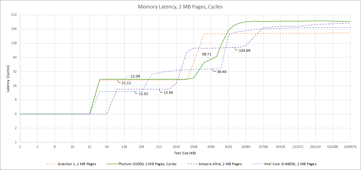
Latency degrades quickly as we move down the cache hierarchy. FTC663’s shared L2 cache has reasonable capacity, but takes 22 cycles to access, giving it almost the same actual latency as Skylake’s much larger L3. When we get to L3, latency is horrible at somewhere over 50 cycles. Actual latency is over 20 ns, which is similar to Cascade Lake’s L3 latency and not a good showing for a client platform. At least some form of L3 is better than nothing at all.

Finally, memory latency is a disaster at 164 ns. Phytium D2000 ends up suffering higher memory latency than the two server chips in this comparison. To show just how bad it is, a dual socket Xeon X5650 system can access remote memory with just over 120 ns of latency. That’s right: Westmere is accessing DDR3 memory attached to another socket, and still getting to it faster.
Memory Latency with 4K Pages
Testing memory latency with 2 MB pages helps isolate cache performance, but most client workloads use 4 KB pages. With 4 KB pages, TLB capacity and performance is far more important. FTC663 and A72 both appear to have a 32 entry L1 DTLB, but both see a strange increase in latency within L1D capacity with 4 KB pages. From above, this penalty goes away when 2 MB pages are used, so it’s definitely some kind of TLB miss penalty.

The L2 TLB on A72 and FTC663 adds about 7 cycles of latency over a L1 TLB hit, and seems to have a capacity of around 1024 entries.
Memory Access: Bandwidth
Like with A72, cache bandwidth on FTC663 is generally poor. Vector performance wasn’t a high priority for the core anyway, so we weren’t expecting to see high cache bandwidth. Still, the single load AGU could be a handicap even in scalar integer workloads. Cores with more than one load AGU seem to issue two load operations for a significant number of cycles.

Skylake is designed to be a heavy hitter in vector workloads, so it features massive cache bandwidth. N1 has lower cache bandwidth, since it emphasizes power and area efficiency over vector performance. Still, N1 is miles ahead of FTC663 and A72, showing how far ARM has come since the A72 days.
When we hit all threads in the chip, Phytium’s D2000 closes the gap because we’re letting it bring eight cores to bear against four Skylake or Neoverse N1 cores. But it only closes the gap a little bit.

Compared to Graviton 1, Phytium’s D2000 sees improved L2 performance because each L2 cache instance only has to service two cores. Looking closer at Graviton 1, Phytium may have chosen to implement dual core clusters instead of quad core ones because L2 cache bandwidth couldn’t scale to fully feed four cores. Graviton 1’s L2 bandwidth stops scaling past two threads:

Phytium may be stuck with a similar L2 design, and opted to implement more L2 instances to avoid L2 bandwidth bottlenecks. ARM and Intel both field more advanced shared cache implementations, which use mesh or ring interconnects. Cache slices are distributed across mesh or ring stops, and allow better bandwidth scaling for multithreaded workloads.
Topology, and Core to Core Latency
As mentioned before, Phytium’s D2000 uses dual core clusters. Cache coherency operations are relatively fast within a cluster, but are much slower when cluster boundaries have to be crossed.

Amazon’s Graviton 1 sees similar latencies, but uses quad core clusters.
Although core to core latency will have minimal to no effect on most applications, Intel is able to achieve far better latency in an octa-core design by using a ring bus.

AMD also arranges cores into clusters, but achieves far better latency both within and across clusters.
Conclusion (for normal consumers)
Phytium’s D2000 targets desktop, mobile, and embedded markets. Maybe it’s adequate for embedded uses, but the D2000 is completely uncompetitive on desktop and mobile. It gets clobbered in well threaded loads by Intel’s i5-6600K, which has fewer cores and hit the market more than seven years ago. AMD and Intel’s current offerings can beat the i5-6600K without breaking a sweat, so you can imagine how far behind Phytium is.
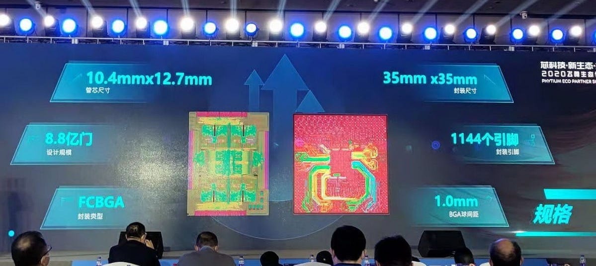
Price doesn’t help Phytium either. We paid over $500 for the D2000 system. For the same price, we could have built an octa-core Zen 3 based PC. Given that option, there’s zero reason for any consumer to consider the D2000. Even if the D2000 got a massive price drop, it’s hard to imagine where it could make sense. The i5-6600K sells for about $50 on the used market, which doesn’t leave Phytium’s D2000 with much room to undercut it. In fact, Phytium probably can’t undercut the i5 without selling chips at a loss. HKEPC posted Phytium slides showing 132.08 mm2 die area, which is larger than Skylake’s 122.4 mm2 die.
If you wanted to know whether Phytium’s D2000 is a good CPU choice for your next desktop or laptop, you can stop reading now, because it’s definitely not.
Conclusion (with political context):
Phytium is not a startup trying to compete with established players. Instead, it’s a company that works with China’s military, and is almost certainly supported by government funding in an effort to build up indigenous chip making capability. The exact details are beyond the scope of this article, but to put it simply, China is in the awkward position of continuously pissing off its Asian neighbors – neighbors that happen to be technological giants responsible for producing a large part of the world’s supply of high performance microprocessors. On top of that, those Asian powers (South Korea, Japan, Taiwan) have close relations with the US, which is also not amused when China shoots a ballistic missile over one of them. Like other developed societies, China is very dependent on high performance microprocessors for day to day function. Given this situation, China has put a lot of focus into domestic microprocessor design, and Phytium’s D2000 is a product of this. We should therefore evaluate D2000 from the perspective of how it helps China build self reliance, from both a short term and long term view.
In the short term, I don’t think D2000 helps China. Its performance is extremely uncompetitive even against desktop chips from a decade ago, to the point that China would be better off dumpster diving for old Intel and AMD chips. Personally I’d hate to be stuck using a D2000 even for everyday web browsing, let alone more demanding use cases like photo and video editing. Grabbing old desktop chips off the used market would cost less while providing a more usable computing experience, and give China better resistance against possible sanctions.
The other angle is that China’s making a long term investment into chip production, and D2000 represents an early effort. D2000 is not expected to be cost efficient, because chip manufacturing is extremely complex and has high entry costs. Instead, China’s paying well above market price for products like the D2000 in order to build domestic expertise and manufacturing capability. So let’s ignore cost and performance competitiveness for the moment, and look at what FTC663 shows about China’s progress in domestic chip design. Several factors make me very unenthusiastic about China’s efforts going forward.
To start, I don’t think FTC663 is a ground up indigenous design. FTC663 is similar to A72 in far too many places, including quirks that we’ve seen with A72 that aren’t obvious design choices and that don’t show up anywhere else. To list some of them:
Identical instruction throughput and latencies for every mix of instructions we tested. Beyond what we listed before, both have 5 cycle integer multiply latency, and both are similarly inefficient at using both FP/vector pipes when given scalar FP operations.
NOP throughput limited to 1 per cycle, even though the core is 3-wide
NOPs consume OoO resources beyond a ROB entry
Inefficient vector register allocation for 128-bit instructions
48 KB L1 instruction cache (not a common size) with coupled BTB, which maxes out at 4096 branch targets.
Increased L1D latency and lower bandwidth with 4 KB pages when test size exceeds 16 KB (unexplained TLB penalty?)
Add in other similarities like identical L1 and L2 data-side bandwidth, matching load queue sizes, and same number of flag register renames, and there’s way too much to be a simple coincidence. For example, Centaur’s CNS is nominally a Haswell-class core, but the two architectures have massive internal differences. Even different generations of Intel architectures have bigger differences than FTC663 and A72.
If Phytium didn’t develop the architecture from the ground up, we can evaluate their expertise by seeing how they iterated on A72. If they managed to deliver a generational performance leap, or brought advanced microarchitecture features into the core, then we can say China’s starting to build a solid base of knowledge. Unfortunately, Phytium’s changes do not represent a good iteration over A72

Reordering capacity boost will be blunted by lack of size increases for important structures (i.e. the load queue) that were already too small to start with. The increase in L2 code fetch bandwidth seems to be held back by a L2 that’s still very low performance. Branch predictor regressions nerf those improvements. You don’t benefit much from speculating farther ahead or pulling in code faster if you end up throwing out that extra work because of a branch mispredict.
Basically, Phytium takes one step forward and one step back, while retaining all of A72’s fundamental weaknesses – ones that ARM (the company) largely corrected in their subsequent designs. If we look over at Neoverse N1, it’s simply worlds apart from A72. Sure, N1 doesn’t boast higher maximum reordering capacity than FTC663. But N1 has a lot more in common with high performance Intel and AMD desktop chips than it does with its A72 predecessor. It has a very accurate branch predictor, fast branch handling with long-range BPU-driven code prefetch, a low latency L2, can hoist loads ahead of stores with an unknown address, and a balanced allocation of OoO resources that will let it better utilize its theoretical reordering capacity than FTC663. ARM’s engineers didn’t have the area or transistor budget that Intel enjoys with their high performance desktop cores, but they knew how to allocate area/transistors in the places that mattered most. That’s how they put N1 a country mile ahead of FTC663, and that shows ARM has strong engineers.
ARM and Phytium seemed to share a common starting point from the A72. However, ARM has competent engineering teams with a firm grip on the basics of designing high performance architectures, and that gave them the ability to meaningfully iterate on their designs. I can’t say the same for Phytium, and thus I can’t say I’m enthusiastic about their long term prospects. Still, it’s fun to see different designs, and things can always change. We look forward to seeing what Phytium does in the future.
If you like our articles and journalism and you want to support us in our endeavors, then consider heading over to our Patreon, or our PayPal if you want to toss a few bucks our way. If you would like to talk with the Chips and Cheese staff and the people behind the scenes then consider joining our Discord.