
The Weird and Wacky World of VIA Part 2: Zhaoxin’s not quite Electric Boogaloo


In Part 1 of this piece we talked about the third x86 design house, VIA and more specifically VIA’s most recent commercially available architecture Isaiah. Today we are talking about the joint venture that VIA has with the Shanghai Municipal Government, Zhaoxin.
A Little Background History
Zhaoxin was started in 2013 as a joint venture between the Shanghai Government and VIA.
Based on the information on Wikichip, Zhangiang is a minor modification of the Isaiah II core where the biggest changes were the addition of the Chinese hashing algorithms SM3 and SM4 to Padlock.
The big architectural changes came with the Wudaokou core where Zhaoxin claimed a 25% performance per clock increase, which is no small feat. The core we are looking at today is Zhaoxin’s latest, Lujiazui, which Zhaoxin claims has an up to 50% performance increase over Wudaokou however, the clock speed increase is also up to 50% which make me suspect that Lujiazui is the Wudaokou core ported from HLMC’s 28nm to TSMC’s 16nm and has had a nice clock bump as a consequence.
Lujiazui versus Isaiah What has changed?
Cache Money….. Or in this case an exchange
One of the largest changes that Zhaoxin did with the Lujiazui architecture is to the cache hierarchy.
Zhaoxin has cut the L1 in half from Isaiah going from a 64KB L1 to a 32KB L1. This is an interesting move for a few reasons: a smaller L1 is lower power, costs less die area, and will reduce the hitrate of the L1 so more requests go out to the L2.
Speaking of that, Lujiazui’s 4MB L2 is now shared across a quad core cluster, ditching Isaiah’s private 1 MB of L2 per core. Thus Lujiazui has a last level cache configuration similar to that of AMD’s Zen 1 and Zen 2 APUs which is a massive change because Isaiah did not have shared caches.
However, this new shared L2 came at a large cost. L2 latency went from 20 cycles on Isaiah to an astonishing 48 cycles on Lujiazui. For comparison, Zen 1’s L3 (LLC) is twice as big at 8MB but has 35 cycle latency even though Zen 1 runs at a higher clock.
This would suggest to us that this is not designed to be a high performance design, however both Zhaoxin and VIA claim that the KX-6000 series is designed to go up against Skylake in performance which is a high performance core. Now, Tom’s Hardware did a very in-depth performance review of the KX-U6780A and found that it in no way matches up to Skylake for performance.
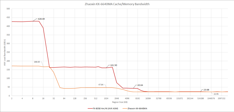
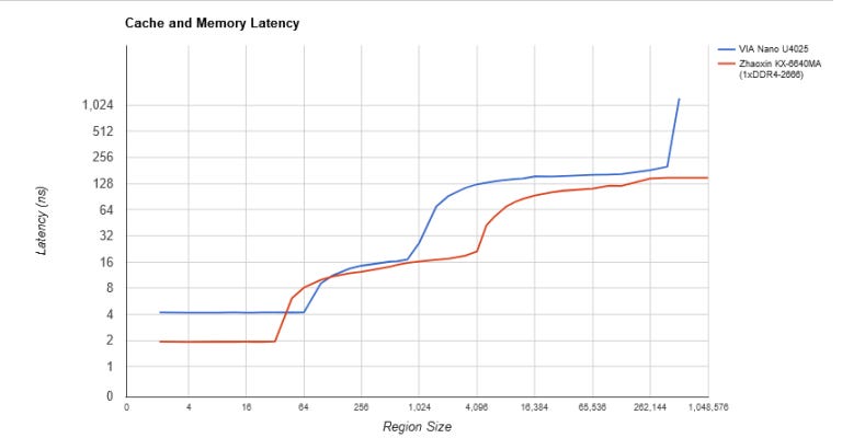
Lujiazui’s cache bandwidth is unimpressive even when compared to other CPUs that don’t use a full-width AVX implementation (more on that later). We weren’t even able to sustain 8 bytes per cycle to each core from the L2 cache. Single threaded bandwidth, shown below, is also nothing to write home about. Clearly, the cache hierarchy will need to be improved if Zhaoxin really does want to go up against Zen 2.
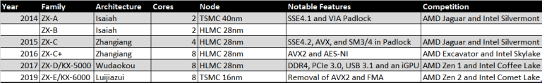
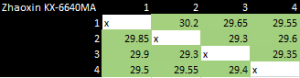
Beyond the L2, Lujiazui brings the memory controller on-die instead of accessing it through a Front-Side Bus (FSB), reducing memory latency and Lujiazui’s intra-cluster interconnect gives reasonably low latencies when bouncing cache lines between cores:
The All-Important Branch Predictor Unit
In the previous part of this article we talked a lot about Isaiah’s very unique BPU and how it seemed to trade off speed for accuracy.
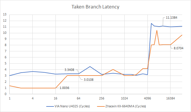
Zhaoxin tries to get the best of both worlds by adding a 16 entry L0 BTB that can handle taken branches with no bubbles. Zen 2 has a similar mechanism, and can typically handle about half of the branches it sees without going to larger, higher latency BTBs. Lujiazui’s main BTB, like Isaiah’s, has 4096 entries and creates two bubbles if it’s used to provide a branch target. If there’s a BTB miss, Lujiazui is able to provide a branch target slightly faster than Isaiah.
Now let’s look at how well the branch predictor can handle long, repeating patterns.
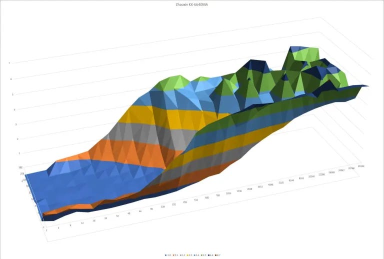
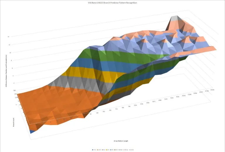
Pattern recognition capabilities haven’t changed much. As you can see, the VIA and the Zhaoxin BPUs are very similar in this test. Isaiah’s direction predictor was very sophisticated for a low power core in 2008. But a decade later, it’s rather mediocre. High performance cores available when Lujiazui launched, like AMD’s Zen and Intel’s Skylake, can handle much longer patterns without mispredicts:
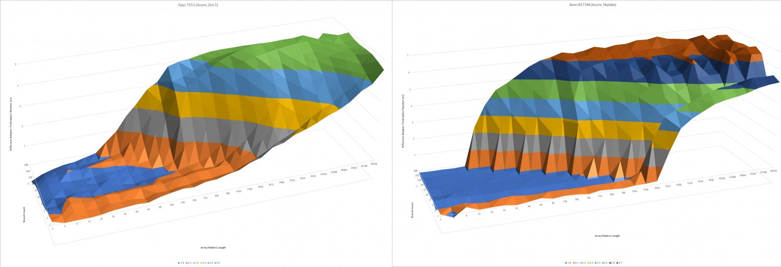
ARM’s Cortex A75 is a contemporary architecture with a more comparable direction predictor. A75 a low power core designed for use in smartphones, so this is another sign that Lujiazui isn’t really designed to go head to head with Intel and AMD’s best.

Lujiazui’s call/return prediction is peculiar:
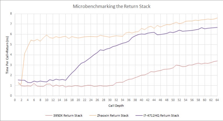
It looks like Lujiazui implements a fast but tiny L1 return stack with only two entries. Lujiazui probably has a L2 return stack with 34 entries, as performance counters only show mispredicts after call depth exceeds that.
5-6 nanoseconds is 13 to 16 cycles at 2.6 GHz, so this L2 return stack is horrendously slow. Hitting Lijiazui’s L2 return stack is about as bad as overflowing the return stack on Haswell. Deeply nested calls should be avoided on Lujiazui, even if they’re correctly predicted.
A Smaller, Narrower Core?
This came as a bit of a surprise to us but it looks like Lujiazui has narrowed the decode width from 3-wide in Isaiah to 2-wide. Rename and/or retirement appear to be 2-wide as well – a test where half the instructions decode into two micro-ops only runs at 1.5 IPC, or 2 micro-ops per cycle.
The three reasons as to why you would choose to narrow the core are if you want higher clock speed, lower power, and/or a smaller area that your core takes up. However, the reason that Zhaoxin was going purely for higher clock speed doesn’t hold up because Isaiah hit the same clock speed as Wudaokou with both architectures maxing out at 2GHz on a 28nm process.
Zhaoxin probably cut width down in order to build an 8-core chip with acceptable power and die area. This is a good reminder that a wider core running at lower clocks isn’t always better. ARM’s A73 also decreased core width to 2-wide (from 3-wide on the A72) to improve power efficiency, so Zhaoxin’s move is not without precedent.
The ROB and Register Files – Going Backwards?
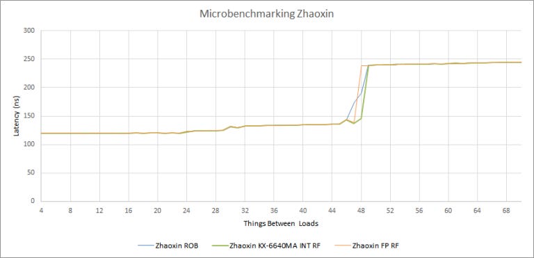
Zhaoxin also cut the ROB (reorder buffer) size from 65 to 48 entries. We’re limited by Lujiazui’s 48 entry ROB even if we use instructions that write to integer or floating point registers, indicating that there are enough register file entries for every instruction in the ROB. Apparently, Lujiazui ditched Isaiah’s separate register files and went back to a P6-style ROB+RRF. Pretty much all modern high performance CPUs use register files decoupled from the ROB, so this is a puzzling choice.
One guess is that a ROB+RRF scheme requires less storage for registers, because integer and FP/SIMD instructions share the same register file. It’s probably simpler to implement too, because you only have to deal with the ROB regardless of whether an instruction writes to a register.

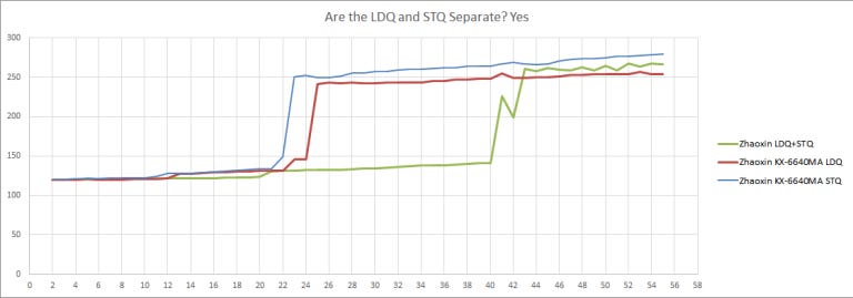
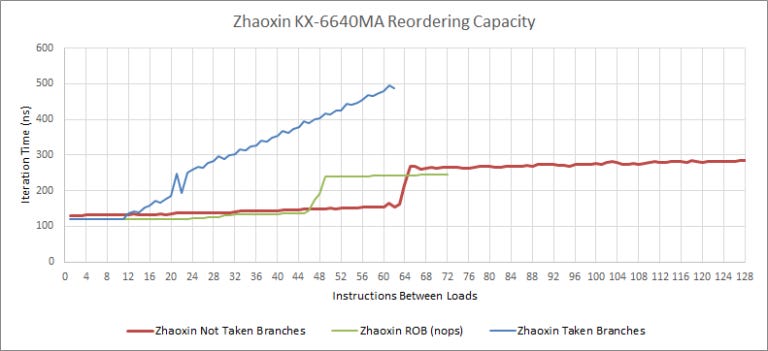
To their credit, Zhaoxin has implemented an interesting optimization for not-taken branches to soften the blow of a smaller ROB. Specifically, we were able to get two long latency loads to execute in parallel with up to 64 not-taken branches between them. Each of these branches is a cmp + je pair, so that’s 128 instructions in flight. Not-taken branches account for around 5 or 7% of the instruction stream (in Cinebench R20 and Call of Duty Vanguard respectively). So, Lujiazui’s effective reordering capacity may not be as far behind Nano’s as the ROB size suggests. We couldn’t find any other instruction or combination of instructions that could get past a limit of 48 in flight.
Scheduling All These Trains
Ok the CPU isn’t actually scheduling trains, it’s just my really bad attempt to say that we are now looking at Lujiazui’s schedulers.
Zhaoxin seems to have largely kept Nano’s port layout while rebalancing scheduler sizes to improve performance with common integer workloads. The integer scheduling queues grew by a little bit, and we see one more scheduler entry available for the ALUs compared to Nano.
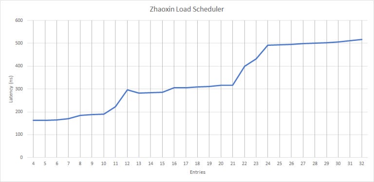
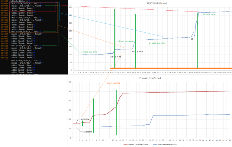
On the memory side, Lujiazui increases the load scheduler size to 12 entries, and similarly beefs up the store scheduler to 20 entries. Compared to Isaiah the store scheduler has increased by 4 entries and the load scheduler has increased by approximately 7 entries.
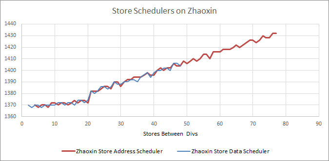
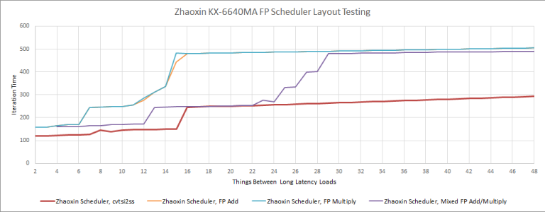
Lujiazui has rebalanced and slightly cut down the FP/SIMD side schedulers. The FP multiply and add ports have 12 entry scheduling queues, unlike Nano’s 8+24 split.
Execution Ports
We’re assuming Lujiazui keeps most of Nano’s port layout and execution units. Because the core is 2-wide, it’s very difficult to determine which execution units are on separate ports. When possible, we tried to see which instructions could start executing together. If that technique is impossible (for example if one instruction can go to two ports, making core width a limitation rather than execution ports), we tried to see whether they shared a scheduling queue.
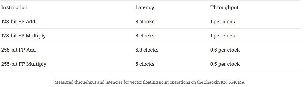
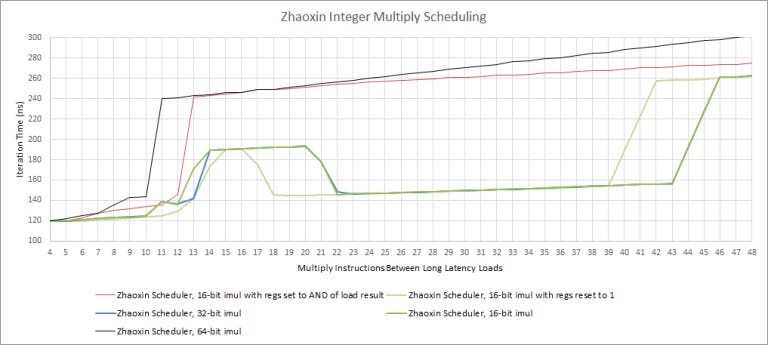
Like Isaiah/Nano, Lujiazui has two ALU ports and handles integer multiplication differently based on register width. For example, IMUL with 16-bit inputs has a latency of 2 cycles. With 64-bit multiplication, latency goes up to 9 cycles. They also go to different scheduling queues. Floating point throughput has not changed.
Zhaoxin has beefed up the execution engine in some areas too. There are now two 128-bit vector integer ALUs, instead of one in Isaiah. Lujaizui also gets an extra load pipe, letting it sustain two 128-bit loads per cycle from the L1 data cache.
On the other hand, Lujiazui loses Isaiah’s impressive 2-cycle floating point adder. FP addition latency is now 3 cycles.
AVX – Supported on Paper, Not Useful in Practice
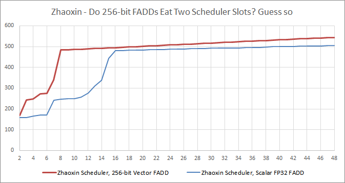
Tomshardware described Lujiazui’s AVX performance as “subpar“, and we can easily see why. 256-bit AVX instructions are split into two 128-bit micro-ops and thus consume two scheduler entries. Since the core seems to be two micro-ops wide, using AVX instructions doesn’t provide a throughput advantage over SSE.
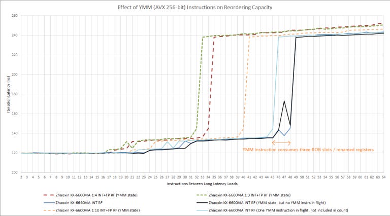
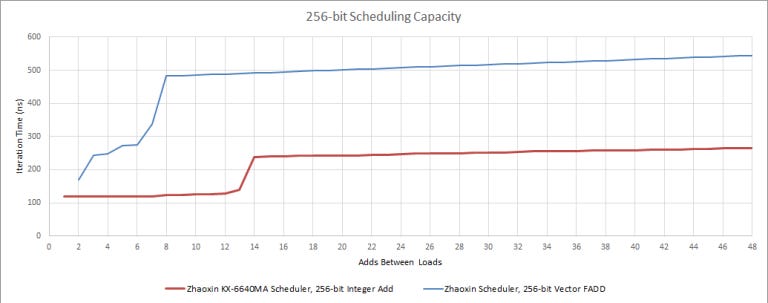
But things get worse. Reordering capacity drops to less than half for 256-bit instructions:
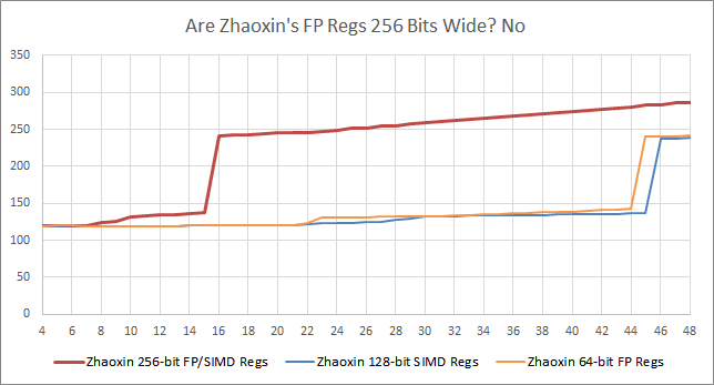
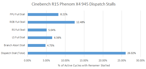
It seems like 256-bit AVX instructions consume more than two ROB slots. That’s a worrying penalty in a core with an already small ROB. To put things in perspective, AMD’s K10 architecture featured a 72 entry ROB, and suffered heavily from the ROB filling up:
256-bit ops are further penalized by increased latency on Lujiazui:
Zhaoxin’s AVX implementation on Lujiazui looks like a minimum effort job done only to ensure compatibility with newer software. Piledriver and Zen 1 also split 256-bit AVX instructions into two 128-bit micro-ops, but keep latency the same. And, they don’t suffer penalties beyond what you’d expect from an instruction that decodes into two micro-ops. It’s totally fine to use 256-bit AVX instructions on those two AMD architectures. You won’t get an increase in reordering capacity or math throughput, but you still get better code density.
On the other hand, 256-bit AVX should be avoided on Lujiazui. Any instruction density advantage is outweighed by a wombo combo of increased execution latency and reduced reordering capacity.
Loading Loading Loading, Storing Storing Storing
Isaiah’s had fairly small load and store queues with both being 16 entires a piece. Lujiazui has increased both the load and store queues to 24 and 22 entries respectively, delivering a generational improvement.
Like Isaiah, Lujiazui seems to lack memory dependence prediction. Loads can’t be reordered ahead of stores with an unknown address. This was a shiny new feature when it debuted in Core 2, but just about every high performance core can do it today.
And now to put it ALL Together
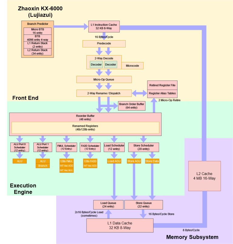
With all the data we have gathered, we have been able to create an approximate block diagram of Lujiazui.
In Conclusion
Wudaokou and Lujiazui are very much not just a reskinned Isaiah. It’s a significantly different design that trims and rebalances VIA’s original Nano design, letting it reach higher clock speeds with a moderate IPC increase.
But Lujiazui is definitely a low power core without high performance aspirations. A lot of changes seem to target die area and power efficiency rather than performance. A 25% IPC gain over a decade is nowhere near enough to catch AMD or Intel. In terms of per-core performance, contemporary high performance Intel and AMD CPUs completely sweep Lujiazui away.
In some ways, Lujiazui is Nano in reverse. Nano was a low power core on paper, but its architecture was beefier than low power cores that launched years later, and wasn’t far off contemporary high performance designs. Meanwhile, Lujiazui aims to compete with Intel and AMD’s big cores, but is nowhere near that. AMD’s Jaguar and Intel’s Goldmont would probably be better points for comparison.
Now this article has gotten very long so the benchmarks of the Zhaoxin versus the Nano will have to wait for a Part 3 but I will say that Zhaoxin’s claim of 25 percent more performance per clock isn’t just hot air.
If you like what we do and you would like to help us with acquiring more things to test, then head on over to our Patreon if you want to chip in a few bucks.
Appendix
P6-Style ROB and Register Files
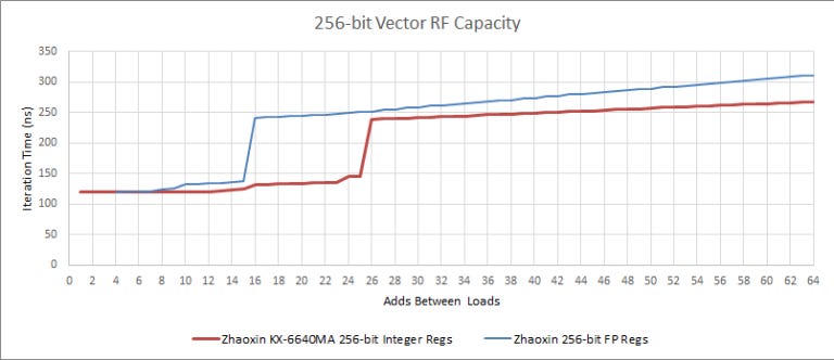
When mixing integer and 256-bit AVX instructions, we see one renamed register file used for both. With separate integer and FP register files, mixing integer and FP register file usage will increase your register-limited reordering capacity to the sum of both (which generally means ROB capacity becomes the limit). But with Lujiazui, mixing in 256-bit AVX instructions reduces reordering capacity, so integer and vector instructions are competitively sharing one one register file.
And as we mentioned earlier, 256-bit AVX instructions seem to consume more than two ROB slots/renamed registers. If we have one 256-bit AVX instruction blocked from retiring by a long latency load, we can only get 45 integer adds in flight before a second load is blocked from entering the backend.
Even if there are no 256-bit AVX instructions pending retirement, simply having 256-bit values present in the YMM registers influences Lujiazui’s ROB/RF entry reclamation logic. As you can see from the black line, having YMM state introduces a spike shortly before we get to 48. That result was repeatable, and isn’t noise.
We were surprised to see a newer CPU with less reordering capacity, so we tried a batch of other things to see if we could get long latency loads to execute in parallel with more than 48 instructions between them.
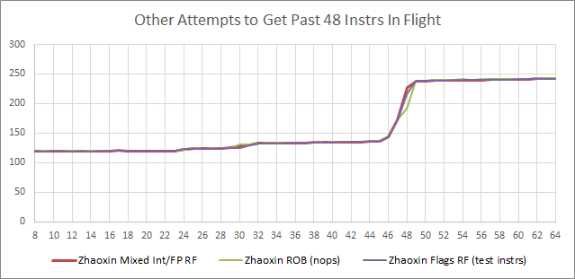
Of those attempts, only one using not-taken branches was successful (as noted earlier). Also, Zhaoxin can have about 20 taken branches pending retirement before the backend has to stall the frontend.
Integer Multiplication
Lujiazui also has incredibly weird behavior with 32-bit and 16-bit multiplies. Reordering capacity varies depending on the values being multiplied, so the CPU might be able to eliminate multiplies (like when an input is 1) when the scheduler is full.
Partial AVX2 Support
Officially, Lujiazui supports AVX, but not AVX2. AVX2 includes FMA (fused multiply add) and 256-bit integer instructions. As expected, FMA instructions generate a fault. However, 256-bit integer instructions appear to work correctly. Just like with AVX/FP, 256-bit integer instructions are decoded into two 128-bit micro-ops. Funny enough, 256-bit packed integer multiplication doesn’t suffer additional latency compared to 128-bit ops.

Also, 256-bit integer addition doesn’t reduce reordering capacity as severely 256-bit floating point ops do. This is pretty strange – Zen 1 gives identical results regardless of whether the 256-bit registers are being accessed by integer or floating point instructions.
Because Lujiazui has two 128-bit integer ports, each with its own scheduling queue, 256-bit integer operations end up getting more scheduling capacity too.
It looks like Zhaoxin has actually done a decent job with 256-bit integer operations, but couldn’t expose them because they don’t support other parts of AVX2 (namely, FMA).
Interpreting FP Scheduler Results
If you’re particularly eagle-eyed, you might have noticed that our FP scheduler graphs have multiple latency jumps. That’s because creating a dependency for a floating point instruction isn’t 100% straightfoward. Integer dependencies are easy – just have test instructions consume the result from the long latency loads used to block retirement.
One way ot create the dependency for FP instructions is to convert the integer load result to floating point (cvtsi2ss). But the cvtsi2ss instruction itself could consume a floating point scheduler slot. So for the most part, we used the result from a long latency load to index into a separate array of floating point values. For those tests, we’re looking at the final jump in latency, because that shows when only one load is executing in parallel.
Here’s a visual explanation, with the test loop unrolled (as it would be in the CPU’s backend)
Assume the first two pointer chasing loads have completed. That is, the loads that put results into registers edi and esi. Loads marked with green lines are ones that are ready to execute.
The first, lowest latency stretch is when the CPU is only limited by memory latency and available instruction level parallelism. Then, iteration latency increases as the CPU’s out of order engine is able to see fewer loads (because the FP scheduler is filling up, preventing it from accepting more instructions).