
Gracemont: Revenge of the Atom Cores

This article can be considered a part 2 to our Golden Cove article because today we are looking at the other core in Alder Lake, Gracemont. Which is in my opinion more interesting than Golden Cove because, spoiler alert, it’s not a little core in the slightest.
Gracemont is a 5-wide out-of-order architecture that traces its roots to 2013’s Silvermont and if we stretch even further back, Intel’s in-order Atom cores can be considered distant relatives too. Compared to Intel’s big core line, which evolved from Sandy Bridge (2010) and is a distant relative of P6 (1995), the Atom line is much younger and has seen sweeping changes from one generation to the next.
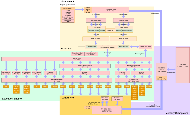
Block Diagram: Atom Goes Wide and Deep
Here’s a high level view of Gracemont, the new addition to Intel’s Atom line and it looks nothing like early Atoms, and it is basically a high performance core.
Branch Prediction: Definitely “Core Class”
Gracemont may be a smaller core than Golden Cove, but still does out of order execution with a large reordering window. Therefore, branch prediction remains extremely important for it’d be a pity if Gracemont queued up a couple hundred instructions in the reorder buffer only to throw them out because of a mispredicted branch so accurate branch prediction helps efficiency by reducing wasted work.
Intel’s Architecture Day 2021 presentation stated that Gracemont’s predictor has “deep branch history and large structure sizes” with a 5K entry branch target cache (also called a BTB, or branch target buffer). Tremont, Gracemont’s direct ancestor, had what Intel claimed was “Core class branch prediction” so let’s have a look at those claims.
Pattern Recognition (Direction Prediction)
Gracemont’s direction predictor looks surprisingly similar to Golden Cove’s, except for a gentle increase in time per branch after the pattern length exceeds 1K which points to an overriding predictor, like the one in Zen 2. Intel probably had to make a tradeoff between predictor speed and power and as a result Golden Cove prioritized speed, while Gracemont takes a more balanced approach. Still, Gracemont’s predictor is better than Skylake’s, so “Core class branch prediction” and “deep branch history” are both accurate descriptions.
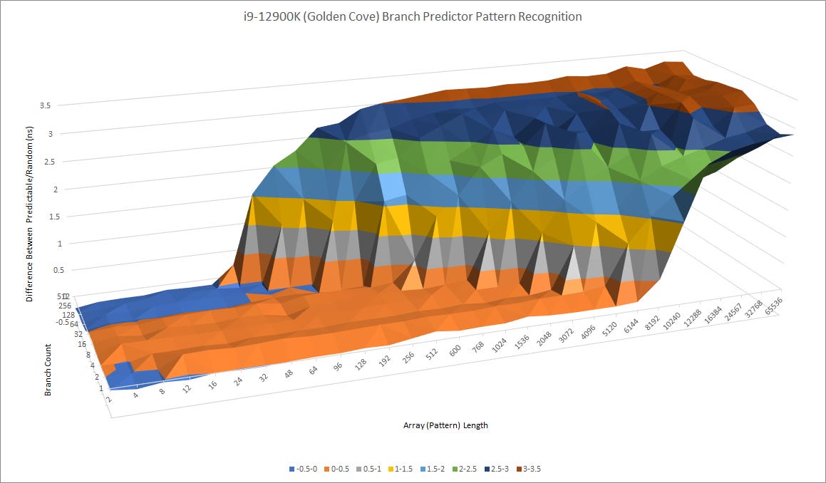

Compared to Zen 2, Gracemont can track similar history lengths. The first level predictor on Gracemont is significantly more capable, meaning Gracemont will suffer fewer frontend bubbles for branches that require longer history length to accurately predict but Zen 2 still has an advantage once more branches come into play.


Finally, we’ll compare Gracemont to ARM’s Cortex A78. Alder Lake is the first desktop chip to use hybrid cores so unfortunately there’s no direct desktop comparison but, A78 has seen use in high end SoCs as a mid-core that balances performance with power efficiency and Gracemont fills the same role in Alder Lake.
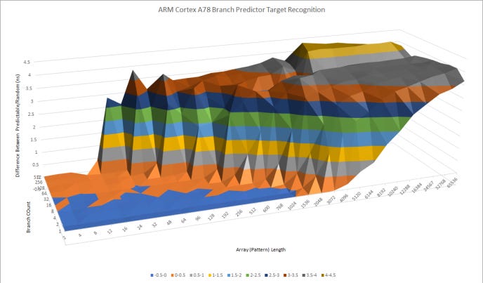

ARM uses a non-overriding predictor that can deal with relatively long history lengths, but stops short of Gracemont’s capabilities and A78 particularly struggles when the branch count hits 512.
Branch Target Tracking (BTB)
Gracemont’s 5K entry BTB may seem small next to Golden Cove’s jaw dropping 12K branch target cache but Golden Cove is an exception. 5K entries is right in line with Sunny Cove and Zen 3’s BTBs, while being larger than the 4K BTBs in Skylake and before. And size isn’t everything – speed matters too.
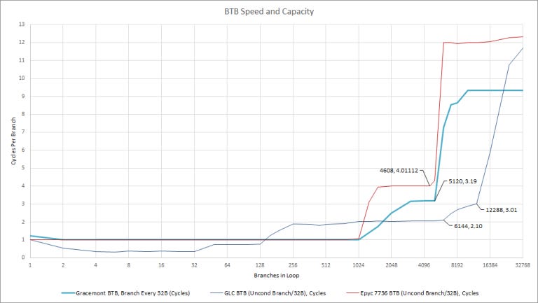
Like Zen 3, Gracemont can do zero bubble predictions with up to 1024 branches however unlike Zen 3, Gracemont’s L2 BTB adds two cycles of latency instead of three. Looking at latencies in absolute time gives a clearer picture of what’s going on.
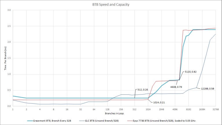
Zen 3 and Golden Cove are both optimized for maximum performance, running at high clock speed to reduce the absolute-time latency for most operations. However, reducing latency in some areas is much harder, the L2 BTB is great example of this, and AMD chose to add an extra pipeline stage instead of paying the power and area cost of making it faster.
Meanwhile, Gracemont has more moderate performance aims and runs below 4 GHz. But lower clocks don’t mean everything gets slower and Intel was able to use fewer pipeline stages for L2 BTB access, resulting in similar absolute-time latency. Finally, Golden Cove goes all out for speed, keeping L3 BTB latency at 3 cycles even at over 5 GHz.
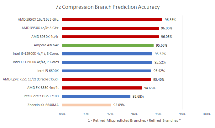
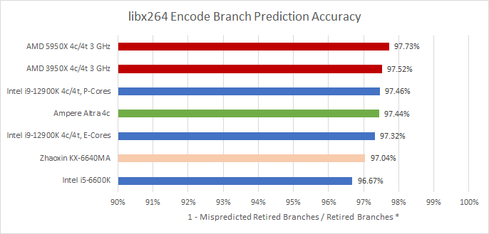
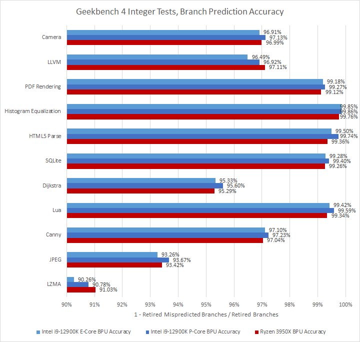
Prediction Accuracy in Practice
Intel loses in compression workloads and libx264, but the situation is a lot more complicated with Geekbench 4 integer subtests where Intel has an advantage there, with Gracemont landing some wins over Zen 2’s predictor. In any case, Gracemont’s ability to land in the same ballpark as high performance cores is impressive.
Instruction Fetch and Decode
Instead of using a micro-op cache, Gracemont uses dual decode clusters, each fed by a 16 byte/cycle port from the instruction cache:
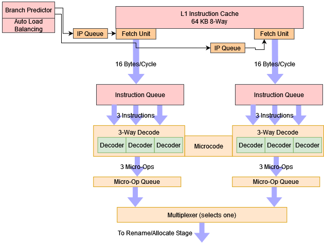
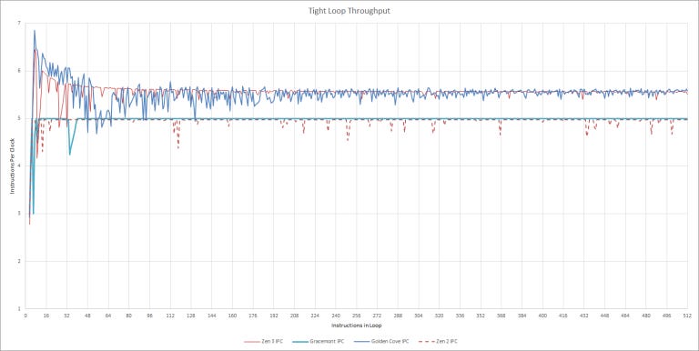
This scheme appeared with Tremont, where it could only switch decoders at taken branch boundarie and Gracemont improves load balancing between the two decode clusters by automatically switching, instead of relying on taken branches. That helps performance in very long unrolled loops, which could get stuck on one decode cluster on Tremont. When we tested with longer loop lengths, we didn’t see any drop off in Gracemont’s instruction throughput:
To programs, Gracemont’s decoder should function just like a traditional 6-wide decoder, fed by a 32 byte/cycle fetch port which goes both ways and compared to old school linear decoders, a clustered out-of-order decoder should lose less throughput around taken branches. Sadly, it looks like Gracemont’s renamer can only feed from one cluster’s micro-op queue at a time so in very small loops, Gracemont suffers the same throughput drop as other cores.
With even larger loop sizes, we can see that Gracemont sustains 32 bytes/cycle fetch bandwidth all the way until L1i capacity is exceeded. In the L2 region, we see about 16 bytes per cycle – in line with other CPUs. As code spills out into L3, throughput takes a sharp drop.
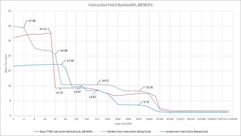
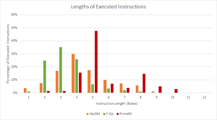
Without a micro-op cache, Gracemont is less suited to AVX workloads, which tend to have longer instruction lengths, but this shouldn’t be a huge issue for Gracemont, because its AVX throughput is not particularly high (as we’ll see later). The results above with 8 byte NOPs are more representative of an extreme AVX workload:
If we use 4 byte NOPs, we can see instruction throughput without fetch bandwidth limitations:

With more common instruction lengths, Gracemont maintains a steady 5 instructions per cycle throughout the entire 64 KB L1 instruction cache. For test sizes between 32 KB and 64 KB, it even beats Golden Cove and Zen 3. This larger L1i a welcome improvement over the 32 KB designs we’ve seen in recent x86 big cores. This is partly because Gracemont can’t afford to miss L1i as often. Its L2 is slower and higher latency, while the smaller BTB makes instruction prefetching less effective.
Still, I’d like to see large instruction caches return to high performance x86 cores. More L1i hits mean higher and more consistent instruction throughput. Intel also says a larger L1i is more power efficient, which makes sense because a lot of CPU power is used simply moving data around:
Even cores that target high performance have to balance that with power efficiency which means that moving fewer bytes around is a good way to get more efficiency, so it’s weird that AMD ditched Zen 1’s 64 KB L1i in favor of using one that’s half the size on Zen 2.
Rename/Allocate – Getting Ready to Find Parallelism
The rename/allocate stage is responsible for allocating resources in the CPU’s out-of-order execution engine. It’s often called the renamer, because it renames architectural registers to physical ones. However, “Renamers” in today’s CPUs have evolved a bit compared to their ancestors a few decades ago and can pull a few more tricks to enable more parallelism.

Move elimination is one such trick, and a natural extension of register renaming. Instead of telling the backend to copy values between registers, the renamer can simply point two architectural registers to the same physical one which means register to register move instructions don’t use any ALU ports, and more importantly, never consume scheduler slots while appearing to execute with zero latency. Gracemont has Zen 2 like move elimination abilities, which is quite powerful and a huge step up from Intel’s older big cores. It’s also a massive improvement over previous Atom line architectures.
Another trick is recognizing special cases of independence. If a program sets a register to zero, for example by XOR-ing it with itself, obviously you don’t need to wait until you know the register’s previous value before generating the result. Gracemont can recognize these cases, but doesn’t completely eliminate them like Golden Cove or Zen 3. They still seem to consume an ALU port, since throughput is limited to 4 per cycle.
Gracemont’s rename/allocate stage isn’t a match for Golden Cove’s, which can eliminate just about everything under the sun and then some. But Gracemont is a massive improvement over cores from the Atom line. According to Agner, with Goldmont (Gracemont’s grandfather) “no more than one move can be eliminated per clock cycle” and “move elimination often fails”, however compared to older big cores like Skylake and Haswell, Gracemont still has a better rename stage.
Gracemont’s Out-of-Order Engine
To absorb latency and extract parallelism from a single thread, Gracemont has rather large buffers, especially for a core that doesn’t target maximum performance. Again, we’ll refer anyone who needs an explanation to Travis Down’s blog, and jump straight into Intel’s strategy with Gracemont.
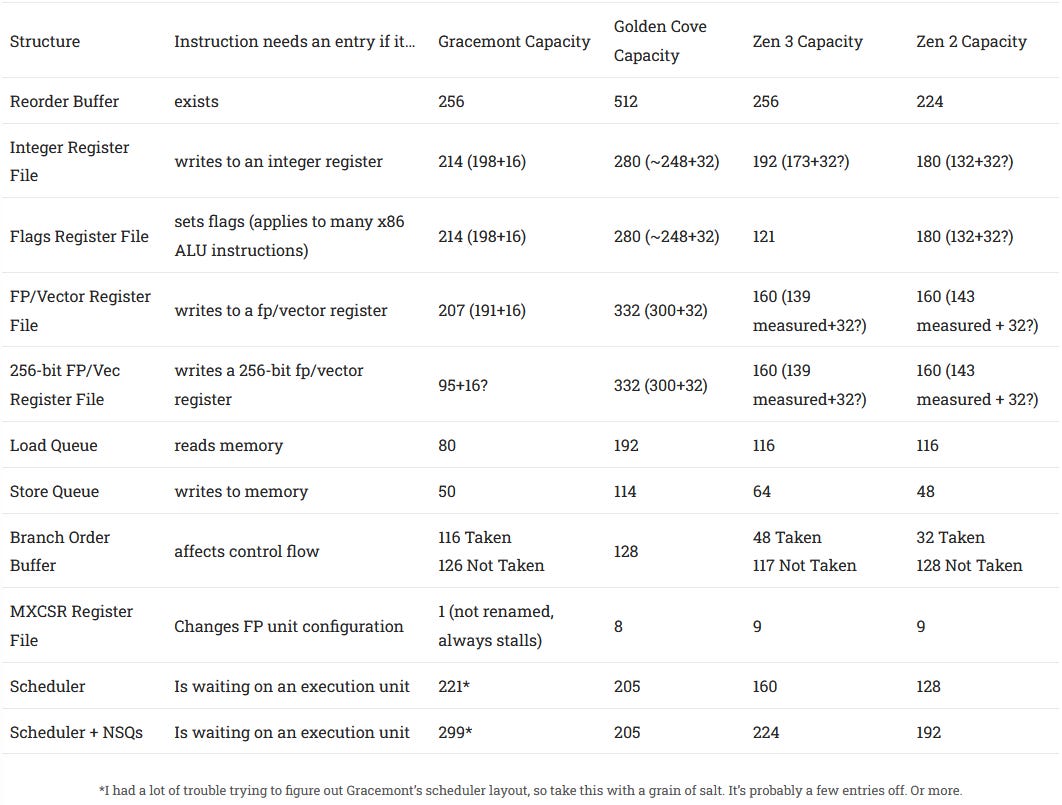
With a few exceptions, Gracemont’s ILP extracting resources are comparable to those of Zen 2 and Zen 3. Still, some Atom DNA shines through and the floating point unit’s configuration register (MXCSR) is not renamed at all, along with any writes to it will bring out-of-order execution to a grinding halt. Efficiency is in focus too so to reduce register file size, 256-bit instructions are split into two 128-bit micro-ops much like Zen 1, and corresponding vector registers are also 128-bits wide. The 207 entry vector register file would thus be 3.3 KB in size, compared to at least 10 KB on Golden Cove and 5 KB on Zen 2/3. Gracemont thus avoids implementing a large vector register file, while maintaining plenty of renaming capacity for scalar floating point and 128-bit vector loads. Even for applications that take advantage of AVX2, Gracemont looks fine:

With 256-bit writes in the mix, libx264 on average will consume 47 Gracemont vector registers per 100 instructions. So Gracemont still has plenty of vector register file capacity for workloads like video encoding. Only extreme cases like Y-Cruncher (where over 70% of executed instructions write 256-bit results) will put pressure on Gracemont’s FP/vector renaming capacity.
On the integer side, Gracemont has impressive resources. 77% of in-flight instructions can write to integer registers – a ratio that compares favorably to that of recent big cores from Intel/AMD. Reordering capacity for branches is insane. Almost half of the instruction stream can be taken branches. If there’s anything we can find fault with, it’s the load and store queues. They’re a touch small and may have a harder time absorbing bursty memory activity, particularly if accesses miss the L1 or L2 caches and maximum reordering capacity is needed.
Scheduling and Execution Units
Integer Side
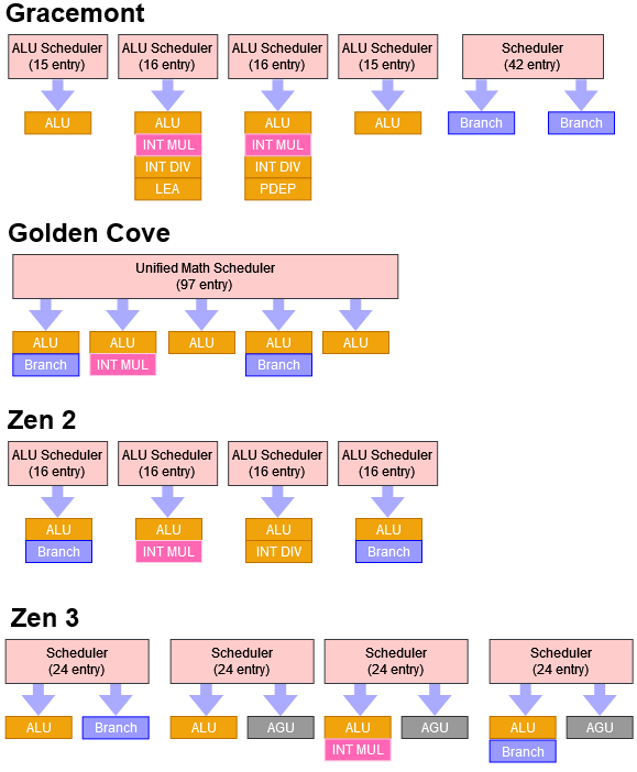
Intel’s P6 line has been defined by unified schedulers with lots of ports ever since the architecture debuted in 1995. In contrast, the Atom line uses distributed schedulers. Much like previous Atom CPUs and AMD’s CPUs (as well as many ARM designs), Gracemont uses distributed integer schedulers:
As we mentioned before, a distributed scheme lacks the on-demand flexibility of a unified one, and requires careful tuning to prevent individual queues from filling up. However, unified schedulers are more expensive in terms of complexity, area, and power:
…circuits for unified schedulers are slower than distributed, as each execution unit’s selection logic must search the entire pool of waiting instructions rather than just the scheduler attached to its own execution unit.
Wong, H. T. (2017). A Superscalar Out-of-Order x86 Soft Processor for FPGA [PhD thesis, University of Toronto] Retrieved from A Superscalar Out-of-Order x86 Soft Processor for FPGA | TSpace Repository (utoronto.ca)
One highlight of Gracemont’s implementation is ample scheduling capacity for branch instructions. ALU+Branch ports tend to see higher load and scheduling queues in front of them tend to fill more, so Intel’s choice makes sense.
In terms of scalar integer throughput, Gracemont comes with four ALU ports. That’s plenty for practically all applications but fewer ports can handle certain operations, compared to big cores with 4 ALUs. For example, LEA with a base and scaled offset can only go to one port, while Skylake has two ports available for that. Also unlike big cores, Gracemont has two multipliers however, in exchange the latency is higher at 5 cycles, compared to 3 cycles on both Golden Cove and Zen 3.
Floating Point and Vector Side
Gracemont’s floating point side uses a semi-unified setup. Unlike Golden Cove’s penta-ported, 97 entry monstrosity, Gracemont uses two smaller queues. One triple ported queue handles math operations, while a separate dual ported one deals with vector stores.
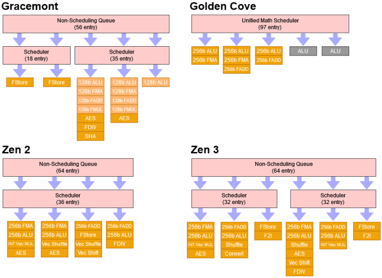
To make up for smaller schedulers, Gracemont takes a leaf out of AMD’s book and uses a big non-scheduling queue (NSQ). As we noted before, this clever approach avoids stalling the rename stage when the FP scheduler fills, while being cheaper than a bigger scheduler. With this layout, Gracemont’s backend have up to 91 vector/FP operations waiting to execute before stalling the renamer. That should be plenty for scalar FP and 128-bit vector code, and approaches big core queue capacity. That capacity is also necessary with AVX code, since 256-bit instructions consumes two scheduler slots.
Gracemont gets a port configuration similar to that of Intel big cores – just with 128-bit wide units instead of 256-bit ones. Common operations have at least two ports, meaning 256-bit instructions on Gracemont generally don’t incur a latency penalty and have a throughput of at least 1 per cycle. To summarize key execution latencies:

FP/vector execution latencies are not bad, though generally worse than that of the latest big cores. On the bright side, Gracemont drops the high latency vector integer multiplier from Intel’s big cores and all in all, Gracemont has one of the strongest 128-bit FP/vector units in any x86 CPU. It should be a decent (but not outstanding) performer even in AVX workloads.
Address Generation and L1D Access
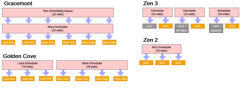
Gracemont can handle two loads and two stores per cycle. That matches Sunny Cove’s load/store throughput except for 256-bit accesses, which count as two on Gracemont. To sustain two stores per cycle, Gracemont relies on combining writes to the same cache line. If a series of stores all go to different 64-byte cache lines, throughput will be one store per cycle, even for scalar 64-bit stores.
Just like the FP side, Intel put a NSQ in front of the store scheduler. Counting this, Gracemont can have 84 memory operations waiting for address generation. That’s more than Zen 3. Even if we count scheduling capacity alone, 62 memory operations is nothing to sneeze at.
Overall, Gracemont has execution throughput and capacity that looks more like a high performance desktop core than an old Atom.
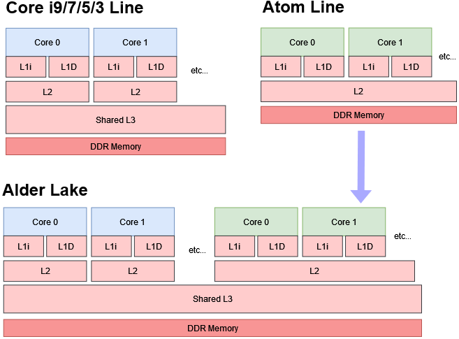
Memory Subsystem: Atom gets a L3
From Nehalem’s debut in 2008, Intel’s big core caching strategy has been defined by a modestly sized L2, or middle level cache. This L2 serves as a buffer between small but fast L1 caches and a large but relatively slow L3. Meanwhile, the Atom line uses a simpler cache hierarchy. A shared L2 is the last level cache, with no middle level.
Gracemont keeps its Atom DNA with a large 2 MB, 17 cycle L2 shared between four cores. On desktop, it gains Alder Lake’s L3, making its memory hierarchy look just like an Atom cluster with a desktop L3:
Latency
As for latency, we’re basically looking at Atom with a L3:
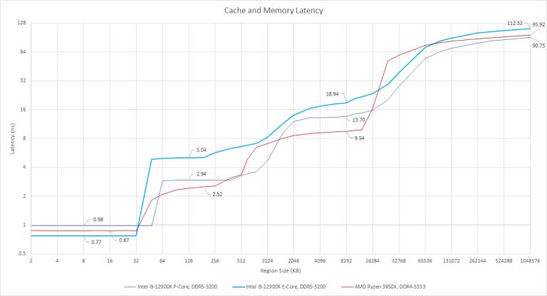
Starting off, Gracemont features a fast, 3 cycle L1 data cache. Despite lower clocks, it can return data faster than Golden Cove’s 5 cycle L1D. A couple cycles and less than a quarter of a nanosecond might not seem like much. But the vast majority of memory accesses will hit L1D, so its low latency is definitely a highlight of Gracemont’s cache hierarchy.
Beyond L1, latencies deteriorate quickly. Up to 2 MB, we see Gracemont’s shared L2 trading speed for capacity. Once we hit L3, we see the same high latency L3 that Golden Cove had to cope with. Even though latency is higher in absolute terms, cycle counts are similar.

For perspective, let’s apply Little’s Law (queue length = arrival rate * latency) again to look at latency while taking reordering capacity into account:

Gracemont doesn’t have enough reordering capacity to absorb L3 latency so catching memory accesses at L2 will be crucial for performance; thankfully, 2 MB should be plenty. For example:
Address Translation
In modern CPUs, where modern means 80386 or newer, programs don’t directly address physical memory. Instead, they access virtual memory addresses, which CPU hardware automatically translates to physical memory locations. This lets the operating system do all kinds of cool things like prevent one buggy program from taking others down, or automatically swapping to disk when physical memory is exhausted. To speed up this address translation, CPUs cache virtual to physical address mappings in TLBs, or translation lookaside buffers.
On the data side, Gracemont has a fully associative, 48 entry L1 TLB. After that, there’s a 2048 entry 4-way L2 TLB. While the L1 TLB is a little small, the L2 TLB impressively matches that of big cores, just with less associativity. But it’s not free:
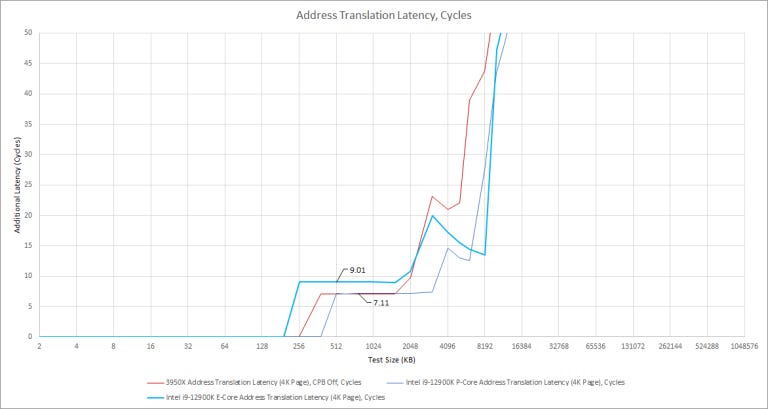
Compared to Golden Cove and AMD’s Zen 2, Gracemont suffers two extra cycles of latency when accessing the L2 TLB. This is likely a power optimization. Gracemont’s setup is likely preferable to a smaller, faster TLB. A L2 TLB miss and page walk could cause up to four additional memory accesses, or five if Sunny Cove’s larger address space is carried over to Alder Lake. Reducing page walks is definitely a good idea for both performance and power.
Bandwidth
Cache and memory bandwidth can be important for vectorized, throughput bound workloads. Gracemont’s unique position makes finding a suitable comparison complicated. Let’s start with performance oriented cores:
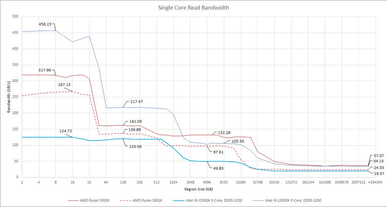
To nobody’s surprise, Gracemont gets smacked around by high-clocking cores with 256-bit data paths. The only bright spot is its L2 cache. The 64B/cycle L2 interface can dynamically give more bandwidth to a single core, resulting in decent per-core bandwidth. Past L2, Gracemont seems limited by high latency. L3 bandwidth is nothing to write home about. And funny enough, DRAM bandwidth is higher with DDR4 than DDR5, because of high DDR5 latency. This suggests Gracemont has conservative prefetchers that aim to save power by not transferring data unless absolutely necessary, at the expense of bandwidth.
Perhaps cores with 128-bit data paths would be a better comparison:
Within this cohort of chips, Gracemont compares favorably. Like Zen 1, L2 bandwidth is almost a match for L1’s. However, L3 bandwidth is still low compared to Zen 1’s.
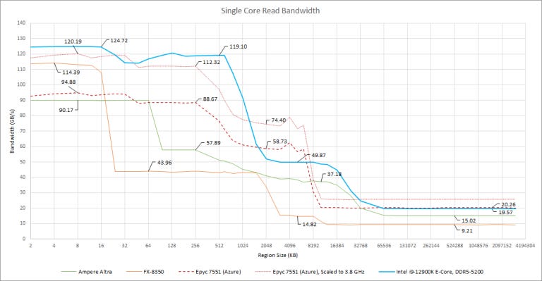
Single core bandwidth is nice for analyzing architecture, but is rather unimportant for performance. If an application is throughput bound and nicely vectorized, it’s likely multithreaded too. Let’s have a look at how bandwidth scales across a Gracemont cluster:
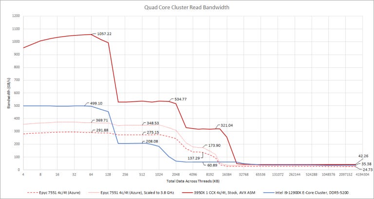
From this test, we see that Gracemont’s L2 interface is shared between all four cores in the cluster. Thus, L2 bandwidth drops to just under 16 bytes per core cycle in this test, handing a win to Zen 1. To illustrate this:
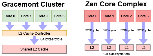
This can be seen as another design tradeoff – a shared cache is more area efficient because read-only data like code and constants don’t have to be duplicated across multiple L2s. In exchange, L2 bandwidth doesn’t scale as well when thread count increases. But this is a good tradeoff. Gracemont’s L2 bandwidth should be adequate for everything except very demanding AVX workloads that miss L1D a lot.
In L3, bandwidth scaling is poor. While the shared ring stop is a possible culprit, a single Golden Cove core can pull around 100 GB/s from L3. More likely, poor bandwidth is a result of Alder Lake’s ring clocking down when Gracemont cores are active, combined with prefetchers tuned for power saving rather than maximum performance.
Finally, let’s hit all eight Gracemont cores in the i9-12900K:
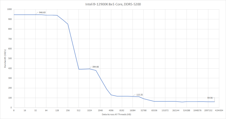
At last, we’re getting good memory bandwidth and seeing DDR5 benefits. L1 bandwidth approaches that of four Zen 2 cores. L2 bandwidth is adequate but unimpressive, due to its shared-per-four-cores interface. L3 bandwidth remains frustratingly poor, and could be a bottleneck even with Gracemont’s moderate vector capabilities.
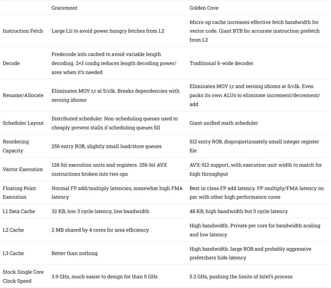
Gracemont and Golden Cove: Different Design Targets
Intel’s Architecture Day 2021 presentation described Golden Cove as a “Performance x86 Core Architecture” and Gracemont as an “Efficient x86 Core Architecture”. Various sites looked straight past the marketing talk and labeled Alder Lake a “big.little” design, drawing parallels with cell phone chips that use tiny in-order cores to handle background tasks but for Alder Lake, Intel’s marketing terms are very accurate.
Unlike Cortex-A55 little cores in cell phones, Gracemont is firmly in high performance territory. It’s a wide core with deep reordering capacity and clock speeds not far off desktop cores from a few years ago. But unlike recent Intel desktop cores, Gracemont makes careful sacrifices to maximize performance per watt and area. To condense differences between the two approaches:
Power Draw
To see what Intel achieved with their hybrid design, we read RAPL (Running Average Power Limit) counters for core and package power during a libx264 4K encode. Core affinity was used to control which cores, and how many cores the encode job was allowed to use. We only took power draw at a specific section of the encode, around frames 90-120 so this test wouldn’t take forever to complete.
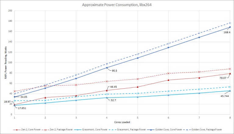
Gracemont draws a surprising amount of power when just one core is loaded. That suggests shared components like the L2 and ring stop draw a lot of power. Gracemont’s efficiency really starts to show as more cores get loaded. With eight cores, we’re seeing 5.72 watts per Gracemont core, compared to 21.05 watts for Golden Cove.
Intel also brackets AMD’s Zen 2 in terms of performance and power consumption. IPC over the entire workload was 1.72, 1.91, and 2.25 for Gracemont, Zen 2, and Golden Cove respectively. Thus Golden Cove is faster, but at a disproportionate power cost. Gracemont does the opposite. It’s slower, but delivers more instruction throughput per watt.
Conclusion
Gracemont is a well balanced core with ample execution resources and reordering capacity. It doesn’t have any serious weaknesses beyond obvious tradeoffs that were made to keep power draw down, but even these sacrifices are well thought out and shouldn’t impact common integer loads. Just to summarize:
Gracemont’s strengths:
Well balanced out of order execution resources
Excellent branching performance (high reordering capacity, large zero bubble BTB, good prediction capabilities)
Large 64 KB L1 instruction cache
Low latency L1 data cache
Modest power consumption
Weaknesses:
L3 access suffers from high latency and low bandwidth
Lower vector throughput than other desktop x86 cores
Ten years ago, Intel used a single architecture to dominate laptops, desktops, servers, and high performance compute. Today, the market is far tougher. AMD’s single threaded performance is extremely competitive, putting Intel’s desktop position in danger and in the server market, AMD’s power efficiency and density threatens to unseat Intel. ARM-based vendors smell blood too and recently gained a foothold by narrowly optimizing for density and power efficiency.
Intel’s position is therefore a bit like that of the Roman Empire in 300 AD. The chip giant still demands respect, with lots of resources and engineering muscle. But it’s facing threats from all directions and in order to maintain its empire, Intel has chosen to abandon the one size fits all approach with its big cores. Instead, the Core line is being unleashed to maximize performance per core while power consumption takes a back seat. Meanwhile, the Atom line abandons Silvermont’s cell phone ambitions to target higher power and performance points, with a focus on density and efficiency.
That brings us to Gracemont; in Alder Lake, we know very well that Gracemont is meant to handle background tasks and boost all-thread throughput. But we can see it hitting other targets too, tablets and fanless ultrabooks come to mind, since Golden Cove won’t be able to stretch its legs in very tight power envelopes. Servers are another target where Neoverse N1 has carved a niche for itself and Intel have definitely taken notice. AMD’s Bergamo will similarly focus on density, bringing 128 Zen 4 cores into a single socket but with its small core area, modest power consumption, and solid performance, Gracemont could be Intel’s ticket into the hyperscale server market as well.
If you like our articles and journalism and you want to support us in our endeavors then consider heading over to our Patreon or our PayPal if you want to toss a few bucks our way.
Appendix
Gracemont’s Integer Scheduler Layout
We’re not completely sure about Gracemont’s integer scheduler configuration, mostly because we can’t find operations that only go to one port for each of the four ALU ports. There are 62 entries available to add operations, though the scheduler obviously isn’t unified. Multiply operations have two ports and 32 entries available. LEA and PDEP both only go to a single port, and each have 16 scheduler entries. Together, LEA and PDEP have 32 entries, indicating they’re on separate scheduling queues. We tried mixing LEA/PDEP with multiply, but based on throughput and scheduling entries available, they seem to share ports.
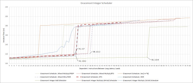
We’re guessing BTS (bit test and set) and ROR (rotate) are on at least one non-multiply port. But we’re not sure which, and can’t determine the size of the last two queues unless we come across some instruction that only executes on one of the remaining ports. I’m sure there’s one, but finding it would probably mean this article never gets finished.
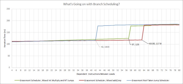
Also, testing showed that Gracemont had 42 scheduler entries available for jumps (both taken and not taken). Mixing jumps and adds gave 63 entries, while mixing jumps and multiplies gave 57:
In the end, we don’t really know what Gracemont’s ALU scheduler looks like. It’s definitely a distributed design, but we can’t determine what queues feed what ports with certainty.
Testing for Non-Scheduling Queues
Gracemont posed a bit of a challenge because some schedulers looked unusually large from naiive testing. If we simply apply Henry Wong’s method for determining instruction window size, and use floating point adds dependent on a pointer chasing load, Gracemont appears to have 91 scheduler entries. Intel already hinted at non-scheduling queues on Tremont, so we suspected they existed on Gracemont too.
To detect them, we use a variation of what Henry Wong described. But instead of varying the number of instructions between pointer chasing loads, we keep that constant. Then, we change how many of them are dependent. Basically this:
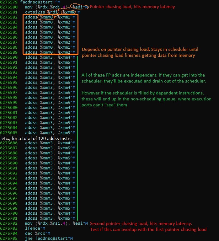
Putting that together with the basic test, we can see Gracemont’s true scheduler size:
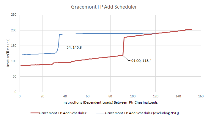
For our approach to work, the total instruction count between the pointer chasing loads has to be greater than the scheduling queue + non scheduling queue size, to ensure we stall the renamer once the scheduler fills. However, it also needs to be less than any limit on the number of instructions pending retirement. In this FP addition example, that means greater than 91, but less than 191.
Revisions
12-23 – updated diagram after further testing, which indicates the load scheduler is not separate from the store scheduler. When testing the load scheduler with dependent loads between long latency ones, the scheduler appeared to have 40 entries, with no evidence of a non-scheduling queue. It also appeared separate from the store scheduler:
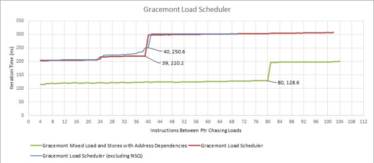
However, doing the same with chained integer divisions to block retirement instead of long latency loads shows that the load and store ports share a scheduling queue:
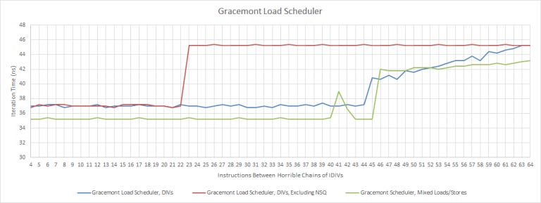
While the two ways of measuring structure sizes usually give similar results on other architectures, this isn’t the case for Gracemont.