
CES 2026: Taking the Lids off AMD's Venice and MI400 SoCs

Hello you fine Internet folks,
Here at CES 2026, AMD showed off their upcoming Venice series of server CPUs and their upcoming MI400 series of datacenter accelerators. AMD has talked about the specifications of both Venice and the MI400 series at their Advancing AI event back in June of 2025, but this is the first time AMD has shown off the silicon for both of product lines.
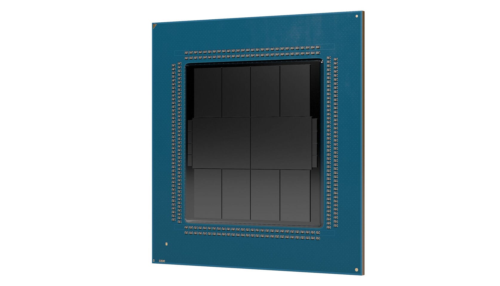
Starting with Venice, the first thing to notice is the packaging of the CCDs to the IO dies is different. Instead of using the organic substrate of the package to run the wires between the CCDs and the IO dies that AMD has used since EPYC Rome, Venice appears to be using a more advanced form of packaging similar to Strix Halo or MI250X. Another change is that Venice appears to have two IO dies instead of the single IO die that the prior EPYC CPUs had.
Venice has 8 CCDs each of which have 32 cores for a total of up to 256 cores per Venice package. Doing some measuring of each of the dies, you get that each CCD is approximately 165mm2 of N2 silicon. If AMD has stuck to 4MB of L3 per core than each of these CCDs have 32 Zen 6 cores and 128MB of L3 cache along with the die to die interface for the CCD <-> IO die communications. At approximately 165mm2 per CCD, that would make a Zen 6 core plus the 4MB of L3 per core about 5mm2 each which is similar to Zen 5’s approximately 5.34mm2 on N3 when counting both the Zen 5 core and 4MB of L3 cache.
Moving to the IO dies, they each appear to be approximately 353mm2 for a total of just over 700mm2 of silicon dedicated for the IO dies. This is a massive increase from the approximately 400mm2 that the prior EPYC CPUs dedicated for their IO dies. The two IO dies appear to be using an advanced packaging of some kind similar to the CCDs. Next to the IO dies appear to be 8 little dies, 4 on each side of the package, which are likely to either be structural silicon or deep trench capacitor dies meant to improve power delivery to the CCDs and IO dies.
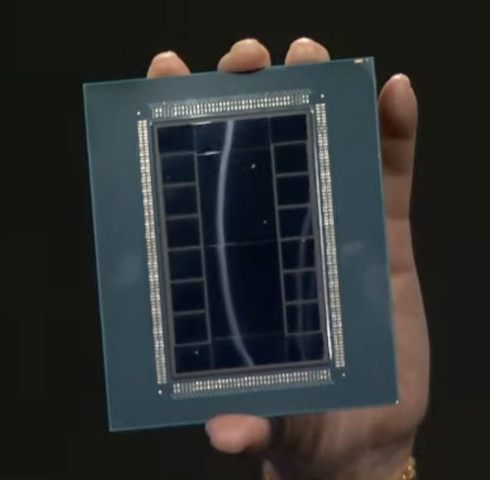
Shifting off of Venice and on to the MI400 accelerator, this is a massive package with 12 HBM4 dies and “twelve 2 nanometer and 3 nanometer compute and IO dies”. It appears as if there are two base dies just like MI350. But unlike MI350, there appears to also be two extra dies on the top and bottom of the base dies. These two extra dies are likely for off-package IO such as PCIe, UALink, etc.
Calculating the die sizes of the base dies and the IO dies, the die size of the base die is approximately 747mm2 for each of the two base dies with the off-package IO dies each being approximately 220mm2. As for the compute dies, while the packaging precludes any visual demarcation of the different compute dies, it is likely that there are 8 compute dies with 4 compute dies on each base die. So while we can’t figure out the exact die size of the compute dies, the maximum size is approximately 180mm2. The compute chiplet is likely in the 140mm2 to 160mm2 region but that is a best guess that will have to wait to be confirmed.
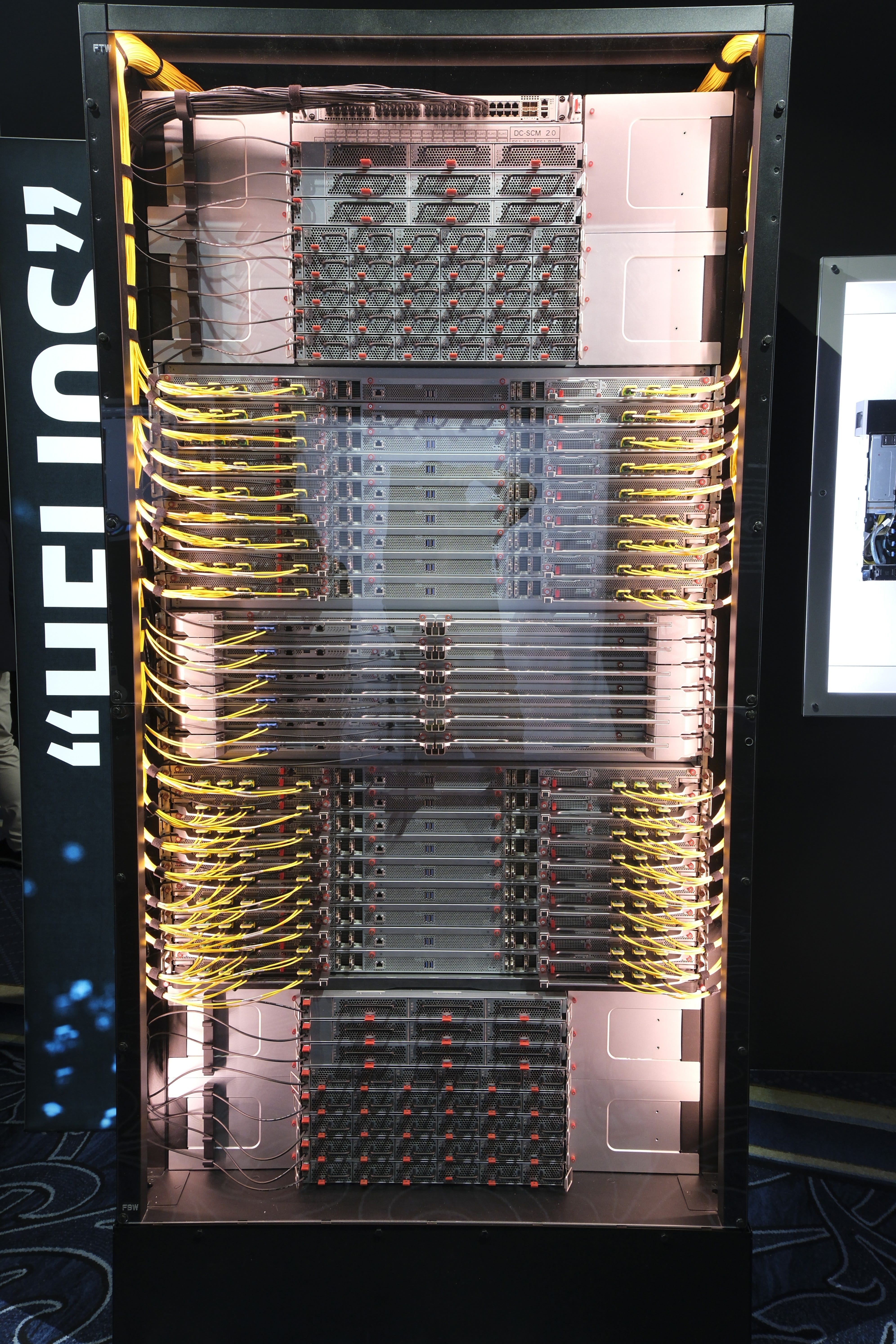
The MI455X and Venice are the two SoCs that are going to be powering AMD’s Helios AI Rack but they aren’t the only new Zen 6 and MI400 series products that AMD announced at CES. AMD announced that there would be a third member of the MI400 family called the MI440X joining the MI430X and MI455X. The MI440X is designed to fit into the 8-way UBB boxes as a direct replacement for the MI300/350 series.
AMD also announced Venice-X which is likely is going to be a V-Cache version of Venice. This is interesting because not only did AMD skip Turin-X but if there is a 256 core version of Venice-X, then this would be the first time that a high core count CCD will have the ability to support a V-Cache die. If AMD sticks to the same ratio of base die cache to V-Cache die cache, then each 32 core CCD would have up to 384MB of L3 cache which equates to 3 Gigabytes of L3 cache across the chip.
Both Venice and the MI400 series are due to launch later this year and I can’t wait to learn more about the underlying architectures of both SoCs.
If you like the content then consider heading over to the Patreon or PayPal if you want to toss a few bucks to Chips and Cheese, also consider joining the Discord.
I believe the CCDs have 48 or 24 corse as amd seems to have associated the cache per CCXs of 12 with 32 cores the CCX configs would be very odd but maybe 4 CCXs of 8 would function ?
They don't seem to be able to connect coherently and with low enough latency 16 cores yet , I mean 12 cores on one CCX is crazy impressive , can't wait to read your article on how they achieved it when Zen 6 comes out !
As the loss of single core performance is not as important for the tasks it's designed for
(Unless I'm making a fool of myself and it's official info and I'm misreading) !
Zen 6c could be minuscule if built on 2nm with the same design changes that compromise frequency for die size , because if MLID is to be believed Zen 6 standard is focused on high frequencies therefore a lot of the die size and transistor budget will go towards achieving that so I'd expect zen 6c to slim down a lot if it let's go of that , also I find odd that they haven't cut the cache in half like on previous dense dies
Hey cheese , thx as always for the informative article , although I have a question , I've read up this previous article of yours to get some reminders about the MII350
https://chipsandcheese.com/p/amds-cdna-4-architecture-announcement
And you seem to mention there it having 4 base dies yet you mention in the current article it having 2 , am I misunderstanding something or is there an error in one of the articles ?
Thx for reading and wish you all the best , and if you have the time , a clarification would be lovely as I can't find any public info on the die config either