
AMD’s RDNA4 GPU Architecture at Hot Chips 2025

RDNA4 is AMD’s latest graphics-focused architecture, and fills out their RX 9000 line of discrete GPUs. AMD noted that creating a good gaming GPU requires understanding both current workloads, as well as taking into account what workloads might look like five years in the future. Thus AMD has been trying to improve efficiency across rasterization, compute, and raytracing. Machine learning has gained importance including in games, so AMD’s new GPU architecture caters to ML workloads as well.
From AMD’s perspective, RDNA4 represents a large efficiency leap in raytracing and machine learning, while also improving on the rasterization front. Improved compression helps keep the graphics architecture fed. Outside of the GPU’s core graphics acceleration responsibility, RDNA4 brings improved media and display capabilities to round out the package.
Media Engine
The Media Engine provides hardware accelerated video encode and decode for a wide range of codecs. High end RDNA4 parts like the RX 9070XT have two media engines. RDNA4’s media engines feature faster decoding speed, helping save power during video playback by racing to idle. For video encoding, AMD targeted better quality in H.264, H.265, and AV1, especially in low latency encoding.
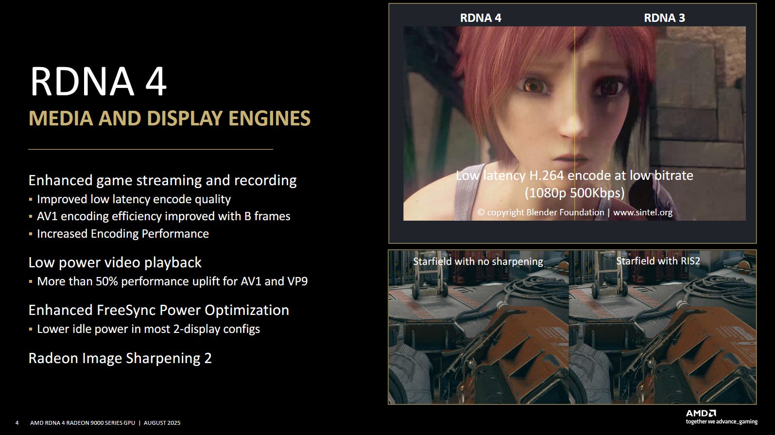
Low latency encoder modes are mostly beneficial for streaming, where delays caused by the media engine ultimately translate to a delayed stream. Reducing latency can make quality optimizations more challenging. Video codecs strive to encode differences between frames to economize storage. Buffering up more frames gives the encoder more opportunities to look for similar content across frames, and lets it allocate more bitrate budget for difficult sequences. But buffering up frames introduces latency. Another challenge is some popular streaming platforms mainly use H.264, an older codec that’s less efficient than AV1. Newer codecs are being tested, so the situation may start to change as the next few decades fly by. But for now, H.264 remains important due to its wide support.
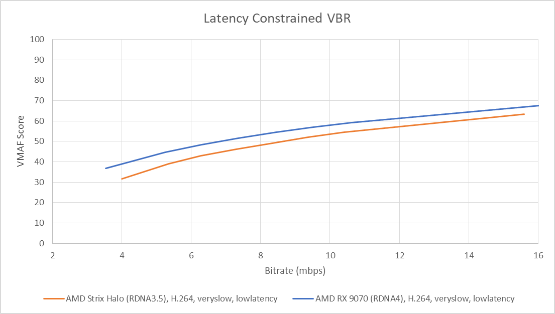
Testing with an old gameplay clip from Elder Scrolls Online shows a clear advantage for RDNA4’s media engine when testing with the latency-constrained VBR mode and encoder tuned for low latency encoding (-usage lowlatency -rc vbr_latency). Netflix’s VMAF video quality metric gives higher scores for RDNA4 throughout the bitrate range. Closer inspection generally agrees with the VMAF metric.
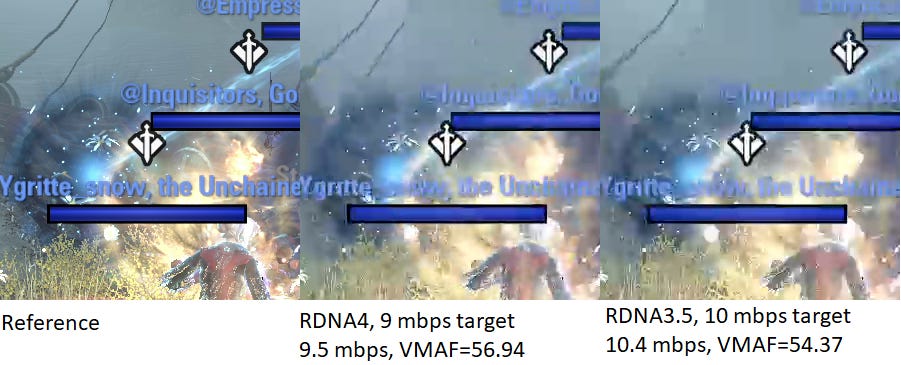
RDNA4 does a better job preserving high contrast outlines. Differences are especially visible around text, which RDNA4 handles better than its predecessor while using a lower bitrate. Neither result looks great with such a close look, with blurred text on both examples and fine detail crushed in video encoding artifacts. But it’s worth remembering that the latency-constrained VBR mode uses a VBV buffer of up to three frames, while higher latency modes can use VBV buffer sizes covering multiple seconds of video. Encoding speed has improved slightly as well, jumping from ~190 to ~200 FPS from RDNA3.5 to RDNA4.
Display Engine
The display engine fetches on-screen frame data from memory, composites it into a final image, and drives it to the display outputs. It’s a basic task that most people take for granted, but the display engine is also a good place to perform various image enhancements. A traditional example is using a lookup table to apply color correction. Enhancements at the display engine are invisible to user software, and are typically carried out in hardware with minimal power cost. On RDNA4, AMD added a “Radeon Image Sharpening” filter, letting the display engine sharpen the final image. Using dedicated hardware at the display engine instead of the GPU’s programmable shaders means that the sharpening filter won’t impact performance and can be carried out with better power efficiency. And, AMD doesn’t need to rely on game developers to implement the effect. Sharpening can even apply to the desktop, though I’m not sure why anyone would want that.
Power consumption is another important optimization area for display engines. Traditionally that’s been more of a concern for mobile products, where maximizing battery life under low load is a top priority. But RDNA4 has taken aim at multi-monitor idle power with its newer display engine. AMD’s presentation stated that they took advantage of variable refresh rates on FreeSync displays. They didn’t go into more detail, but it’s easy to imagine what AMD might be doing. High resolution and high refresh rate displays translate to high pixel rates. That in turn drives higher memory bandwidth demands. Dynamically lowering refresh rates could let RDNA4’s memory subsystem enter a low power state while still meeting refresh deadlines.
I have a RX 9070 hooked up to a Viotek GN24CW 1080P display via HDMI, and a MSI MAG271QX 1440P capable of refresh rates up to 360 Hz. The latter is connected via DisplayPort. The RX 9070 manages to keep memory at idle clocks even at high refresh rate settings. Moving the mouse causes the card to ramp up memory clocks and consume more power, hinting that RDNA4 is lowering refresh rates when screen contents don’t change. Additionally, RDNA4 gets an intermediate GDDR6 power state that lets it handle the 1080P 60 Hz + 1440P 240 Hz combination without going to maximum memory clocks. On RDNA2, it’s more of an all or nothing situation. The older card is more prone to ramping up memory clocks to handle high pixel rates, and power consumption remains high even when screen contents don’t change.
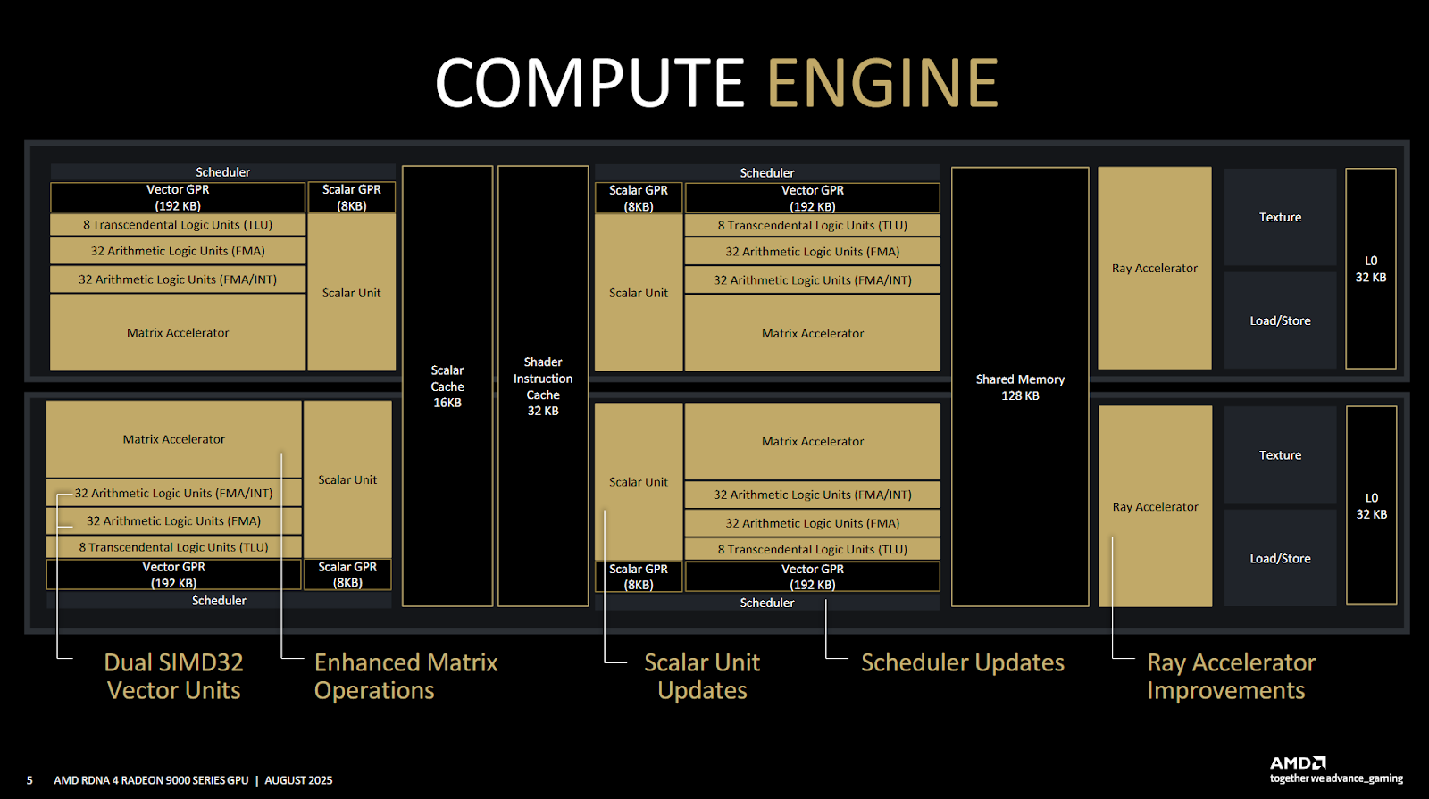
Compute Changes
RDNA4’s Workgroup Processor retains the same high level layout as prior RDNA generations. However, it gets major improvements targeted towards raytracing, like improved raytracing units and wider BVH nodes, a dynamic register allocation mode, and a scheduler that no longer suffers false memory dependencies between waves. I covered those in previous articles. Besides those improvements, AMD’s presentation went over a couple other details worth discussing.
Scalar Floating Point Instructions
AMD has a long history of using a scalar unit to offload operations that are constant across a wave. Scalar offload saves power by avoiding redundant computation, and frees up the vector unit to increase performance in compute-bound sequences. RDNA4’s scalar unit gains a few floating point instructions, expanding scalar offload opportunities. This capability debuted on RDNA3.5, but RDNA4 brings it to discrete GPUs.
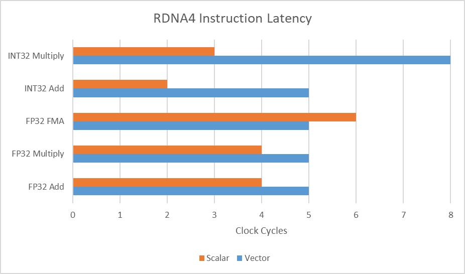
While not discussed in AMD’s presentation, scalar offload can bring additional performance benefits because scalar instructions sometimes have lower latency than their vector counterparts. Most basic vector instructions on RDNA4 have 5 cycle latency. FP32 adds and multiples on the scalar unit have 4 cycle latency. The biggest latency benefits still come from offloading integer operations though.
Split Barriers
GPUs use barriers to synchronize threads and enforce memory ordering. For example, a s_barrier instruction on older AMD GPUs would cause a thread to wait until all of its peers in the workgroup also reached the s_barrier instruction. Barriers degrade performance because any thread that happened to reach the barrier faster would have to stall until its peers catch up.
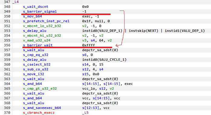
RDNA4 splits the barrier into separate “signal” and “wait” actions. Instead of s_barrier, RDNA4 has s_barrier_signal and s_barrier_wait. A thread can “signal” the barrier once it produces data that other threads might need. It can then do independent work, and only wait on the barrier once it needs to use data produced by other threads. The s_barrier_wait will then stall the thread until all other threads in the workgroup have signalled the barrier.
Memory Subsystem
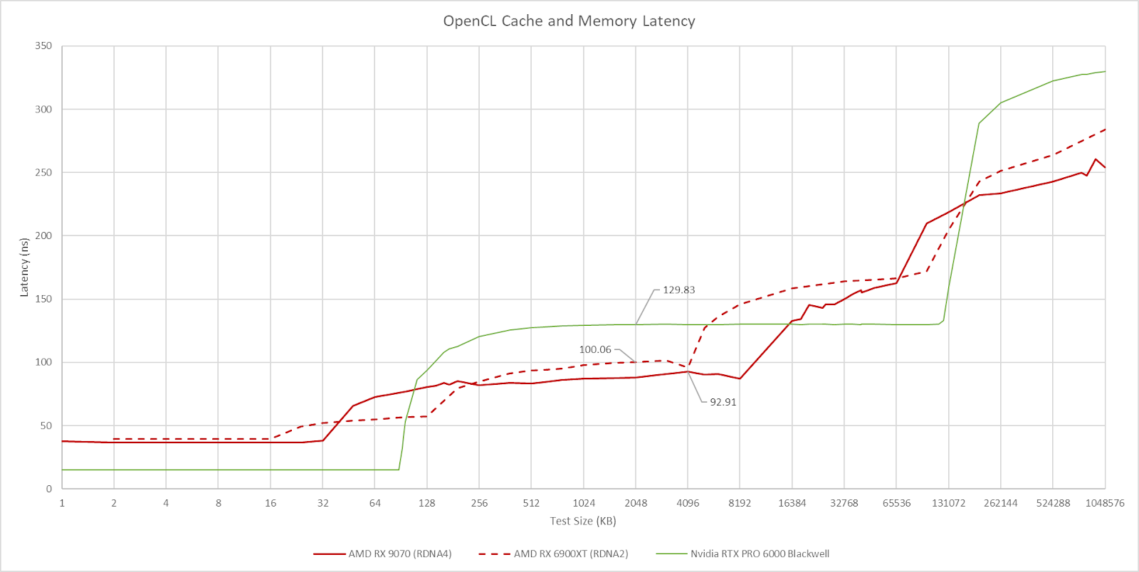
The largest RDNA4 variants have a 8 MB L2 cache, representing a substantial L2 capacity increase compared to prior RDNA generations. RDNA3 and RDNA2 maxed out at 6 MB and 4 MB L2 capacities, respectively. AMD found that difficult workloads like raytracing benefit from the larger L2. Raytracing involves pointer chasing during BVH traversal, and it’s not surprising that it’s more sensitive to accesses getting serviced from the slower Infinity Cache as opposed to L2. In the initial scene in 3DMark’s DXR feature test, run in Explorer Mode, RDNA4 dramatically cuts down the amount of data that has to be fetched from beyond L2.
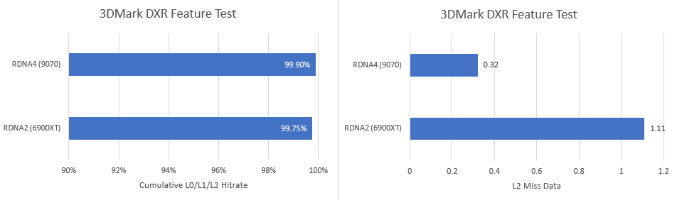
RDNA2 still does a good job of keeping data in L2 in absolute terms. But it’s worth noting that hitting Infinity Cache on both platforms adds more than 50 ns of extra latency over a L2 hit. That’s well north of 100 cycles because both RDNA2 and RDNA4 run above 2 GHz. While AMD’s graphics strategy has shifted towards making the faster caches bigger, it still contrasts with Nvidia’s strategy of putting way more eggs in the L2 basket. Blackwell’s L2 cache serves the functions of both AMD’s L2 and Infinity Cache, and has latency between those two cache levels. Nvidia also has a flexible L1/shared memory allocation scheme that can give them more low latency caching capacity in front of L2, depending on a workload’s requested local storage (shared memory) capacity.
A mid-level L1 cache was a familiar fixture on prior RDNA generations. It’s conspicuously missing from RDNA4, as well as AMD’s presentation. One possibility is that L1 cache hitrate wasn’t high enough to justify the complexity of an extra cache level. Perhaps AMD felt its area and transistor budget was better allocated towards increasing L2 capacity. To support this theory, L1 hitrate on RDNA1 was often below 50%. At the same time, the RDNA series always enjoyed a high bandwidth and low latency L2. Putting more pressure on L2 in exchange for reducing L2 misses may have been an enticing tradeoff. Another possibility is that AMD ran into validation issues with the L1 cache and decided to skip it for this generation. There’s no way to verify either possibility of course, but I think the former reasons make more sense.
Beyond tweaking the cache hierarchy, RDNA4 brings improvements to transparent compression. AMD emphasized that they’re using compression throughout the SoC, including at points like the display engine and media engine. Compressed data can be stored in caches, and decompressed before being written back to memory. Compression cuts down on data transfer, which reduces bandwidth requirements and improves power efficiency.
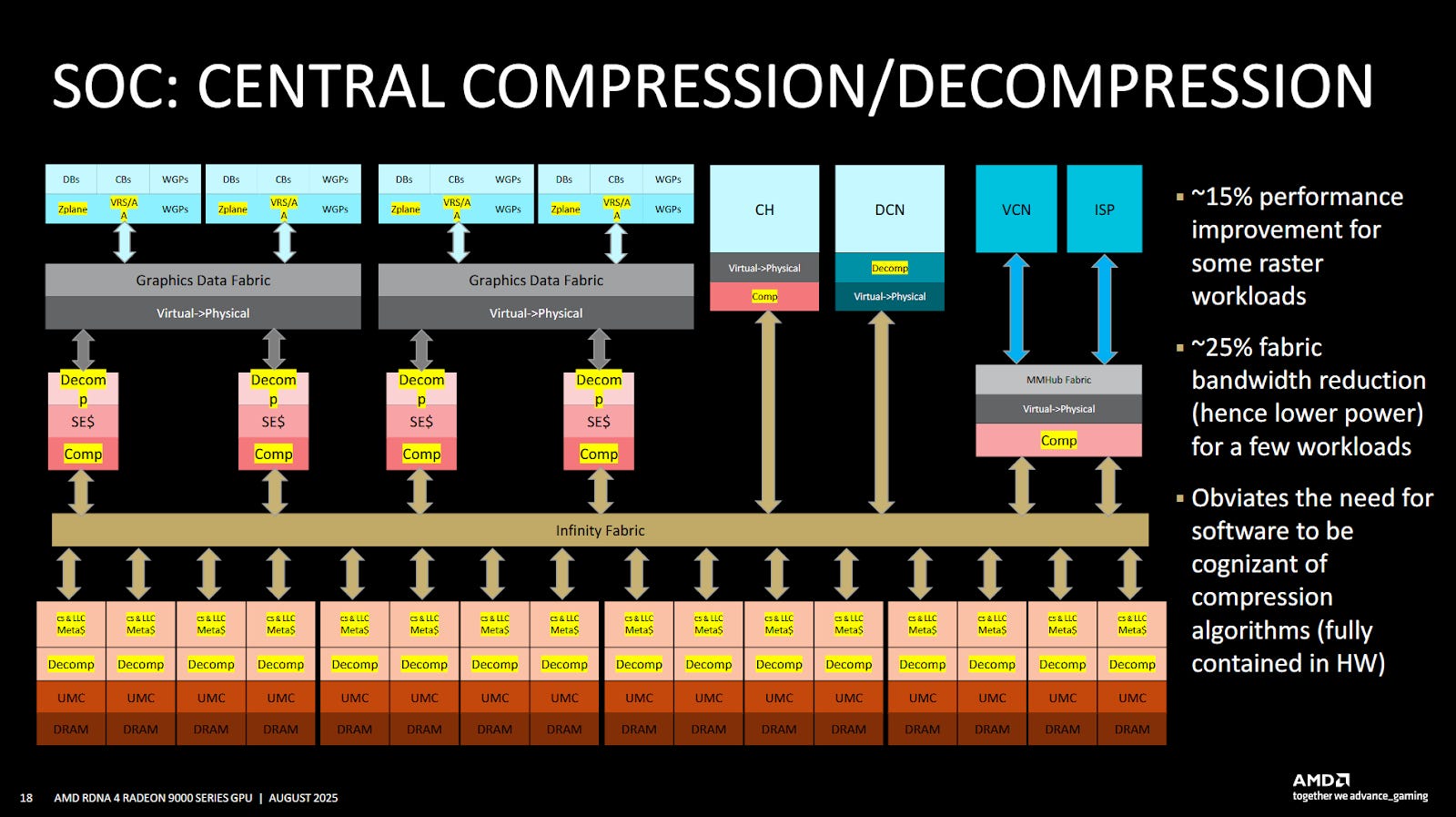
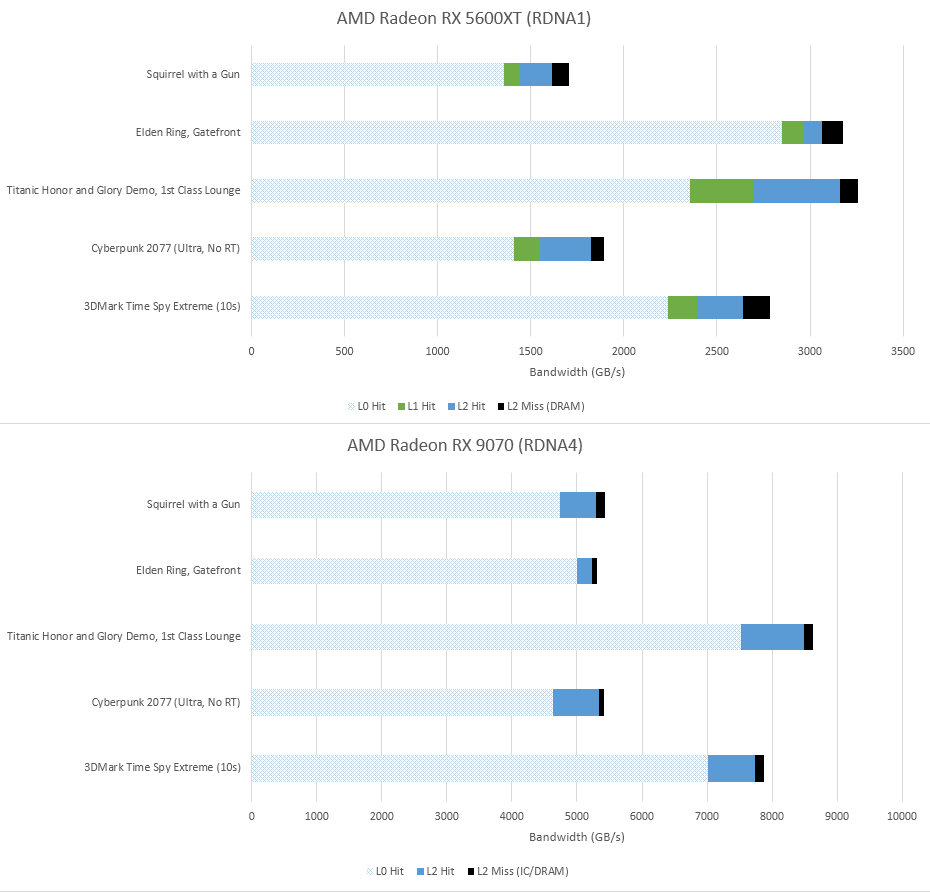
Transparent compression is not a new feature. It has a long history of being one tool in the GPU toolbox for reducing memory bandwidth usage, and it would be difficult to find any modern GPU without compression features of some sort. Even compression in other blocks like the display engine have precedent. Intel’s display engines for example use Framebuffer Compression (FBC), which can write a compressed copy of frame data and keep fetching the compressed copy to reduce data transfer power usage as long as the data doesn’t change. Prior RDNA generations had compression features too, and AMD’sdocumentation summarizes some compression targets. While AMD didn’t talk about compression efficiency, I tried to take similar frame captures using RGP on both RDNA1 and RDNA4 to see if there’s a large difference in memory access per frame. It didn’t quite work out the way I expected, but I’ll put them here anyway and discuss why evaluating compression efficacy is challenging.
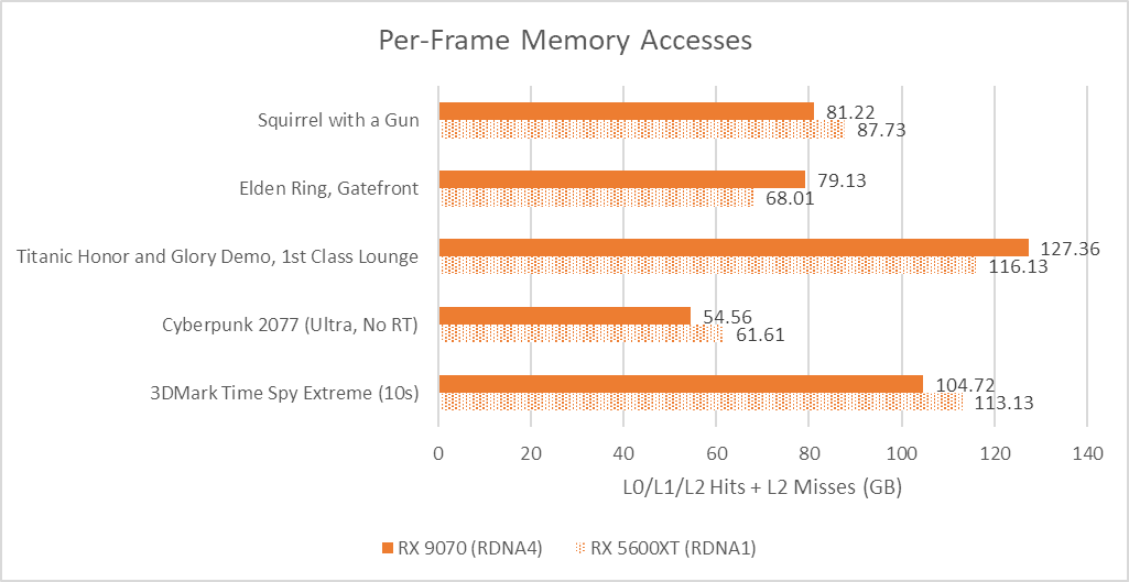
The first challenge is that both architectures satisfy most memory requests from L0 or L1. AMD slides on RDNA1 suggest the L0 and L1 only hold decompressed data, at least for delta color compression. Compression does apply to L2. For RDNA4, AMD’s slides indicate it applies to the Infinity Cache too. However, focusing on data transfer to and from the L2 wouldn’t work due the large cache hierarchy differences between those RDNA generations.
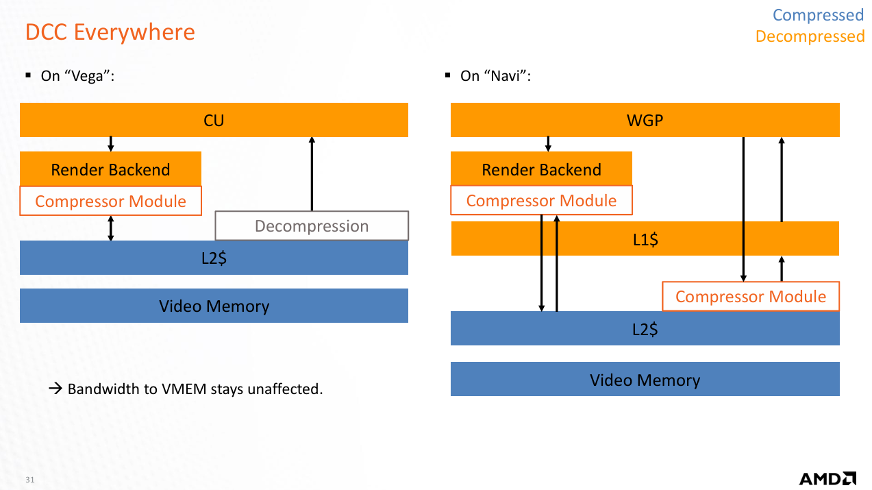
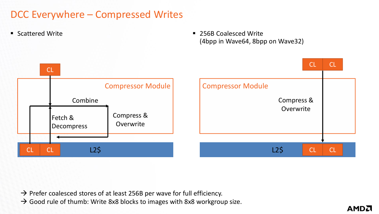
Another issue is, it’s easy to imagine a compression scheme that doesn’t change the number of cache requests involved. For example, data might be compressed to only take up part of a cacheline. A request only causes a subset of the cacheline to be read out, which a decompressor module expands to the full 128B. Older RDNA1 slides are ambiguous about this, indicating that DCC operates on 256B granularity (two cachelines) without providing further details.
In any case, compression may be a contributing factor in RDNA4 being able to achieve better performance while using a smaller Infinity Cache than prior generations, despite only having a 256-bit GDDR6 DRAM setup.
SoC Features
AMD went over RAS, or reliability, availability, and serviceability features in RDNA4. Modern chips use parity and ECC to detect errors and correct them, and evidently RDNA4 does the same. Unrecoverable errors are handled with driver intervention, by “re-initializing the relevant portion of the SoC, thus preventing the platform from shutting down”. There’s two ways to interpret that statement. One is that the GPU can be re-initialized to recover from hardware errors, obviously affecting any software relying on GPU acceleration. Another is that some parts of the GPU can be re-initialized while the GPU continues handling work. I think the former is more likely, though I can imagine the latter being possible in limited forms too. For example, an unrecoverable error reading from GDDR6 can hypothetically be fixed if that data is backed by a duplicate in system memory. The driver could transfer known-good data from the host to replace the corrupted copy. But errors with modified data would be difficult to recover from, because there might not be an up-to-date copy elsewhere in the system.
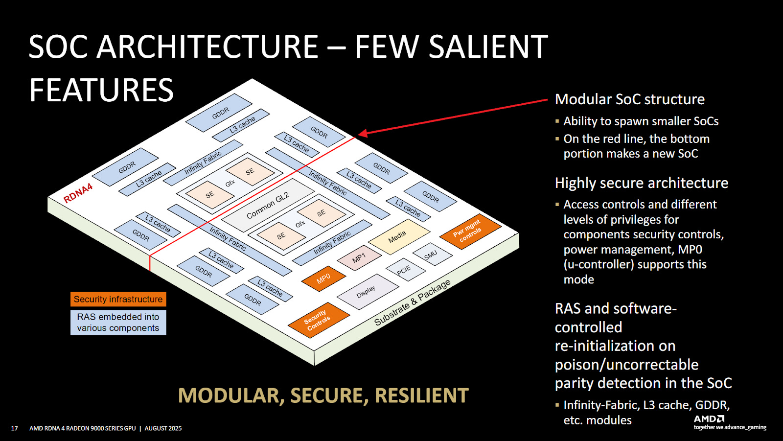
On the security front, microprocessors get private buses to “critical blocks” and protected register access mechanisms. Security here targets HDCP and other DRM features, which I don’t find particularly amusing. But terminology shown on the slide is interesting, because MP0 and MP1 are also covered in AMD’s CPU-side documentation. On the CPU side, MP0 (microprocessor 0) handles some Secure Encrypted Virtualization (SEV) features. It’s sometimes called the Platform Security Processor (PSP) too. MP1 on CPUs is called the System Management Unit (SMU), which covers power control functions. Curiously AMD’s slide labels MP1 and the SMU separately on RDNA4. MP0/MP1 could have completely different functions on GPUs of course. But the common terminology raises the possibility that there’s a lot of shared work between CPU and GPU SoC design. RAS is also a very traditional CPU feature, though GPUs have picked up RAS features over time as GPU compute picked up steam.
Infinity Fabric
One of the most obvious examples of shared effort between the CPU and GPU sides is Infinity Fabric making its way to graphics designs. This started years ago with Vega, though back then using Infinity Fabric was more of an implementation detail. But years later, Infinity Fabric components provided an elegant way to implement a large last level cache, or multi-socket coherent systems with gigantic iGPUs (like MI300A).
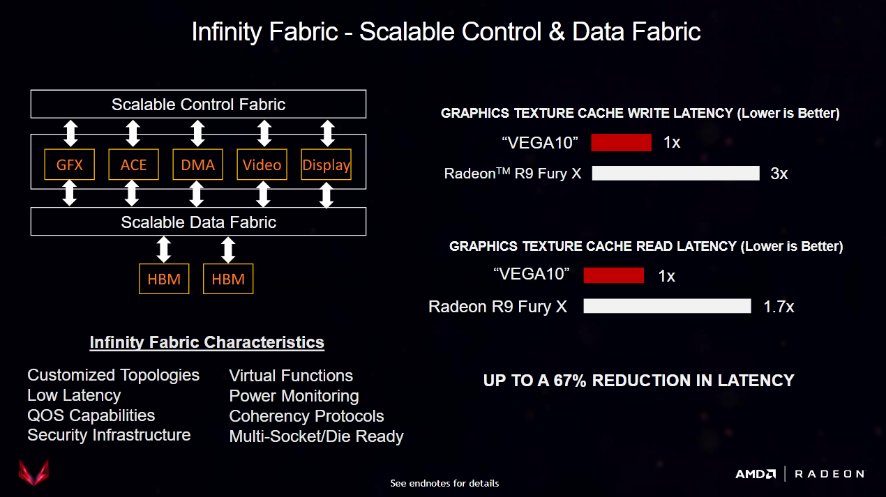
The Infinity Fabric memory-side subsystem on RDNA4 consists of 16 CS (Coherent Station) blocks, each paired with a Unified Memory Controller (UMC). Coherent Stations receive requests coming off the graphics L2 and other clients. They ensure coherent memory access by either getting data from a UMC, or by sending a probe if another block has a more up-to-date copy of the requested cacheline. The CS is a logical place to implement a memory side cache, and each CS instance has 4 MB of cache in RDNA4.
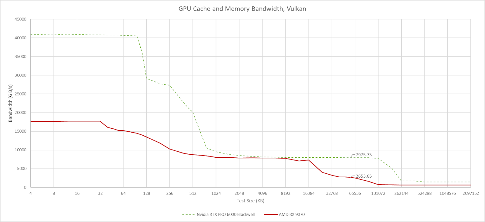
To save power, Infinity Fabric supports DVFS (dynamic voltage and frequency scaling) to save power, and clocks between 1.5 and 2.5 GHz. Infinity Fabric bandwidth is 1024 bytes per clock, which suggests the Infinity Cache can provide 2.5 TB/s of theoretical bandwidth. That roughly lines up with results from Nemes’s Vulkan-based GPU cache and memory bandwidth microbenchmark.
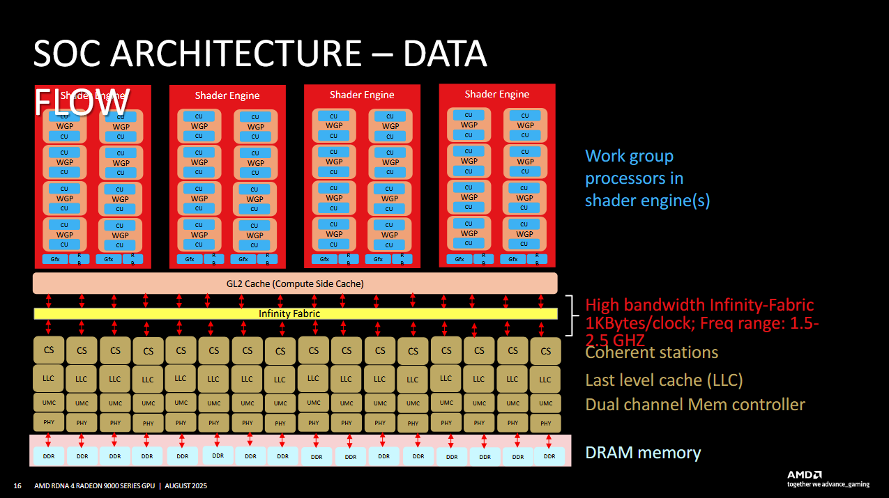
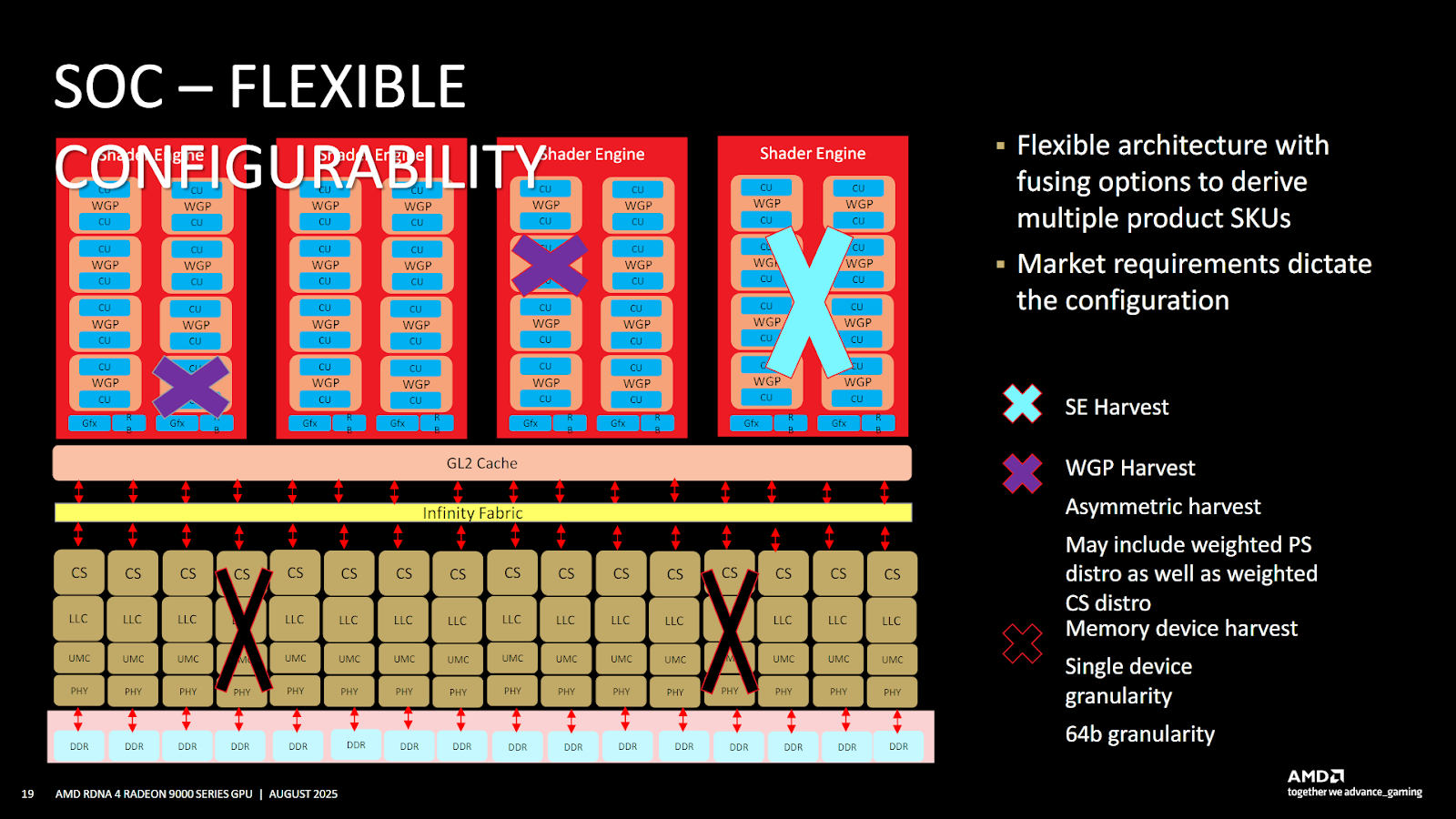
AMD also went over their ability to disable various SoC components to harvest dies and create different SKUs. Shader Engines, WGPs, and memory controller channels can be disabled. AMD and other manufacturers have used similar harvesting capabilities in the past. I’m not sure what’s new here. Likely, AMD wants to re-emphasize their harvesting options.
Finally, AMD mentioned that they chose a monolithic design for RDNA4 because it made sense for a graphics engine of its size. They looked at performance goals, package assembly and turnaround time, and cost. After evaluating those factors, they decided a monolithic design was the right option. It’s not a surprise. After all, AMD used monolithic designs for lower end RDNA3 products with smaller graphics engines, and only used chiplets for the largest SKUs. Rather, it’s a reminder that there’s no one size fits all solution. Whether a monolithic or chiplet-based design makes more sense depends heavily on design goals.
Final Words
RDNA4 brings a lot of exciting improvements to the table, while breaking away from any attempt to tackle the top end performance segment. Rather than going for maximum performance, RDNA4 looks optimized to improve efficiency over prior generations. The RX 9070 offers similar performance to the RX 7900XT in rasterization workloads despite having a lower power budget, less memory bandwidth, and a smaller last level cache. Techspot also shows the RX 9070 leading with raytracing workloads, which aligns with AMD's goal of enhancing raytracing performance.
AMD achieves this efficiency using compression, better raytracing structures, and a larger L2 cache. As a result, RDNA4 can pack its performance into a relatively small 356.5 mm² die and use a modest 256-bit GDDR6 memory setup. Display and media engine improvements are welcome too. Multi-monitor idle power feels like a neglected area for discrete GPUs, even though I know many people use multiple monitors for productivity. Lowering idle power in those setups is much appreciated. On the media engine side, AMD’s video encoding capabilities have often lagged behind the competition. RDNA4’s progress at least prevents AMD from falling as far behind as they have before.
If you like the content then consider heading over to the Patreon or PayPal if you want to toss a few bucks to Chips and Cheese. Also consider joining the Discord.
Thanks Chester!
The significant improvement in the efficiency of the display engine is (IMHO) also important in view of the rather limited capabilities of the iGPU of desktop Zen5 Ryzens (As opposed to the strong iGPUs in "Ryzen AI" APUs). I doubt that many people would use even an entry level Zen5 CPU without pairing it with a dGPU even if not primarily used for gaming. And having a display engine with good efficiency plus upgraded encode and decode ASICs for video makes the RDNA4 GPUs even more of a believable alternative to 5060s and 5070s Blackwell GPUs.
Thank you for this article!
I don't understand the advantage of split barriers. If I’m thinking correctly, the same performance can be achieved with normal barriers, just with a different instruction order.
Am I thinking about this correctly?