Correction on Qualcomm iGPUs
I wrote about Qualcomm iGPUs in three articles. All three were difficult because Qualcomm excels at publishing next to no information on their Adreno GPU architecture. Therefore, I went after Linux and Mesa source code for details. I also tried to infer what the architecture looked like via microbenchmarking. Both methods are time consuming and error prone. Code can be hard to read unless you’re intimately familiar with what it’s trying to do. Microbenchmarking is subject to stupid coding mistakes, and won’t tell you what Qualcomm calls hardware components under the hood.
A Mesa/Turnip developer kindly reached out and helped clear some of my confusion.
Command Processor
A GPU’s command processor takes commands from the CPU and sets up various GPU hardware blocks to get that work done. Adreno’s command processor actually consists of microcontroller(s) running a MIPS-inspired instruction set starting from the 5xx generation. Even though 5xx’s command processor moved away the instruction set used by AMD’s R600, it retained a similar ME+PFP arrangement.
Specifically, the command processor internally has two microcontrollers, A PreFetch Parser (PFP) takes host commands and can process simple commands on its own. Earlier, I thought the ME and PFP both directly read the command stream. Instead, only PFP reads the command stream, and passes commands to ME through a queue. Because PFP can run far ahead of ME, the two occasionally have to be brought back into sync by waiting for the queue between them to drain.
Adreno 6xx unifies the ME and PFP into a single “SQE” microcontroller, and adds a separate LPAC microcontroller to handle low priority compute. The previous diagram was accurate enough, as it’s a pretty simple change.
Optimizing Tiled Rendering
Tiled rendering tries to save memory bandwidth by splitting the screen into rectangular tiles and rendering them one at a time. Each tile is sized to fit within on-chip memory (GMEM), so intermediate writes don’t consume cache and DRAM bandwidth.
But tiled rendering requires more command processor effort. An immediate mode renderer can go over a list of draw calls once and draw everything as it goes. A tiled renderer with the screen hypothetically split into four tiles would repeat the process five times: once to figure out what’s visible in each tile and write that information to memory (binning), and once for each of the four tiles to render them.
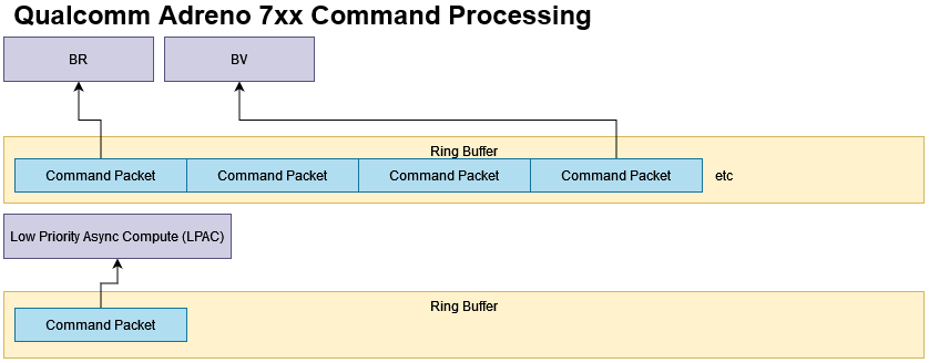
Adreno 7xx tries to speed up this work by introducing concurrency in the command processor. Adreno 6xx’s SQE gets split into two microcontrollers, called BV and BR. BV handles the binning pass, and BR renders the tiles. Obviously tile rendering has a dependency on binning, but the binning process for subsequent render passes can happen while BR is crunching through tiles. The driver emits thread control commands that tell BV and BR when they should start processing commands, and when they should skip them because the other microcontroller will handle them.
With BV and BR, Adreno 7xx gets a dual core command processor of sorts, but there are limitations. Concurrent binning requires driver support. BV can’t move too far ahead of BR, or visibility streams would start piling up and consume too much memory.
A better diagram for the Adreno 7xx’s command processor would have both BV and BR reading from the same command stream, with BV generally moving ahead of BR for concurrent binning.

What’s a Shader Processor?
The limited info Qualcomm published suggested Shader Processors (SPs) were the lowest level subdivision, and each had a texture processor with an associated L1 cache. I therefore went about finding how many SPs an Adreno GPU had by counting texture cache instances (by segmenting a pointer chasing array).
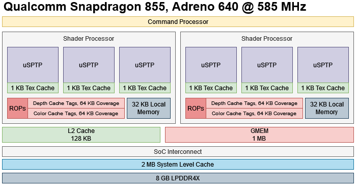
But what I thought was a SP is actually a uSPTP. uSPTP probably stands for Micro Shader Processor Texture Processor. A Shader Processor can have multiple uSPTPs, and all uSPTPs within a SP share a render backend (ROP). In that sense, a Shader Processor is a higher level subdivision akin to an Intel iGPU’s slice, or a Shader Array on AMD. The Shader Processor also supports its ROP with a Color Cache Unit (CCU), though confusingly the CCU only has tags for color and depth caches. The driver allocates color and depth caches per-CCU out of GMEM for immediate mode rendering.
That didn’t matter for Snapdragon 821’s Adreno 530, because each Shader Processor only had one uSPTP.
But later generations do have more than one uSPTP per Shader Processor. Therefore, the Snapdragon 8+ Gen 1’s Adreno 730 should look like this:
And the Snapdragon 855’s Adreno 640 should look like this:
Adreno 640 FP16 Throughput
When testing Adreno 640, I was surprised to not see double rate FP16 execution. After all, the two other Adreno GPUs I tested before did execute FP16 twice as fast as FP32. Connor told me I’m wrong, and Adreno 640 has a pair of 64-wide FP32 ALUs and a pair of 128-wide FP16 ALUs like other Adrenos. A FP32 wave128 instruction executes over two cycles, while a FP16 wave128 instruction would execute over a single cycle. Fully utilizing the FP16 ALU requires wave128, but wave128 might not be used if a kernel has too many live registers.
I used vectors in my GPU instruction rate testing to expose parallelism within each thread, because some GPUs (Terascale) benefit from it. However, that would increase register pressure. I redid the test with half scalar datatypes instead of half16, hoping to reduce register usage. I got slightly better results. Even though throughput is nowhere near double, it’s enough to convince me Adreno 640 indeed has wider FP16 units.
If I divide throughput by uSPTP clocks (585 MHz * 6x uSPTPs), then each uSPTP is able to execute roughly 128 FP32 operations per cycle. That aligns with it having two 64-wide FP32 ALUs. Doing the same with FP16 shows that each uSPTP is executing more than 2×64 FP16 ops per cycle, so the uSPTP does have wider FP16 units. I also tested inverse square roots, and those execute at double rate with FP16.
To correct the previous article, Adreno 640 does have double rate FP16 execution. I just had a hard time squeezing it out of the GPU.
Adreno 640 Scheduler Layout
I used Mesa’s fibers_per_sp to infer Adreno’s scheduler layout, and that was a confusing 128 * 4 * 16. That implies wave128, multiplied by 16 scheduler entries, multiplied by 4 uSPTPs. I was confused by that because there were three uSPTPs per SP, but Connor cleared it up. It’s simply rounded up to 4 because of how hardware calculates private memory offsets. Therefore, each uSPTP should be capable of tracking 16 wave128 threads, or 8 per ALU partition.
To summarize, Adreno’s uSPTPs should look like this:
Final Words
I originally started writing articles because I felt tech review sites weren’t digging deep enough into hardware details. Even when manufacturers publish very little info, they should try to dig into CPU and GPU architecture via other means like microbenchmarking or inferring details from source code. A secondary goal was to figure out how difficult that approach would be, and whether it would be feasible for other reviewers.
Adreno shows the limits of those approaches. GPUs are much harder to microbenchmark on a limited time budget because they’re not practical program using assembly code. Test code is thus subject to the whims of the driver and compiler. Furthermore, Qualcomm has documented just about nothing on their GPU architecture. Therefore, a lot of information has to be inferred by reading code and seeing how the hardware behaves with microbenchmarks. It’s very time consuming, and very error prone.
With that in mind I can’t fault more established tech sites for not digging into Adreno GPUs. They have to publish quickly and publish often. That leaves no room for the kind of time and effort needed to dig into an almost undocumented GPU architecture.
Finally, I’d like to thank Connor for clearing up the my confusion, especially with the tiled rendering process. I’ve learned a lot about how Adreno approaches it, along with the difficulties involved. I encourage anyone who wants a low level look at how tiled rendering works to look at the process at https://gitlab.freedesktop.org/mesa/mesa/-/blob/main/src/freedreno/vulkan/tu_cmd_buffer.cc.
If you like our articles and journalism, and you want to support us in our endeavors, then consider heading over to our Patreon or our PayPal if you want to toss a few bucks our way. If you would like to talk with the Chips and Cheese staff and the people behind the scenes, then consider joining our Discord.


