
Intel’s Dunnington: Core 2 Goes Dun Dun Dun

After Conroe’s launch in 2006, Intel had an excellent core architecture (Merom). They smacked AMD around in the client space where single threaded performance was king. But in the server market, multithreaded performance is extremely important. There, AMD still held the advantage because their HyperTransport point-to-point interconnect let them scale to large multi-socket configurations. Intel still primarily used a Front-Side Bus (FSB) architecture to connect CPUs to memory and each other, and a shared bus does not scale well to high core counts. On top of that, Merom was natively a dual core design. Penryn, the 45nm die shrink of Merom, offered increased L2 cache capacities and other tweaks, but did nothing to improve scaling to higher core counts.
Dunnington is Intel’s attempt to fight AMD in the server arena. They stuffed as many Penryn cores as they could onto a giant die. Then, they tried to work around FSB limitations with 16 MB of cache and an uncore architecture. This isn’t the first time Intel tried to scale up core counts by using a large L3. Tulsa uses a 16 MB L3 and a similar uncore architecture to shield two Netburst cores from FSB bottlenecks. But Dunnington is Intel’s first attempt at creating a very high core count die with an architecture that wasn’t plagued by a laundry list of terrible inefficiencies.
We’ll also use this article to cover the Merom/Penryn microarchitecture. Perom and Penryn are very scaled up P6 derivatives, making their architecture very different from that of their Netburst predecessors.
Dunnington Overview
Dunnington contains three dual core Penryn modules, each with 3 MB of L2 cache. In the center of the die, a Cache Bridge Controller (CBC) acts as the intra-die interconnect, and handles communications between the cores, L3 cache, and FSB. Unlike other CPUs, the FSB interface is located close to the center of the die to put it as close to the CBC as possible and thus allow high FSB speeds. But even a 1066 MT/s FSB will struggle to feed six Penryn cores, so Intel spends a significant amount of area implementing a 16 MB shared L3 cache.
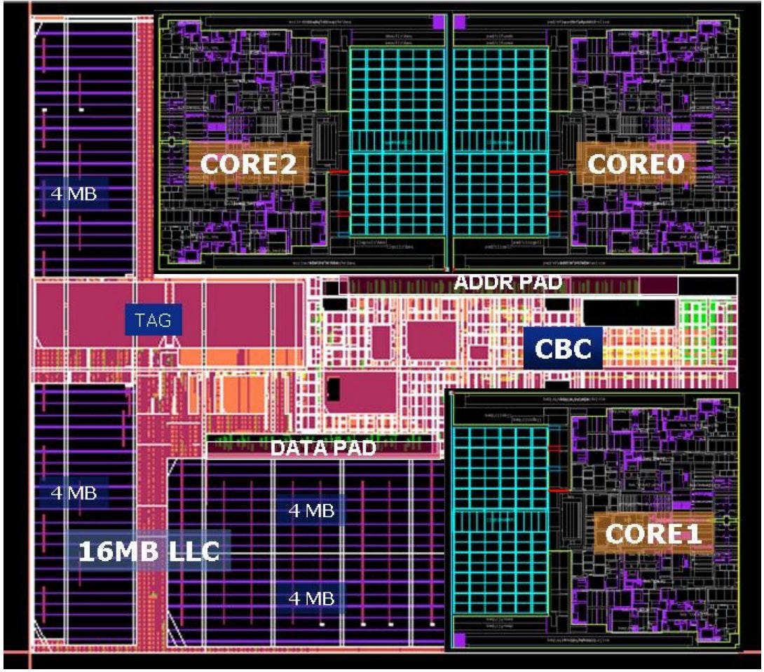
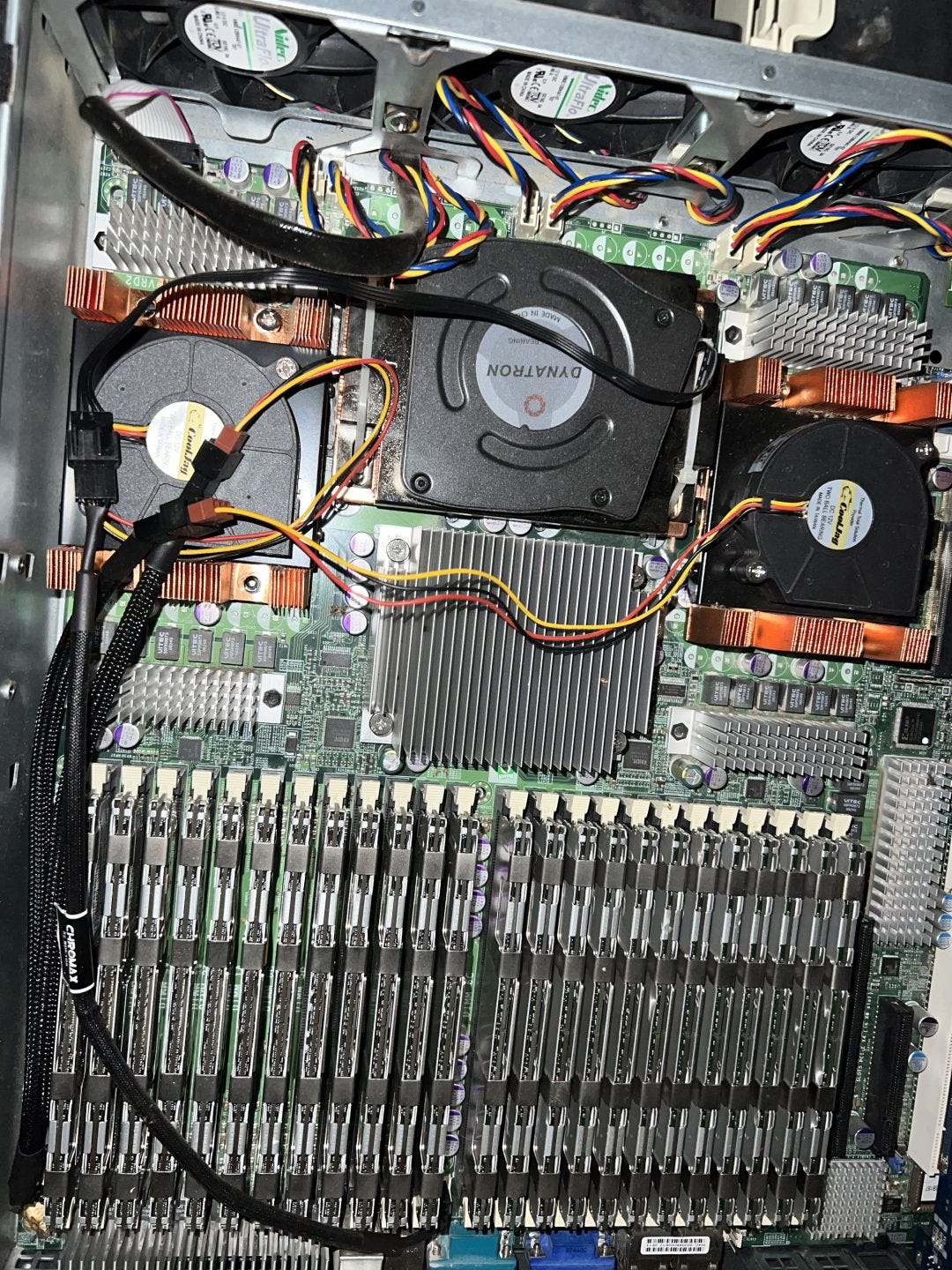
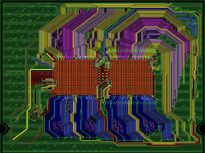
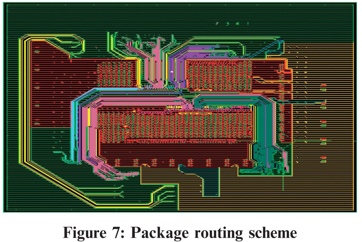
Dunnington is fabricated on Intel’s 45 nm process, and occupies an astounding 503 mm2 of area with 1.9 billion transistors. Tulsa was no joke either, with a 435 mm2 die and 1.328 billion transistors on Intel’s 65nm process. But Dunnington takes things a step further. For perspective, a Penryn die with 6 MB of L2 occupies only 107 mm2, and has 410 million transistors. Even with such a large die, Intel had to pull plenty of tricks to make everything fit. Vertical L3 blocks were implemented differently from the horizontal ones, creating an irregular L3 shape.
Core Block Diagram
Penryn is a 45nm die shrink of Merom, and represents a massive evolution of Intel’s P6 architecture. It’s wider, deeper, and more advanced than its Core Solo and Pentium M predecessors in the P6 line. Merom also adds 64-bit execution to P6, and Penryn carries that forward. Despite these huge advances, Penryn still retains some distinct P6 characteristics like a large, unified scheduler and ROB+RRF out-of-order execution scheme.

In a lot of areas, Penryn looks smaller and less sophisticated than Netburst. But unlike Netburst, Merom and Penryn execute very well on the fundamentals. They have large, low latency caches. Penalties for various difficult cases are mostly sane, unlike on Netburst.
Frontend: Branch Predictor
Compared to more modern CPUs, Penryn has a modest direction predictor. It looks a bit like the ones on low power CPUs from the mid 2010s. The direction predictor doesn’t seem quite as powerful as Netburst’s, but Penryn also has far lower mispredict penalties. Netburst’s mispredict penalty is even higher than what Intel’s published pipeline length suggests, because it’s unable to cancel erroneously fetched instructions after a mispredicted branch, and is forced to crunch through them.
Branch predictors have to be fast as well as accurate. To provide branch targets quickly, Penryn has a 2048 entry BTB. Penryn can also handle up to four taken branches with no pipeline bubbles. In one sense, that’s a regression compared to Netburst, because Netburst could handle over 1024 branches with 1 cycle latency. However, Penryn does far better after a first-level BTB miss. The 2048 entry BTB only suffers one penalty cycle. BTB miss penalties vary depending on branch distance, but are actually comparable to Netburst’s main BTB latencies.

Compared to AMD’s K10 and K8, Penryn has a notable advantage in being able to handle taken branches back to back. It can only handle four branches with that kind of speed, but that’s much better than nothing and means that loop unrolling isn’t quite as critical on Penryn.

Penryn therefore has a decent branch predictor for a high performance CPU in the late 2000s. Prediction accuracy is worse than that of modern desktop CPUs. But even a mediocre branch predictor can go a long way, and Penryn’s is still good enough to correctly predict the vast majority of branches. A mispredict also doesn’t hurt as much, because Penryn can’t have as much work in flight. K10 is in the same boat, but suffers in the speed department because it can’t do back to back taken branches.
Frontend: Instruction Fetch
Like prior P6 CPUs, Penryn uses a conventional 32 KB L1 instruction cache. Compared Pentium M, the decoders are now 4-wide instead of 3-wide. Funny enough, Intel originally wanted to make P6 4-wide, but realized they could get better overall performance with a higher clocked 3-wide core. Against Netburst’s trace cache, Penryn’s L1 instruction cache is more vulnerable to fetch bandwidth bottlenecks. But as long as instruction lengths remain relatively short, Penryn should see higher frontend bandwidth. The conventional instruction cache can also make much better use of x86’s instruction density, and efficiently make use of caching capacity.
Even though Penryn has a wide, conventional decoder, the core is still quite slow at running code out of L2. After a L1i miss, the core can’t exceed 1 IPC even with 4 byte instructions.
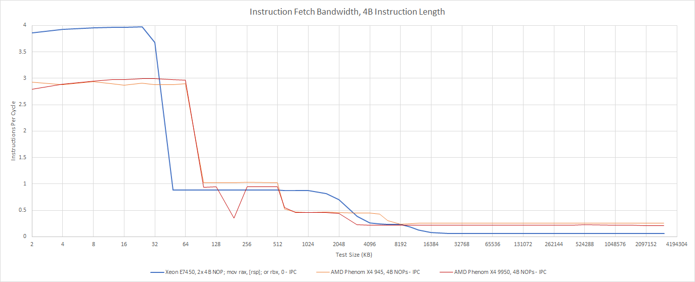
K10’s behavior is similar, though AMD benefits from having a larger instruction cache and is therefore less likely to suffer L2 code fetch penalties. As code footprints get even larger, the two architectures trade blows.
If code spills out of caches completely, Dunnington suffers compared to K10. Client Penryn isn’t nearly as bad and achieves rough parity with K10 when fetching instructions from DRAM.
Rename
Penryn’s renamer can break dependencies when it recognizes zeroing idioms, but can’t completely eliminate them. Even when an instruction is guaranteed to zero out a register, it still needs to go down an ALU pipe. K10’s renamer is similar, so Penryn really isn’t at a disadvantage unless we compare against much newer CPUs.
As we’d expect for CPUs of this era, Penryn and K10 both lack move elimination. The renamer on these old CPUs isn’t that exciting. Besides zeroing idiom recognition, it basically does register renaming the way you’re taught in computer science class.
Out of Order Execution
For its time, Penryn has a rather large out of order execution engine. Its headline 96 entry ROB capacity is already quite good. ROB capacity on these old CPUs also goes a bit farther than it does on modern CPUs, because the ROB+RRF setup means the ROB acts as a renamed register file. Because each instruction writes its result into its own ROB entry, there’s no way to run out of renamed register file capacity before running out of ROB entries.
On paper, Netburst has more reordering capacity, with a massive 126 entry ROB and large register files to back it up. But Netburst has to waste it tracking bogus instructions, and needs that reordering capacity to deal with some insanely high penalties. AMD’s K10 is a better comparison, because both architectures have reasonable penalties.

In most areas, Penryn has a substantial advantage in how many instructions it can keep in flight. The only exception is with 128-bit SSE operations, where AMD has an advantage because it doesn’t need to consume two registers to hold a 128-bit result. That could help K10 catch up in applications that heavily use 128-bit SSE vector operations.
Execution Units
Merom/Penryn get more execution resources to go with the core’s increased width. There’s an extra ALU pipe. Vector and FP units now natively handle 128-bit operations. For the most common operations, Penryn and K10 have very similar throughput. K10 still has an advantage in rarer integer operations like shifts, rotates, and LEAs.

Penryn also has very good floating point performance, as alluded to above. It’s a welcome improvement over Netburst and K8, which executed 128-bit floating point vector operations at half rate. Compared to K10, Penryn has matched FP throughput, but better FP addition latency. Integer vector addition is a bit different. There, Penryn has lower throughput than K10, but better latency. Intel can do a single 128-bit packed integer add per cycle, but with single cycle latency. AMD can do two per cycle at 2 cycle latency. The same applies to data movement between SSE registers. All three of K10’s FP pipes can handle 128-bit MOVs between registers, but again AMD suffers from 2 cycle latency for such a simple operation. Penryn can only do two per cycle, with 1 cycle latency.
Load/Store
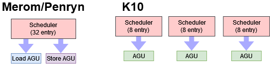
To execute memory operations, Penryn has two AGU pipes. Just like all CPUs in the P6 line, one AGU services loads, and the other services stores. This isn’t the best configuration, because loads typically outnumber stores by a large margin. The L1D can handle two accesses per cycle, but because of the AGU configuration, that can only happen when a load and store co-issue in the same cycle. In practice, the load pipe will probably see far higher utilization than the store pipe, and Penryn may find itself AGU limited. In contrast, AMD’s K8 and K10 have a hilariously overpowered AGU setup. There are three AGUs, all of which can handle load or store addresses. On AMD, the L1D is therefore more likely to be a bottleneck. It can handle two accesses per cycle. Both can be loads, and one can be a store.
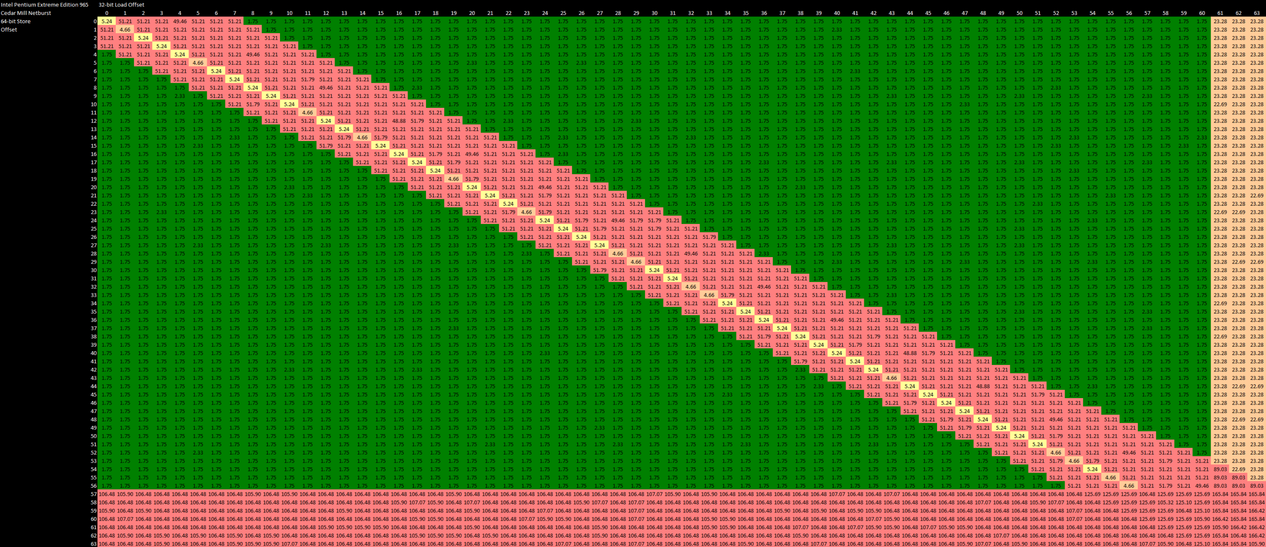
After generating addresses, the load/store unit has to make sure memory dependencies are satisfied. Loads might need to get their data from an prior in-flight store instead of the regular memory hierarchy, and the CPU has to check whether addresses overlap to determine that. Penryn generally does a good job in this area as long as addresses match exactly and the load doesn’t cross a 64B cacheline boundary. In those cases, store forwarding works with 5 cycle latency. Penryn can also forward the upper half of a store, as long as the store is 64-bit aligned.

If store forwarding fails, load latency increases to around 12 cycles. This failed store forwarding case can actually happen if the load and store don’t actually overlap, but access the same 64-bit aligned region. Strangely, Penryn can figure out that its initial dependency check screwed up, and back out early for a lower 2-3 cycle penalty if the load doesn’t cross a 64-bit boundary and the store address is greater than the load address. If the load address is greater, Penryn flips out and delays the load for 12 cycles even if there’s no true overlap. If the load and store overlap and cross a 64B cacheline boundary, the penalty increases to 22-23 cycles.
Netburst checks for memory dependencies on a finer granularity and doesn’t suffer from false dependency issues the way Penryn does. Forwarding only fails on Netburst if the store and load partially overlap, which means Intel’s older architecture has a rather robust memory dependency check mechanism. That’s great, except Netburst takes incredible 51 cycle penalties for failed store forwarding cases. And that penalty can increase to over 160 cycles if the load and store both cross a 64B cacheline.
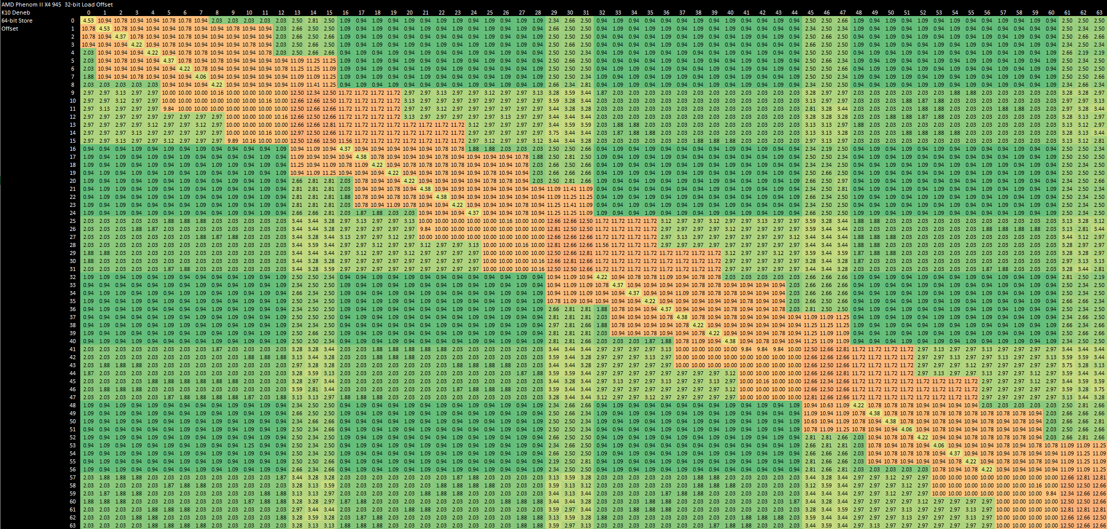
Like Penryn, AMD’s K10 uses pretty coarse checks for memory dependencies while suffering low penalties. Successfully forwarded stores have 4-5 cycle latency, and the failure case is generally 10-12 cycles. Forwarding works only for exact address matches, and doesn’t work if accesses are misaligned. Penryn can’t cope with misaligned accesses either, but it’s worse on K10 because AMD’s L1D is natively accessed in smaller blocks. Thankfully, K10’s penalty for misaligned, failed store forwarding attempts is lower at 12-13 cycles, or about half of Penryn’s.
Misaligned Access Penalties
CPU instruction sets give the illusion that you can directly address any byte of memory, but the L1D cache is typically addressed at a coarser granularity. When an instruction accesses a chunk of data that crosses a L1D alignment boundary, it typically takes at least two actual accesses to complete.
Penryn’s L1D is 64-byte aligned, and accesses that cross a 64 byte (512-bit) boundary suffer pretty harsh penalties. A misaligned store takes 10-11 cycles, and a misaligned load is even more expensive at 12-13 cycles. That’s better than Netburst, which suffers 22-23 cycle penalties for misaligned loads and 106 cycles for misaligned stores.
K10 accesses its L1D in 16 byte (128-bit) sectors, meaning that accesses are more likely to run into penalties. But K10 is quite good at handling misaligned accesses, taking just 2-3 cycles to deal with misaligned loads and stores.
4K Page Penalties
Penryn faces a very harsh 163 cycle penalty when a load crosses a 4K page boundary. Stores have it even worse, with a 218 cycle penalty. Meanwhile, K10 does not care if you cross a 4K page boundary. There’s no penalty beyond the misaligned access penalty mentioned above.
Some CPUs only check a subset of address bits when initially determining if memory accesses are independent. Specifically, they only check the offset into a 4K page. That makes sense, because the load/store unit gets virtual addresses from the AGUs. It won’t know the physical address until after a TLB lookup. And, checking higher virtual address bits doesn’t always tell you the entire story because two virtual pages could be aliased to the same physical one. This certainly applies to Penryn, which eats failed store forwarding penalties if accesses are 4096 bytes apart. Just like with store forwarding, this penalty also applies for accesses that touch the same 64-bit aligned block, spaced by a multiple of 4 KB. AMD’s K10 has similar issues with 4 KB aliasing, but the penalty is much lower at 3-4 cycles. It only goes up to 5-6 cycles for misaligned accesses, which is still much better than 12 cycles on Penryn.
I suspect Intel does a lot of checks at a very late pipeline stage. Page permissions certainly aren’t checked before reading data from cache, making the architecture vulnerable to Meltdown. Perhaps the full physical address is also not checked for memory dependencies until very late in the pipeline. If so, that would explain why Penryn suffers so hard from 4K aliasing. K10 in contrast recognizes the false dependence much earlier, resulting in a lower penalty.
Caching
On client systems, Penryn uses a two level caching system. The L1 cache is relatively small compared to the AMD competition, but similarly offers a pleasant 3 cycle load-to-use latency. Penryn’s L2 cache is both large and fast, and fills an important role in compensating for Intel’s then inferior DRAM performance.
But obviously, L2 miss traffic goes up when you have more cores, so Dunnington extends the cache hierarchy while still working within what Penryn was designed to do. Let’s start by looking at the caches present on all Penryn and Merom derivatives.
L1D Cache
Penryn and Merom have a 32 KB, 8-way L1D with 3 cycle latency. Like previous P6 CPUs, the L1D can service a load and a store per cycle, but Merom can handle 128-bit loads and stores with a single L1D access. The L1D is arranged into eight banks to allow servicing two accesses per cycle.

AMD’s K8 and K10 both have a larger 64 KB L1D with similar latency, but with only 2-way associativity. Compared to K8, Merom and Penryn have an advantage in vector code because K8 can only do one L1D access from the FPU per cycle, and further splits 128-bit accesses into two 64-bit ones. Penryn is at a L1D bandwidth disadvantage against K10, which can do two 128-bit loads per cycle, or one load and one store.
Penryn’s L1D therefore isn’t anything special. AMD’s L1D has similar latency but provides more bandwidth and twice as much capacity. But compared to Netburst’s 4 cycle, 16 KB write-through L1D, Penryn is a major step forward. Sometimes, not being a giant dumpster fire is exactly what you need to provide good, consistent performance.
L2 Cache
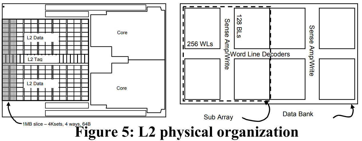
Penryn uses a 6 MB, 12-way L2 cache shared across two cores, which can be chopped to create a smaller 3 MB variant. The cache is physically implemented in 1 MB slices containing 4 ways, letting Intel flush and power down the cache in 1 MB chunks. Because the L1D cache will be handling the bulk of accesses, the L2 cache uses 0.38 um2 ULV cells to target high density and low power instead of high performance. That lets it operate at under 0.7V when active, and under 0.5V in standby.
On client systems, the L2 is the last level cache before hitting DRAM, and therefore has capacity comparable to the L3 caches in modern CPUs. For such a large cache, latency characteristics are excellent. Internally, the L2 has a 7 cycle pipeline starting from the L2 bus interface. Load-to-use latency appears to be about 15 cycles, putting it on par with K10’s smaller L2.

Compared to Merom, Penryn has 50% larger L2 size options, but seems to regress latency by one cycle. Both Core 2 generations therefore enjoy a very good combination of high L2 capacity with low latency. AMD’s 45nm K10 gives a single core similar total caching capacity, but uses a triple level cache setup to do so. Hitting the L3 cache on AMD gives much higher latency at almost 50 cycles. 65nm K10 is rather disappointing here, with only a 2 MB L3 that also takes around 50 cycles to access.
According to Intel, the L2 runs at core clock, and has a 256-bit bus that lets it handle a request every two clocks. We weren’t quite able to get 32 bytes per cycle even when loading both cores in a Penryn module.

One core seems to max out at 8 bytes per cycle, giving similar L2 bandwidth to AMD’s K10, though again with much better capacity. Loading both cores in a cluster pushes L2 bandwidth somewhat close to 16 bytes per cycle, but that’s still far off the 32 bytes per cycle that the L2 should be capable of. Still, Intel has a clear bandwidth advantage when servicing L1D misses, because AMD can pull less than four bytes per cycle from L3.
Overall, Penryn’s L2 cache provides an excellent combination of low latency and high capacity, even by today’s standards. L2 bandwidth is also plentiful considering Penryn’s modest vector throughput. On client and low core count server platforms, the L2 plays a large role in letting Intel beat out AMD.
Dunnington’s L3 Cache
Dunnington’s standout feature is a large, 16 MB L3 cache. On client and lower core count sever systems, Penryn dual core clusters directly connect to the chipset via a FSB interface. That works well enough with one or two clusters, but six cores are going to have a horrible time competitively sharing a FSB link. So, Dunnington adds a complex “uncore” subsystem that acts as a hub between the cores, L3 cache, and FSB interface. The uncore helps consolidate traffic from all three clusters onto one FSB link, and helps reduce off-die traffic by incorporating a 16 MB L3 cache.
To connect to the uncore, each Penryn cluster gets its FSB link replaced by what Intel calls the “Simple Direct Interface (SDI)”.

SDI first made its debut on Tulsa, where it linked Netburst cores to an on-die Cache Bridge Controller (CBC). The CBC acted as a central on-die hub connecting the cores to a 16 MB L3 cache, the FSB, and each other. Dunnington’s configuration is clearly derived from Tulsa, though there are now three SDI links, which connect to Penryn clusters instead of Netburst cores. Like Tulsa, Dunnington runs the L3 cache and other uncore components at half of the core clock.
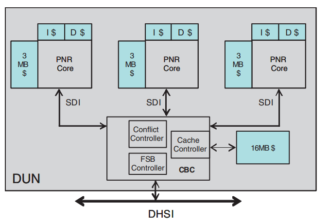
Physically, Dunnington’s 16 MB L3 is organized into 4 MB blocks, but the L3 is synchronous and all L3 accesses have the same latency regardless of which block they’re served from. The full 16 MB L3 is 16-way set associative, and capacity can be cut down by reducing the number of ways to 12 or 8. The Xeon E7450 we have access to implements 12 MB of L3 capacity with 12 ways. Intel uses 0.3816 µm2 bitcells to implement the L3 data array, while the tag array uses 0.54 µm2 bitcells. The L3 bitcells therefore aren’t denser than the L2 ones.

L3 latency is mediocre at around 37 ns, which is much higher than AMD’s L3 latency. Intel’s Hot Chips 18 presentation states that Tulsa has about 35 ns of L3 load to use latency. Dunnington’s uncore architecture is clearly derived from Tulsa’s, so the similarity is not surprising. Intel’s latency deficit is somewhat excusable considering the L3’s high capacity compared to AMD’s. Also, some modern server chips like Ampere Altra suffer about 35 ns of L3 latency, though that’s more the exception than the rule.

Bandwidth is lacking as well. With a 8 MB test size, a single core can only pull 8.2 GB/s from L3. Using both cores in the cluster gives us 9.49 GB/s. If we start loading all of the cores in a socket, the L3 basically disappears. That’s because the L3 is inclusive of upper level cache contents. If all three Penryn clusters are caching different data in their private 3 MB caches, only 3 MB of L3 capacity is useful.
Normally, we test with each thread reading from its own array. Testing with all threads reading from a shared array is problematic, because the memory subsystem can combine requests if multiple cores happen to request the same data. But testing with separate arrays for each thread is problematic for Dunnington, because we’ll see the sum of private cache capacities. Thankfully, numbers don’t seem to be too far off when using a shared array to test cache bandwidth. In this shared mode, Dunnington gets 38.35 GB/s of L3 bandwidth. For comparison, AMD’s Phenom X4 9950 gets 35.86 GB/s with the same methodology, and the Phenom II X4 945 gets 41.42 GB/s. On the X4 945, performance counters generally back up the bandwidth measurements in shared mode.
Tulsa’s L3 was even worse with 18.1 GB/s of read bandwidth, according to Intel’s slides. Dunnington’s L3 therefore has reasonable bandwidth, assuming there’s not a lot of request combining going on. It’s a dramatic improvement over Tulsa and isn’t too far off AMD. Still, that 38.35 GB/s is feeding six cores, and Dunnington’s cores will have to lean on the larger L2 to prevent bandwidth bottlenecks.
Intel made the L3 inclusive in order to have it serve double duty as a snoop filter for data cached on-die. In addition to storing data, the L3 keeps core-valid bits to track which module has a line cached. A L3 miss therefore implies that the data is not cached anywhere on the die, and the uncore should send a request to the chipset over the FSB.
Chipset
Dunnington’s 7300 chipset is built with scalability in mind, or at least tries very hard to cope with the demands of 24 Penryn cores. The memory controller hub (MCH) features four FSB links, giving each socket an independent link. To feed such a large CPU setup, Intel equipped the chipset with a quad channel DDR2 memory controller. In addition to memory access, the chipset is responsible for minimizing cross-socket snoops.

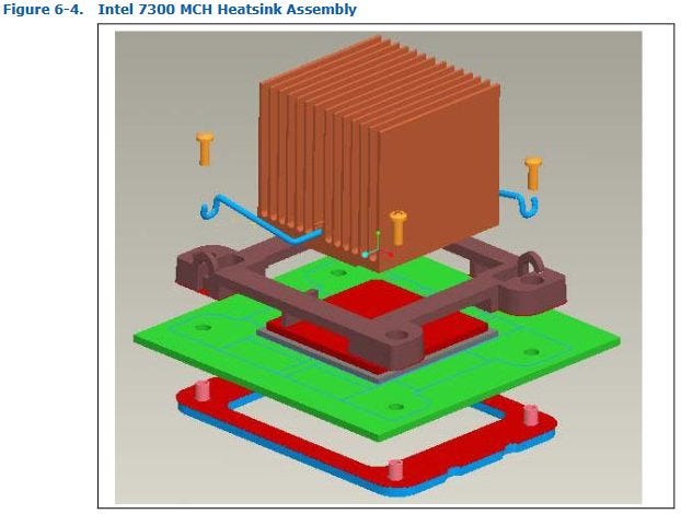
Physically, the chipset’s MCH is a monster. It’s implemented on a 12-layer, 2013 pin (ball) package that measures 49.5 mm on each side. Even though the MCH’s core clock is relatively low at 266 MHz, it consumes enough power to require a substantial heatsink.

In some ways, the MCH’s role is similar to that of AMD’s modern IO dies. From that perspective, the power consumption under load isn’t too extreme, especially considering the older process node.
For IO connectivity, the MCH has 28 PCIe 1.0 lanes, with four more dedicated lanes to connect to the southbridge.
Coherency Latency
On a small client or server system with a couple of Penryn core clusters, coherency traffic wouldn’t be a big deal and could be handled just fine over a shared FSB. But Dunnington is another monster. With three clusters per socket and four sockets in a system, you really want to avoid asking everyone if they have something cached.
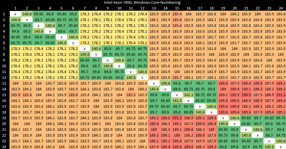
Dunnington therefore has two levels of snoop filters. The first is the L3 cache, as discussed earlier. Atomic operations generally have a latency of just under 70 ns when bouncing cachelines between modules within a die. Strangely, latency is higher when bouncing cachelines between two cores within the same Penryn module.
If a request misses L3, it goes over the FSB link to the 7300 chipset’s Memory Controller Hub (MCH), or northbridge. To support quad socket configurations without requiring sockets to share a FSB, the chipset has four independent FSB links. Obviously, Intel doesn’t want to defeat this optimization by having to broadcast snoops across those FSBs, so the MCH gets a substantial 1M entry, 128-way snoop filter to track data cached across all four sockets. The snoop filter is implemented as two interleaves, each with eight affinities.
The snoop filter tags alone take up 4.5 MB of storage on the MCH die, and are large enough to deal with Dunnington’s 40-bit physical address space. Modern CPUs have more physical address bits, but 40 bits are enough to address 1 TB of memory and installing anywhere near that much DRAM would be impossible in a Dunnington system.

Since each snoop filter entry tracks a 64 byte cache line, the MCH can track 64 MB of cached data. That’s enough to cover L3 contents on four fully enabled Dunnington CPUs. Snoop filter data consists of 5 bits per entry, which tell the MCH exactly which sockets to snoop.
The snoop filter is further organized into two interleaves, each of which are split into four affinity sets. Read-modify-write transactions are quite common on the snoop filter, because a socket might want to figure out the state of a cacheline and bring it into its caches. To efficiently handle such accesses, the snoop filter is hot-clocked at 533 MHz, or twice the MCH clock. Lookup latency for the snoop filter is 4 cycles, or 2.1 ns. Our core to core bounce test measures about 178 to 190 ns when data has to go across sockets.
AMD’s chipset northbridge (not to be confused with the on-die northbridge) in contrast is only responsible for handling IO connectivity. The on-die northbridge takes over most of the high bandwidth functions handled by Intel’s MCH. AMD takes a different approach to maintaining cache coherency. Space on the CPU die is quite valuable, so AMD can carve out part of the CPU’s L3 and use that as snoop filter. Because AMD has memory controllers and their associated on-die northbridges distributed across all sockets, each socket only reserves 1 MB of L3 capacity to implement snoop filter functionality. That 1 MB L3 partition then acts as a 256k entry, 4-way snoop filter capable of covering 16 MB of cached data. AMD’s snoop filter is addressed only by the offset into the socket’s DRAM base address, instead of the full physical address like on Intel.
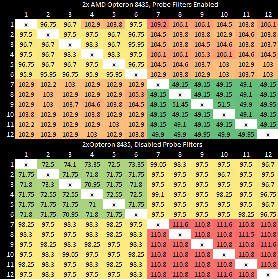
AMD generally achieves better latency when atomics have to bounce cachelines between cores. Within a socket, latencies are about 20 ns lower than Intel’s. Cross socket latences are around 100 ns, which is much better than the 170-190 ns we see on Dunnington. Even when Opteron CPUs aren’t set up to use part of their L3 as a snoop filter, performance is still quite reasonable with a worst case.
DRAM Performance
To feed 24 cores across four sockets, the chipset has a quad channel DDR2 controller. It supports fully buffered DIMMs to support up to 512 GB of memory capacity, with up to 8 DIMMs per channel. Maximum DDR2 speed is rather low at 667 MT/s, but in theory four channels should give the chipset plenty of memory bandwidth. In theory. In practice, bandwidth is absolutely terrible. A single socket can pull 2.3 GB/s from DRAM. Across all sockets, bandwidth maxes out at 8.64 GB/s. That’s a terrible result, considering a single socket K10 chip has more DRAM bandwidth.

Dunnington does achieve better bandwidth when all threads read from a shared array, while K10 gets about the same bandwidth. However, Dunnington’s memory controller could be combining accesses when multiple sockets happen to request the same data.
Unfortunately, three of the FBDIMMs in the system we had access to were broken. That would negatively affect memory bandwidth, especially if all of them were on one channel. Uneven capacities across channels would prevent accesses from being evenly striped across them. So we’re not going to put too much weight into this poor memory bandwidth result.
Final Words (Merom/Penryn)
Merom’s 2006 release represents an impressive comeback for Intel’s P6 architecture. Compared to Netburst, Merom has fewer flashy architectural features, but executes very well on the fundamentals. Penalties are generally low. Netburst might have a more advanced branch predictor, but Merom’s can provide more consistent speed. Furthermore, Merom doesn’t carry forward Netburst’s idiotic inability to cancel bogus instructions fetched after a mispredicted branch. That could inflate Netburst’s branch mispredict penalty to over 100 clock cycles, if a long dependency chain was erroneously fetched before a mispredict was discovered.
At the same time, the core is scaled up enough to beat AMD’s K8 and K10 on most key points. Advanced features like memory dependence prediction give it an advantage too. Intel doesn’t win in every last area, but many of K10’s advantages are found with rarer operations. Penryn’s cache setup deserves special praise. Intel achieves similar caching capacity to K10 with just two cache levels, meaning the core has less cache latency to deal with. Combine that with larger out-of-order execution buffers, and Penryn is a force to be reckoned with.
Zooming out, Merom and Penryn demonstrate that having low penalties and a low latency cache heirarchy are much more important than flashy architectural features. Of course, advanced branch predictors and dependency predictors help. Large OoO execution buffers help. But they aren’t good coping mechanisms for serious architectural flaws, as we saw with Netburst. Merom therefore served as a reset of sorts for Intel’s high end offerings. With Nehalem and Sandy Bridge, Intel slowly combined Netburst’s advanced features with the P6 line, creating products that AMD wouldn’t be able to match for years.
Final Words (Dunnington)
After Nehalem and Sandy Bridge, Intel held a commanding lead over AMD in both the client and server markets. Intel’s core microarchitecture was superior, of course, but Intel also owed their success at that time to a superior on-die interconnect. Nehalem’s uncore did quite well, providing better L3 performance than AMD until Zen’s launch. But Intel’s modern uncore architecture didn’t come out of nowhere, and Intel definitely struggled with uncore design in the early days. Dunnington is an example of this. Its uncore setup represents a transition point between older, purely FSB based designs, and modern Intel uncores designed with high core count performance scaling in mind.
Merom and Penryn were designed to excel in a consumer market where dual core setups represented a sweet spot between cost and performance. Like prior Intel architectures, higher core counts were handled by sharing the FSB interface. All CPU agents would have their FSB interfaces connected to the same set of physical wires, and the CPUs would arbitrate for FSB access to ensure fairness. Coherency was quite simple, because everyone could track every transaction being made on the FSB. For example, let’s say a CPU wanted to read from memory. The process would proceed something like this:
The CPU would wait for its turn to make a request on the FSB
Other CPUs would see the address on the FSB, and check their internal caches to see if they have the requested address cached
If another CPU had modified data at the requested address, that CPU writes the requested data back over the FSB
Otherwise, the memory controller puts the requested data on the FSB
This worked well enough as long as you didn’t have too many FSB agents. Merom and Penryn’s quad core configurations used two clusters on a shared FSB. Before that, Intel made dual core Netburst chips in a similar fashion.
But a shared FSB didn’t scale much farther. Paxville already suffered from high FSB utilization in certain applications, and Tulsa mitigated this by implementing a new uncore architecture. Dunnington extends what Tulsa started, replacing the Netburst cores with Penryn core clusters.
Unfortunately, none of this performed well. L3 latency is quite high by modern standards, and worse than L3 latency on competing AMD chips. Multithreaded performance scaling is distinctly non-ideal. We never expect perfect scaling for sure, because shared cache and memory bandwidth become increasingly serious bottlenecks as more cores get loaded. But for Dunnington, it’s quite poor.

Loading up two clusters within a Dunnington socket provides a 53% performance increase for a libx264 video encoding workload. That’s well short of the idea 100% speedup we’d expect from doubling core count. Loading up all six cores in the socket barely increases performance further, pointing to either a L3 or FSB bandwidth bottleneck. Hitting two sockets does almost double performance. But loading up more sockets appears to push us into a memory bandwidth bottleneck, because we start seeing diminishing gains again.

Despite all the efforts put into Dunnington, Intel still failed to beat AMD in multithreaded performance scaling. We needed two sockets and 12 cores to beat a quad core AMD chip.

But Intel had to start somewhere. In that sense, Dunnington represents a stepping stone towards Intel’s more competent uncore designs. Concepts pioneered in Dunnington and Tulsa, like the inclusive L3 with core/module valid bits, repeatedly showed up in Intel architectures through 2020. For sure, Intel swapped out a lot of things as they made improvements. SDI was replaced by IDI, and the CBC interconnect was replaced by first by a global queue in Nehalem, then by a ring bus in Sandy Bridge. Intel made a lot of progress.
The take away is that multithreaded performance is hard. It’s not as simple as copy-pasting cores around, because you need to design a good shared caches and a good interconnect to feed the cores. Memory bandwidth also needs to scale. Intel learned some hard lessons with Tulsa and Dunnington. They saw where their CPUs struggled, and relentlessly beat down those shortcomings to create Nehalem and Sandy Bridge.
If you like our articles and journalism and you want to support us in our endeavors then consider heading over to our Patreon or our PayPal if you want to toss a few bucks our way or if you would like to talk with the Chips and Cheese staff and the people behind the scenes then consider joining our Discord.