


AMD’s Zen 4, Part 2: Memory Subsystem and Conclusion

Please go through part 1 of our Zen 4 coverage, if you haven’t done so already. This article picks up where the previous one left off. To summarize, Zen 4 has made several moves in the frontend and execution engine meant to increase utilization of existing execution resources, which remain largely unchanged since Zen 3 and even Zen 2. Now, we’re going to look at the memory subsystem, from the data side’s perspective.
Memory Execution
Like Zen 3, Zen 4 uses three AGUs to calculate addresses for load and store instructions. These addresses, along with store data if applicable, are passed to the load/store unit. The load/store unit then has to face the complicated job of making sure memory accesses appear to execute in program order, while extracting as much performance as possible.
High performance means keeping a lot of operations in flight to hide memory access latency, and the load/store unit has to do its role by tracking pending memory operations. To do this, Zen 4 implements a large load queue. Since Zen 1, AMD’s load queue works differently than Intel’s. After a load operation receives data, the load queue is free to de-allocate it. A separate, larger structure is used to track load operations through to retirement. To differentiate these structures, we’ll call the larger structure a “load validation queue”, and the published load queue the “load execution queue”. Separating out these structures lets AMD keep 136 load operations in flight, way more than their published load queue size would suggest
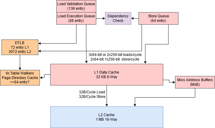
Stores on Zen 4 have to be buffered in a relatively small 64 entry store queue. This store queue sees even more pressure with AVX-512 code, since a 512-bit store will consume two store queue entries.
Once memory operations are in their respective queues, the load/store unit has to make sure memory ordering is preserved. If an in-flight store has an address that overlaps with a newer load’s, the store’s data can be forwarded to the load. Like Zen 3, Zen 4 can do store forwarding with no latency. That is, a chain of dependent loads and stores will execute at 2 IPC.
However, terms and conditions may apply. The load and store addresses must match exactly. An extra 1 cycle latency penalty is assessed if the store crosses a 32 byte aligned boundary. The mechanism fails completely if the store crosses a 4 KB aligned page boundary.
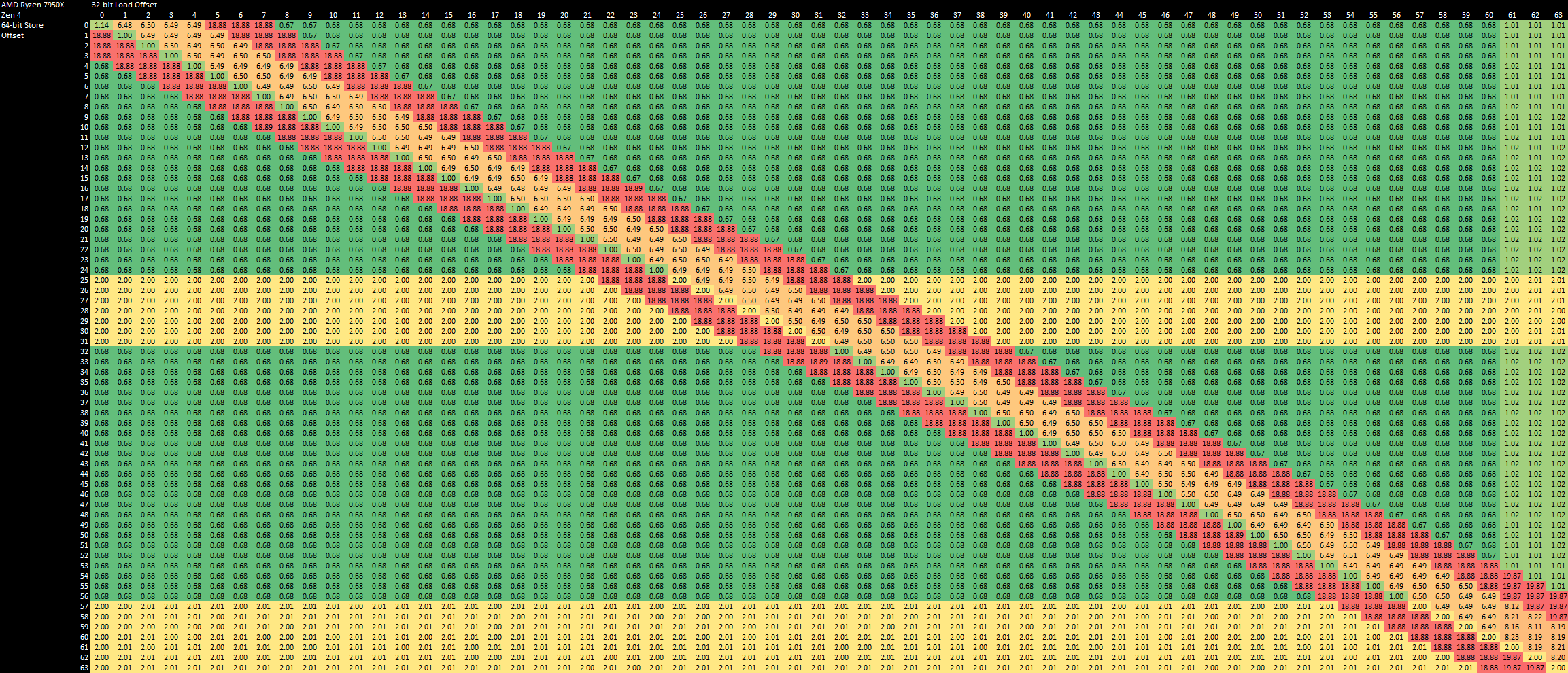
Partial overlap cases where the load is completely contained within the store are handled with a latency of 6-7 cycles, which is a slight improvement over Zen 3’s 7-8 cycles. Store forwarding fails on both Zen generations if the load and store overlap, but the load can’t be completed with just data from the store. Zen 4 takes a 19 cycle penalty in this case, which probably corresponds with waiting for the store to retire and reading the data from L1D. In contrast, Zen 3 could handle the failure case in 18 cycles, but only if the store address is aligned to a 4 byte boundary. Otherwise, Zen 3 suffers a 25 cycle penalty, which Zen 4 avoids. To summarize reciprocal throughput for loads dependent on a store, for all the tested store forwarding cases:

Zen 4 retains most of Zen 3’s store forwarding characteristics, and improves slightly on the most common cases. There’s a slight regression on the less common page boundary crossing cases. Crossing a page boundary while handling a store forwarding case is extremely expensive on both architectures. It’s even more expensive than on Zen 1 and Zen 2, and is best avoided.
Golden Cove’s store forwarding enjoys slightly lower latency than Zen 4 for most cases, except when the load and store both cross a 64B cacheline boundary. For exact address match cases, Golden Cove enjoys a throughput advantage rather than a latency one. With four AGUs, Golden Cove can generate addresses for two loads and two stores per cycle.
For more common, non-overlapping loads, Golden Cove continues to have an advantage because the L1D is accessed in larger chunks, and will suffer from fewer misaligned accesses. We like to think of memory accesses as being byte addressable and totally random. But in practice, caches are addressed in larger, aligned chunks. “Aligned” here means the memory address is a multiple of a specific size. For example, the low 5 bits of a 32 byte aligned memory address will be zero. A “misaligned” access crosses an alignment boundary, forcing the load/store unit to make two L1D lookups to satisfy the request.
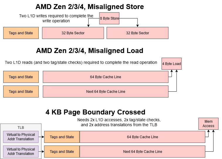
Golden Cove’s L1D handles loads and stores in 64 byte, cacheline sized blocks. AMD’s L1D in contrast handles writes in 32 byte blocks, starting with Zen 2. A write that crosses the boundary between two 32B blocks on Zen 4, or 64B blocks on Golden Cove, takes two cycles to complete. Zen 4 improves over Zen 3, which could take 5 cycles to handle such a misaligned load, and could only get the 2 cycle case if the store was also 4B aligned. Golden Cove, Zen 3, and Zen 4 also see reduced throughput for loads crossing a 64B boundary, though that case is handled better because load throughput is higher in the first place.
Accesses that cross a 4 KB boundary introduce more complications, because virtual to physical address translations are usually handled in 4 KB pages. Handling such an access would require accessing two TLB entries as well. All Zen generations handle this case without any more difficulty than the regular misaligned load case, indicating that their TLBs can service multiple lookups per cycle. Intel’s Golden Cove and Ice Lake architectures do incur a minor penalty when handling loads that cross a 4K boundary.

Writes carry massive penalties in all tested architectures. They’re especially heavy on Zen 4, even compared to prior Zen generations. I wonder if AMD found that split-page accesses were rare enough that a higher penalty was acceptable in exchange for higher clock speeds.
Cache and Memory Performance
Computing power has been steadily outpacing memory performance for the past three decades. CPUs in response have used increasingly complex cache setups to keep delivering performance increases. Intel and AMD’s high performance cores have settled on a triple level caching scheme. Each core gets a small L1 cache, and a modestly sized L2 cache to insulate it from L3 latency. The L3 cache is many megabytes in size, and shared across a set of cores.
Latency with 2 MB Pages
Let’s start by testing memory latency with 2 MB pages, to get an idea of the cache hierarchy from a single core’s point of view. Using 2 MB pages isn’t representative of how most applications will access memory, but it does make more efficient use of TLB capacity, and lets us look at cache latency and TLB penalty separately.
Zen 4’s caches closely resemble Zen 3’s. The biggest change is doubling L2 size to 1 MB, at the cost of 2 cycles of latency. That in turn also pushes L3 latency up two cycles.
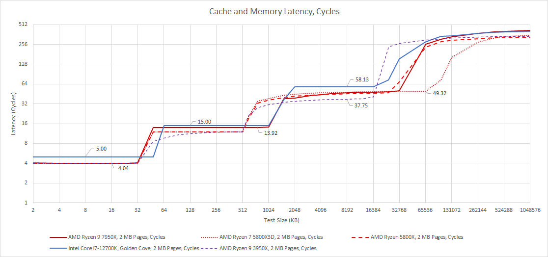
Intel’s Golden Cove has higher latency at all cache levels, though Intel’s core-private caches are slightly larger. Golden Cove’s L1D has 5 cycles of latency, or just one more cycle than Zen 4’s 4 cycles. One cycle might not seem like much, but that represents a 25% latency increase over AMD, and the L1D cache will be in the path of all memory accesses. The latency difference is smaller at L2, where Intel’s 1280 KB cache has 15 cycle latency against AMD’s 1024 KB, at 14 cycles. L2 will see far fewer accesses than L1, and a 1 cycle difference here is a much smaller difference percentage wise.
At L3, there’s a massive difference in latency. Intel does not run the ring at core clock, and has a longer ring that services two E-Core clusters as well as an iGPU. Golden Cove takes almost 20 more cycles to get data from its L3 than Zen 3 and Zen 4. So, Intel uses a larger L2 to shield the core from L3 latency, and gives Golden Cove massive reordering capacity to hide L3 latency.

If we look at true latency, Zen 4’s very high 5.7 GHz clock speed comes into play. We see incredibly low L1D latency at just 0.7 ns. L1D hitrate is typically over 80-90%, so most memory accesses will enjoy this very low latency. AMD’s new L2 is similarly impressive. Zen 4’s clock speed increase means that its L2 has slightly lower latency than the L2 in prior Zen generations.
Finally, AMD gets Zen 4’s L3 latency back down to the 8-9 ns range. Zen 3 had increased the amount of L3 accessible to a single core by unifying a L3 cache across eight cores and eight L3 slices, but incurred a latency penalty to do so. With Zen 4’s clock speed, L3 latency comes back down to Zen 2 levels, but with twice as much capacity. Zen 4’s L3 latency also pulls ahead of Zen 3’s V-Cache latency. However, Zen 3’s V-Cache variant holds a 3x advantage in cache capacity.
In memory, we see a reasonable latency of 73.35 ns with a 1 GB test size. We won’t pay too much attention to this because memory latency is highly dependent on the specific DDR setup that the user pairs with the CPU, and the distributed nature of our testing means it’s impossible to match memory setups even when platforms support the same memory types. Our Ryzen 7950X testbed was set up with DDR5-6000, which gave it better memory latency than our i7-12700K Golden Cove result, which used JEDEC DDR5-4800. In turn, my (Clam’s) personal Ryzen 3950X achieved slightly lower latency at 72.76 ns using DDR4-3333 16-18-18-38. In terms of latency, nothing is out of the ordinary.
Latency with 4 KB Pages
While 2 MB pages help efficiently use TLB capacity, most applications use 4 KB pages to reduce fragmentation and wasted memory. For example, if you’re buffering a packet that’s less than 2 KB in size, or caching a small file, mapping memory in 2 MB blocks could be quite wasteful. But tracking address translations at 4 KB granularity puts more pressure on TLB capacity. To improve performance, Zen 4 increases the L1 DTLB’s size from 64 entries to 72. The L2 TLB sees its entry count increased from 2048 to 3072. Zen 4 is therefore capable of caching address translations for 288 KB of memory with no latency overhead, or 12 MB with a slight 7-8 cycle penalty.

Intel’s Golden Cove also has a 2048 entry L2 TLB, just like Zen 3 and Zen 2. Zen 4 therefore has even more of a latency advantage at larger test sizes. If we access the L3 cache on Zen 4, Zen 3, and Golden Cove using 4 KB pages but don’t exceed L2 TLB capacity, we see latencies of around 9.47 ns, 10.44 ns, and 13.72 ns respectively. Zen 4 and Zen 3 are both already ahead of Golden Cove by a significant margin, but we’re mainly seeing the difference in raw L3 latency here.
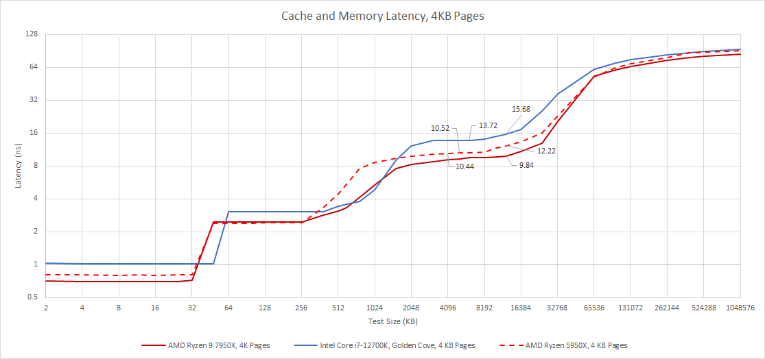
At the 12 MB test size and larger, we start to see Zen 4’s larger L2 TLB come into play. Zen 3 and Golden Cove both have to start doing page walks as accesses spill out of the L2 TLB, which potentially incurs up to 4 extra memory accesses to figure out the physical address. All three architectures have separate page directory caches in their page walkers that cache entries in higher level paging structures, so they’re probably not doing too many extra accesses at test sizes that barely spill out of the L2 TLB.
Still, even a fast page walk is worse than grabbing a translation straight out of the L2 TLB, so the difference is clear. Zen 3’s L3 latency rises above 12 ns at the 12 MB test size, while Zen 4 stays at just below 10 ns. Golden Cove suffers more, with latency exceeding 15 ns even though we’re still well within the 12700K’s 25 MB L3’s capacity.
So, AMD has done an impressive job of improving cache access latency, in ways that headline cycle count numbers don’t fully capture. Zen 4’s higher clock speeds mean that actual latencies for the L1 and L3 caches have improved, while the L2 cache gets its capacity doubled with an extremely minor latency regression (2.44 ns on the 7950X versus 2.4 ns on the 5950X). Improved TLB capacity further improves latency in practice, by reducing virtual to physical address translation overhead for typical applications. All of this comes together to give Zen 4 a significant latency advantage over Golden Cove at all cache levels.
Bandwidth, Single Core
While memory access latency is important, bandwidth can be important too. Vectorized code can be particularly hungry for memory bandwidth. Despite adding AVX-512 support, AMD has not made significant adjustments to core-private caches. Per-cycle load bandwidth remains similar to that of Zen 3 and Zen 2. Zen 4’s larger L2 is a welcome addition, because it should reduce bandwidth demands on the shared L3. But improvements in L1 and L2 bandwidth come down to Zen 4’s clock speed increase.
L3 bandwidth from a single core has improved on Zen 4, with an average of 27 bytes per cycle compared to 24 bytes per cycle on Zen 3. That’s quite close to the theoretical bandwidth of the interface from each core to L3. AMD has probably beefed up the size of the queue between L2 and L3, to the extent that it’s almost big enough to completely absorb L3 latency.

Intel has put a lot of emphasis on vector performance, and it shows. Golden Cove’s core-private caches can provide exceptional bandwidth, with the L1D handling three 256-bit loads per cycle, or two 512-bit loads per cycle. The latter is only possible with AVX-512, but Golden Cove holds a significant L1D bandwidth advantage even with AVX. This advantage persists in L2, where Intel has a 64 byte per cycle interface between L1D and L2. With AVX-512, Golden Cove has a staggering 40% bandwidth advantage over Zen 4, in L2 sized regions. AMD can’t achieve the same level of performance with AVX, because the L1D doesn’t have enough ports to handle a fill request from L2 and deliver full bandwidth to the core at the same time. Still, Golden Cove can still beat Zen 4 with just AVX.
The situation flips around in L3, where AMD’s excellent L3 design can deliver almost as much bandwidth as their L2. Intel’s bandwidth in contrast drops like a rock. Golden Cove barely averages 20 bytes per cycle from L3 with no contention from other cores.
When test sizes spill out into DRAM, Zen 4 maintains very high bandwidth per-core. This suggests each Zen 4 core is able to track a lot of pending L3 misses, or more specifically, L2 misses. AMD only fills its L3 cache with lines evicted from L2 (hence the term “victim cache”), which means it does not prefetch into L3. That makes Zen 4’s L2 the last cache level capable of generating prefetch requests. By being able to generate requests to L3 and beyond based on the access pattern it’s seeing from L1 misses, the L2 can utilize more available memory level parallelism at its level, without being limited by memory level parallelism generated by L1 misses.
We can even estimate the L2 miss queue size with Little’s Law:

Obviously this calculation isn’t perfect, because we tested with 4 KB pages out to very large test sizes, and didn’t make an attempt to estimate how often a page walk would result in requests to L3 and beyond. But it does suggest Zen 4 has more aggressive prefetching at L2, a deeper queue between L2 and L3, or both.
Multi-Threaded Bandwidth
With all threads loaded, Zen 4 achieves very high total bandwidth. That’s largely because it’s able to maintain a very high clock speed of over 4.8 GHz, judging by achieved L1D bandwidth. Because all levels of Zen 4’s cache hierarchy run at core clock, or at least at the speed of the fastest core in a cluster, the 7950X also enjoys increased L2 and L3 bandwidth even though the width of the buses between each cache level haven’t changed across Zen generations.

Intel’s Alder Lake is competitive against prior generations of AMD 16 core desktop CPUs. AMD had more “big” cores, but Golden Cove had wider buses to its L1D and L2 caches. But Zen 4’s higher clocks change that. Alder Lake can only match AMD’s L1D bandwidth if AVX-512 is in play, but that feature is of course not enabled. With or without AVX-512, Alder Lake can’t match Zen 4’s L2 bandwidth at all.
By splitting the L3 into clusters, AMD trades some cache capacity efficiency to make the bandwidth and latency problem easier to solve. For the past few Zen generations, AMD held a substantial L3 performance advantage over Intel. Zen 4 extends this further.
DRAM Bandwidth
Zen 4 also moves over to DDR5, which dramatically increases the memory subsystem’s theoretical bandwidth. We saw just above 50 GB/s of read bandwidth using a 5950X equipped with DDR4-3600, or just above 88% of theoretical DRAM bandwidth. Our DDR5-6000 equipped 7950X platform achieved 72.85 GB/s at the same 3 GB test size. On one hand, that’s a notable 43% increase in memory bandwidth. On the other, Zen 4 actually sees a decrease in memory bandwidth efficiency. A 128-bit DDR5-6000 bus can theoretically reach 96 GB/s, and we only achieved 76% of that.
One theory is that Zen 4’s DRAM bandwidth is limited by the link between the memory controller and fabric. AMD’s diagram shows that the link is 32 bytes per cycle wide in both directions.
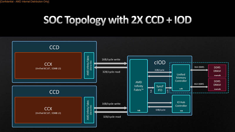
However, that is unlikely. FCLK in our testing was set to 2000 MHz. 32 bytes per cycle at 2000 MHz works out to 64 GB/s, which is well under what we were able to achieve. UCLK runs at 3000 MHz, or half of DDR transfer rate. 32 bytes per cycle at 3000 MHz should mean that full DDR bandwidth can be achieved in either direction. That does not rule out a bandwidth limitation at the link between Infinity Fabric and the memory controller, but it does suggest the link to fabric is wider than AMD’s diagram suggests.
Another related theory is that bandwidth can be improved if we mix reads and writes in a 1:1 ratio, since the link can deliver 32 bytes in each direction. However, mixing reads and writes introduces a different problem at the DRAM level. Unlike links to cache, the DRAM bus is not bidirectional and has to be explicitly switched between read and write modes. These switches are not free and force the memory bus to idle for a number of cycles, reducing achieved bandwidth. Therefore, we don’t see a significant bandwidth increase when using an access pattern that mixes reads and writes.
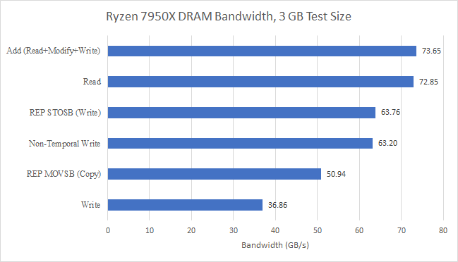
With a read-modify-write access pattern, we see a 1% bandwidth increase, which is hardly even worth talking about. The write pattern is actually a 1:1 mix of reads and writes too, since each write operation (except in special cases) requires a cacheline to be read as well. That’s because the instruction might only modify part of the cacheline, and the CPU needs to merge the write with the existing cacheline contents. That read is known as a “read for ownership”, or a RFO, because it means the reading core owns the cacheline and has a guarantee that no one else can write to it. If we account for that by multiplying 36.86 GB/s of write bandwidth by two, we get 73.72 GB/s, which is again not very different from pure read bandwidth.
Other access patterns see significant drops, including the copy pattern with REP MOVSB. That test uses a microcoded string copy instruction that tells the CPU exactly how much data it needs to move, which lets it avoid RFOs. It therefore also features a 1:1 mix of reads and writes.
We do see some evidence that write bandwidth might be limited by the links between the CCDs and the IO die. AMD’s diagram shows that those links are 16 bytes per cycle wide. Across both CCDs, that works out to 64 GB/s at 2000 MHz FCLK. With special write instructions that avoid RFOs, we get extremely close to 64 GB/s, but not more. The REP STOSB instruction tells the CPU upfront how much data to set to a particular value, letting it avoid RFOs when it knows an entire cacheline will be overwritten. Non-temporal writes (with MOVNTPS) use a write-combining memory protocol that also avoids RFOs, and bypasses caches. Both methods reach within 1% of theoretical CCD to IO die write bandwidth. This is unlikely to be a limitation in most applications, where memory reads far outnumber memory writes.
As far as Zen 4’s read memory bandwidth goes, a fabric bandwidth limitation is unlikely. Instead, the new DDR5 memory controller seems to be less efficient than the old DDR4 one at extracting every last bit of bandwidth. Maybe it’s not scheduling requests as well and runs into secondary timings more. But the big picture is that Zen 4 enjoys a significant bandwidth advantage over prior Zen generations, thanks to DDR5 memory. AMD’s 16 core desktop Ryzen chips can become memory bandwidth bound, if given well threaded, vectorized loads. Even with reasonable cache hitrates, 16 cores can draw a lot of bandwidth, so DDR5’s bandwidth boost is appreciated. And even DDR5 bandwidth won’t be enough to feed 16 cores, so AMD continues to rely on effective caching to maintain a performance edge in well-threaded workloads.
Conclusion
As its name suggests, Zen 4 is the fourth installment in AMD’s line of Zen architectures. Like Zen 2, Zen 4 combines an architectural change with an improved process node to deliver a generational performance increase. At the same time, AMD reduces risk by avoiding more drastic changes while attempting to transition to a new process node. So, it’s not a surprise to see similar changes in a lot of areas, particularly with caching and register files, where improved density makes larger capacities feasible.

However, Zen 4 does skip out on some areas, especially where vector execution is concerned. Compared to Zen 3, and even Zen 2, Zen 4 does not increase native vector execution width, and does not boost maximum L1D bandwidth. Zen 2 also made minor execution and scheduling changes over Zen 1, while Zen 4 keeps Zen 3’s configuration. The result is a claimed 13% IPC increase. Compared to the last two Zen generations, this might seem underwhelming. But 13% is comparable to the jump between Ivy Bridge and Haswell, which Anandtech puts at 11.2%. We also have to take performance per clock increases with clock speed in context.
Performance increases are never about IPC increases alone, because clock speed matters as well. Performance generally scales almost linearly with clock speed increases, provided your caches are doing well enough to keep DRAM bottlenecks away. If you have a choice between increasing some structure sizes by 5%, or being able to clock the core 5% higher, you’re almost guaranteed to get higher overall performance by picking the latter option. AMD’s engineers probably avoided beefing up certain structures, like the schedulers and store queue, in favor of getting the core to clock higher. And Zen 4 did clock higher, by a large margin. The end result is an overall performance improvement that should be in line with what we got from previous Zen generations. Zen 4 carries this clock speed advantage to multithreaded workloads. Every Zen generation delivered strong all-core performance, and Zen 4 is no exception. Intel also pursued a similar strategy with Raptor Lake, which avoided major architectural changes. Instead, maximum clocks were pushed to 5.8 GHz with Thermal Velocity Boost, or 5.7 GHz with regular Turbo Boost 3.0.
Averaging IPC across a large set of workloads also obscures Zen 4’s AVX-512 advantage. Programs that use AVX-512 can get the same amount of work done with fewer instructions, thus achieving lower IPC, but higher performance per clock. I assume when AMD says IPC, they mean performance per clock, not specifically instructions per clock. In specific workloads that can take advantage of AVX-512, I expect Zen 4 to pull a large advantage over Zen 3. If 512-bit vectors are used, Zen 4 will have more effective scheduling capacity even though the size of the scheduler queue stays the same, because each scheduler entry will be tracking 512 bits worth of work. Even if longer vectors aren’t used, AVX-512 offers new instructions that again let the CPU get the same amount of work done with fewer instructions.
Other Zen 4 changes similarly focus on making better use of existing execution capacity. Raw execution throughput per cycle hasn’t really changed from Zen 2 to Zen 4, and cache bandwidth hasn’t increased either. That’s because AMD already had plenty of raw throughput in prior generations, and steady state execution throughput wasn’t a bottleneck in most applications.

Zen 4 therefore improves reordering capacity to help absorb bursts of demand for the execution units. Improved branch prediction helps better utilize both reordering capacity and execution unit throughput, by reducing wasted work. Zen 4 also tries to feed the execution units better by switching to DDR5, which provides a large bandwidth boost over DDR4. At the same time, AMD has given each core more memory level parallelism capabilities. The amount of DRAM bandwidth achievable with a single core to increases to over 57 GB/s, indicating very deep buffers to track pending cache misses. These deep buffers help absorb spikes in demand for cache and memory bandwidth. From the other direction, Zen 4’s larger L2 TLB and L2 cache help reduce average latency for instructions that access memory. Intel has pursued a similar strategy in Raptor Lake, where P-core L2 size was increased from 1.25 MB to 2 MB at the cost of just one cycle of latency.
Zen 4 also aims to improve frontend width utilization instead of making everything wider. Zen 3 already had a very fast branch predictor, but Zen 4 takes it further. A bigger L1 BTB with a higher hitrate means the frontend spends fewer cycles idling after a taken branch, increasing frontend width utilization. Like prior Zen generations and many Intel architectures, Zen 4 is narrowest at the renamer, which remains 6-wide. I’m guessing AMD found they could improve performance more by increasing clocks than boosting core width. The renamer is probably a very timing sensitive bit of circuitry. Each instruction coming in could require two or more reads from the register alias tables, and modifications to register mappings have to be reflected immediately, for later instructions coming in within the same 6-wide group.

With all that in mind, I wonder how much AMD can squeeze out of a certain core width and set of execution resources. Some areas of the Zen 4 core look very light in comparison to competing Intel cores. For example, L1D bandwidth for vector loads and stores is only half of what Intel can achieve with AVX-512. Even when limited to 256-bit accesses with AVX, Golden Cove can still achieve more bandwidth per cycle than Zen 4. Of course, Intel can’t pack 16 Golden Cove cores into a chip and run them all at high clocks. Also, Intel managed to increase IPC by ridiculous amounts between Conroe and Skylake, even though both architectures (and everything in between) were 4-wide. I look forward to seeing what AMD and Intel both bring in future generations.
If you like our articles and journalism and you want to support us in our endeavors then consider heading over to our Patreon or our PayPal if you want to toss a few bucks our way or if you would like to talk with the Chips and Cheese staff and the people behind the scenes then consider joining our Discord.