
Skylake: Intel’s Longest Serving Architecture

Intel debuted Skylake in 2015. Then Skylake variants filled out major parts of Intel’s lineup for the next six years. Skylake faced no serious competition at launch, but wound up holding the line against three generations of AMD’s Zen CPUs while Intel struggled to roll out a new architecture across its lineup. Technically, Rocket Lake replaced Skylake-derived Comet Lake CPUs in 2021, but Comet Lake retained a compelling place in Intel’s lineup because Rocket Lake failed to beat it in gaming performance and core count. Skylake wasn’t superseded across all of Intel’s lineup until Alder Lake’s launch in late 2021, making it the longest serving Intel architecture in recent memory.

Yet Skylake is an odd architecture to hold the line for so long with, because it makes a relatively small leap over Haswell in terms of client performance. Sandy Bridge and Haswell both brought large improvements over previous generations, and these improvements largely applied across both client and enterprise applications. Intel definitely made some major changes to create Skylake, but these were mostly geared towards the server market, or were blunted by lack of changes elsewhere.
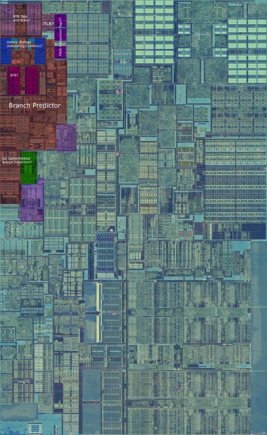
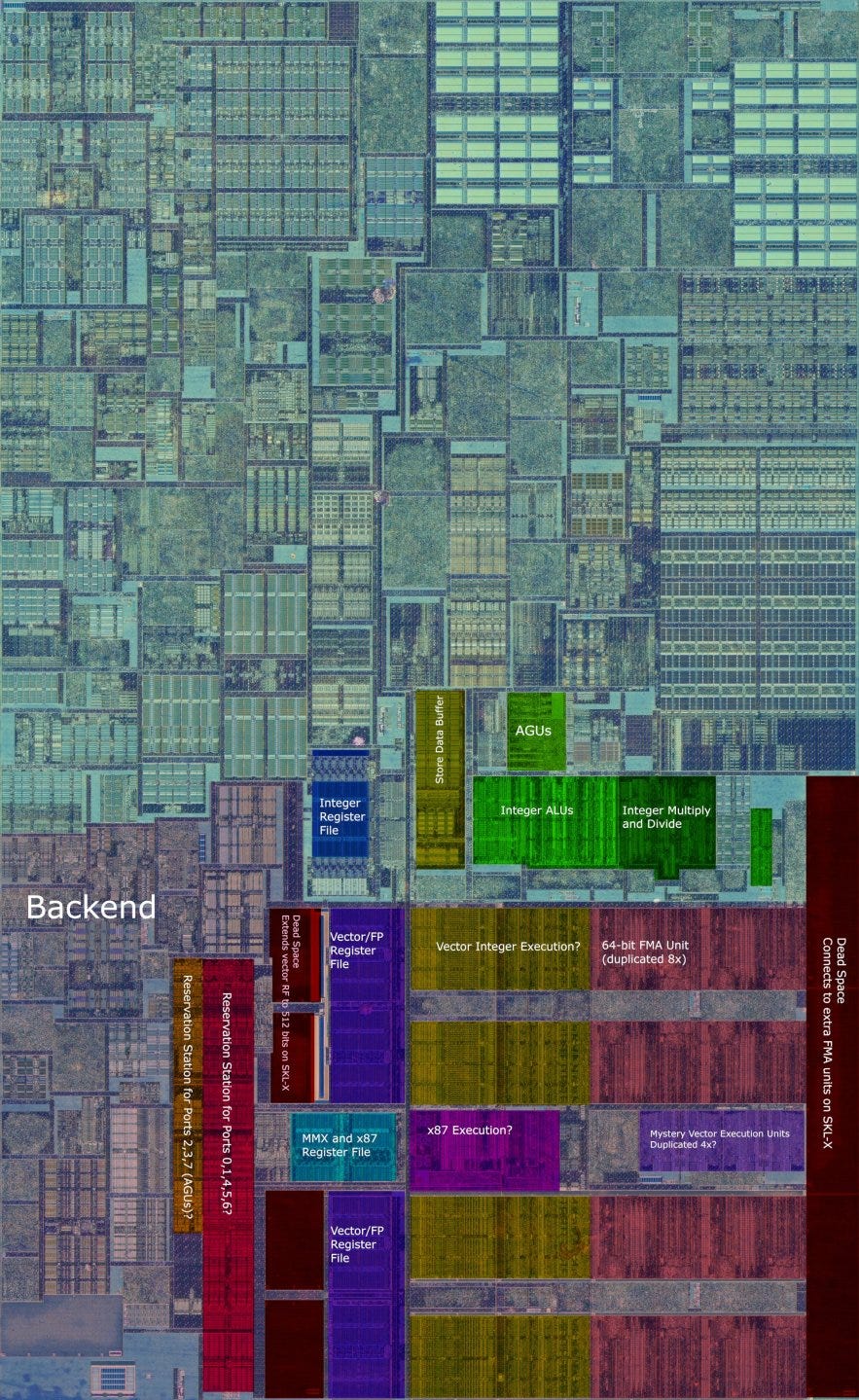
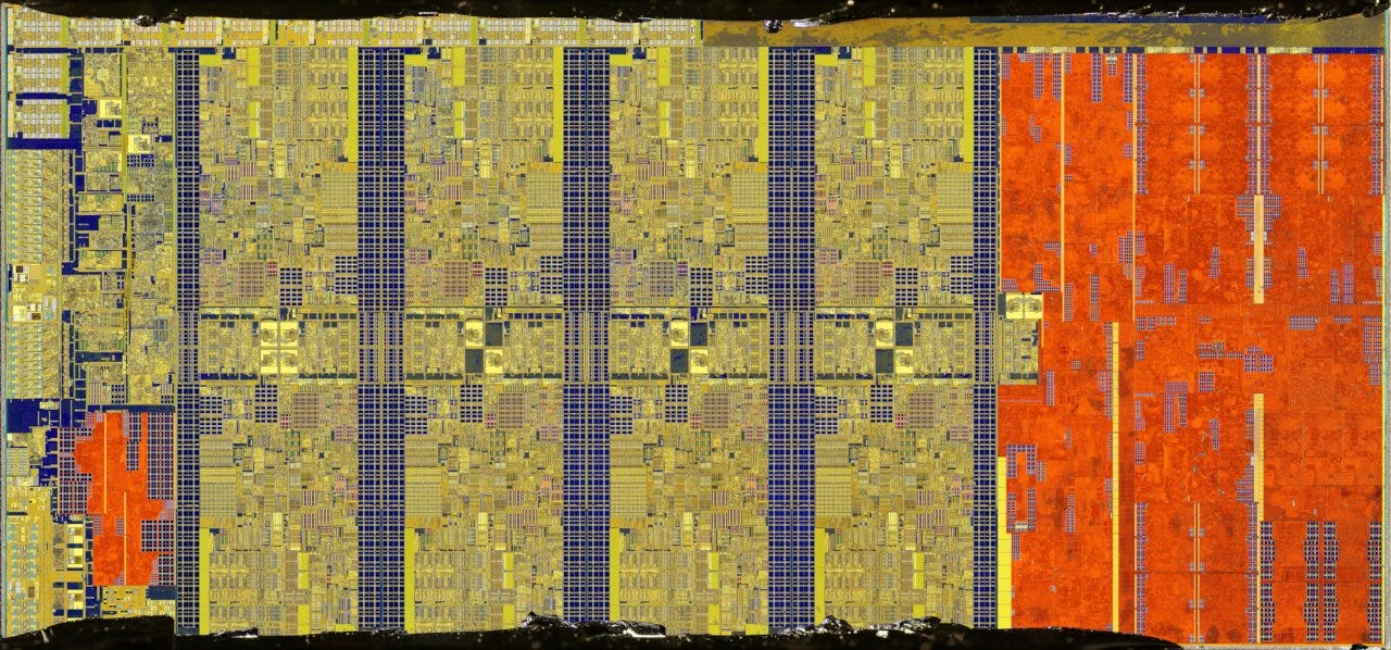
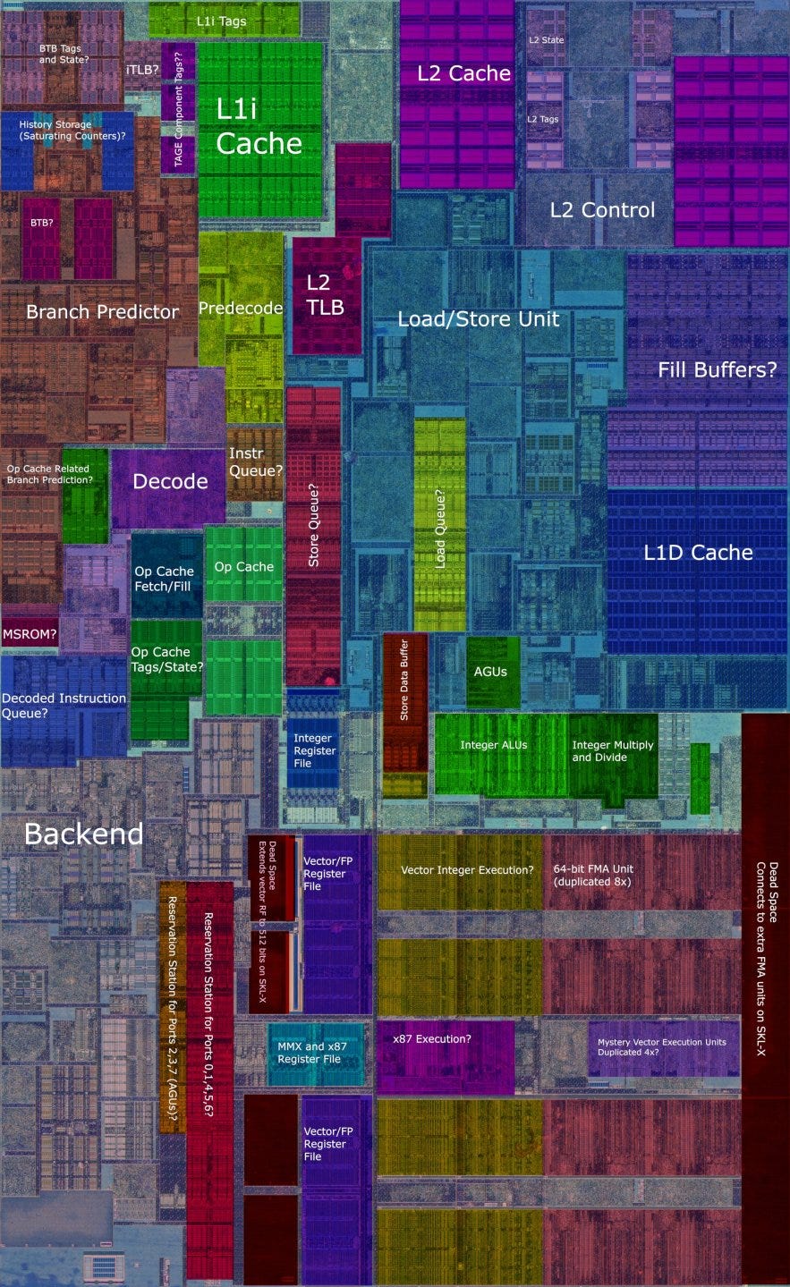
Block Diagram
Skylake represents an evolution over Haswell. Haswell was already a very strong architecture that faced no serious competition throughout its life. The Haswell core is well balanced with few weaknesses and very strong vector execution. Skylake builds on this foundation and makes it a bit better.
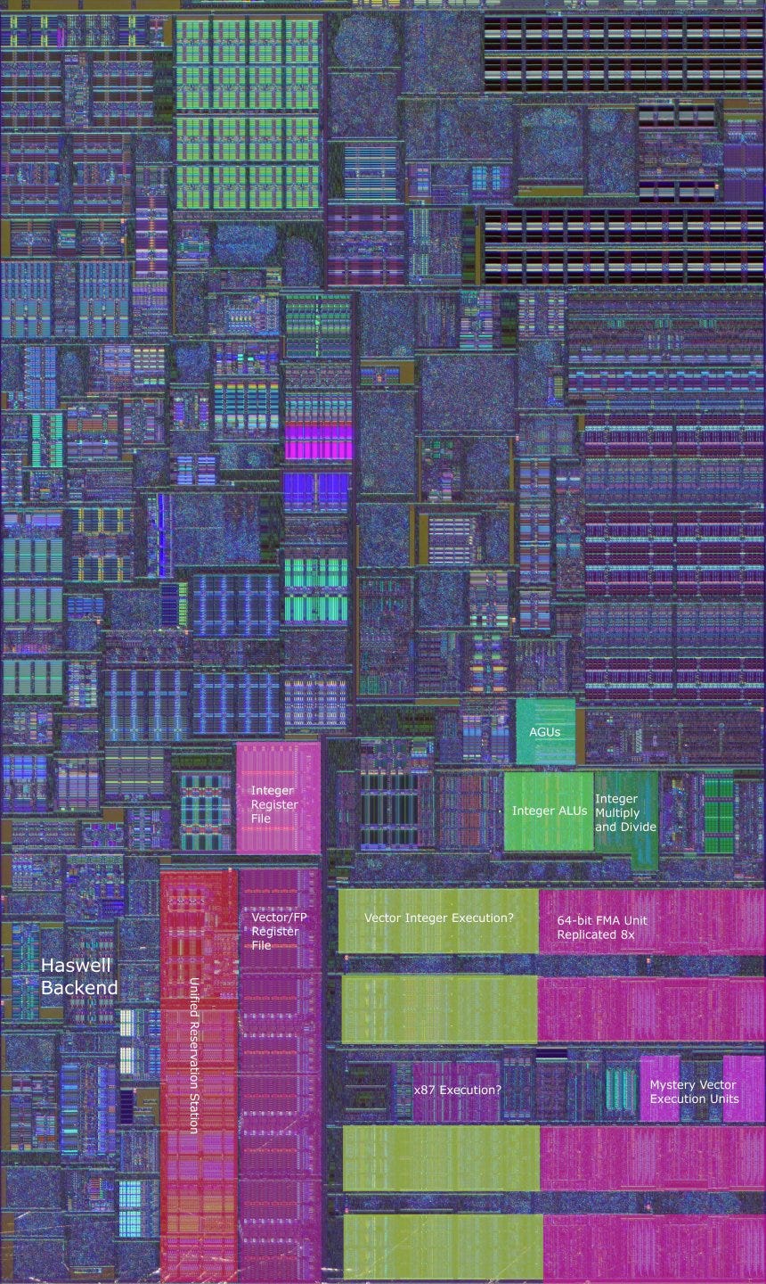
For comparison, here’s Haswell:
Frontend: Branch Predictor
A CPU’s branch predictor is responsible for accurately and quickly generating instruction fetch addresses. Because the branch predictor can have a large impact on performance, engineers typically tweak it with every generation. Skylake’s branch predictor behaves a lot like Haswell’s. That’s not necessarily a bad thing, because Haswell already had the best branch predictor around in the mid 2010s. AMD’s Piledriver was the only real desktop alternative, and was a pretty big step behind. Skylake therefore continued Intel’s tradition of having a class leading branch predictor when it launched in 2015.

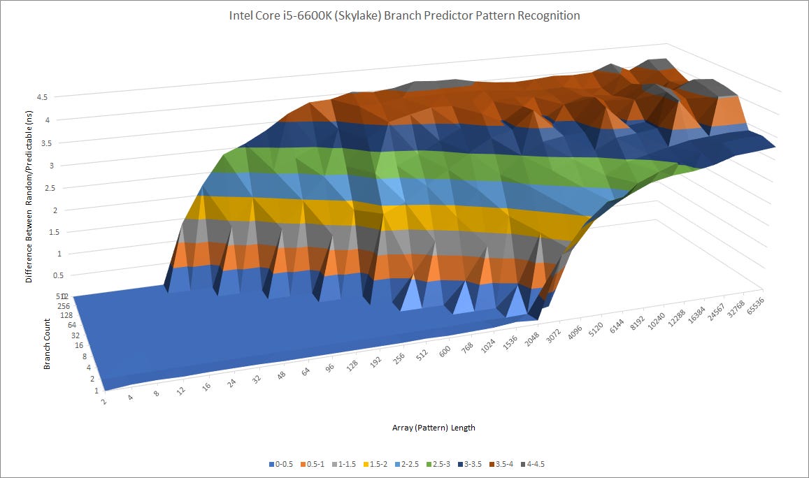
Intel might have changed the direction predictor in ways that aren’t so straightforward to detect. But if they did, we’re not seeing much of an impact from a quick look at achieved branch prediction accuracy:

Speed is the other component of branch predictor performance. A slow predictor can force the frontend to stall for a lot of cycles and possibly starve the execution engine of instructions. Like Haswell, Skylake has a two level cache of branch targets (the BTB). The first level can track up to 128 branch targets and handle them with no wasted cycles after a taken branch. The second level tracks 4096 branch targets, and costs one penalty cycle if a branch target comes from it.
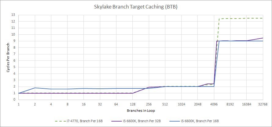
Skylake displays faster branch handling when BTB capacity is exceeded, hinting at a faster branch address calculator, or a branch address calculator located earlier in the pipeline. However, it slightly regresses compared to Haswell with dense branches. Haswell could handle up to 128 branches with no penalty if they’re spaced by at least 16 bytes, but Skylake requires them to be spaced by 32 bytes.
One significant improvement is with return handling if call depth exceeds return stack capacity. Skylake can fall back on its indirect predictor in this case, resulting in reduced penalties if the predictor guesses correctly.
Frontend: Instruction Fetch
Once the branch predictor has generated fetch addresses, the frontend has to go get the instructions and provide decoded micro-ops to the renamer. Skylake’s instruction fetch and decode setup is wider and deeper than Haswell’s. The instruction byte buffer between the L1i cache and decoders grows from 20 entries per thread on Haswell to 25 on Skylake. Skylake also has a larger decoded instruction queue placed in front of the renamer, with 64 entries per thread. Haswell has 56 entries in its decoded instruction queue, and gives each thread 28 entries when both SMT threads are active. This increased buffering capacity helps Skylake smooth out spikes for demand in instruction bandwidth a little better than Haswell can. Intel also increased the instruction TLB’s associativity, which should improve hitrates and cut down virtual to physical address translation penalties.
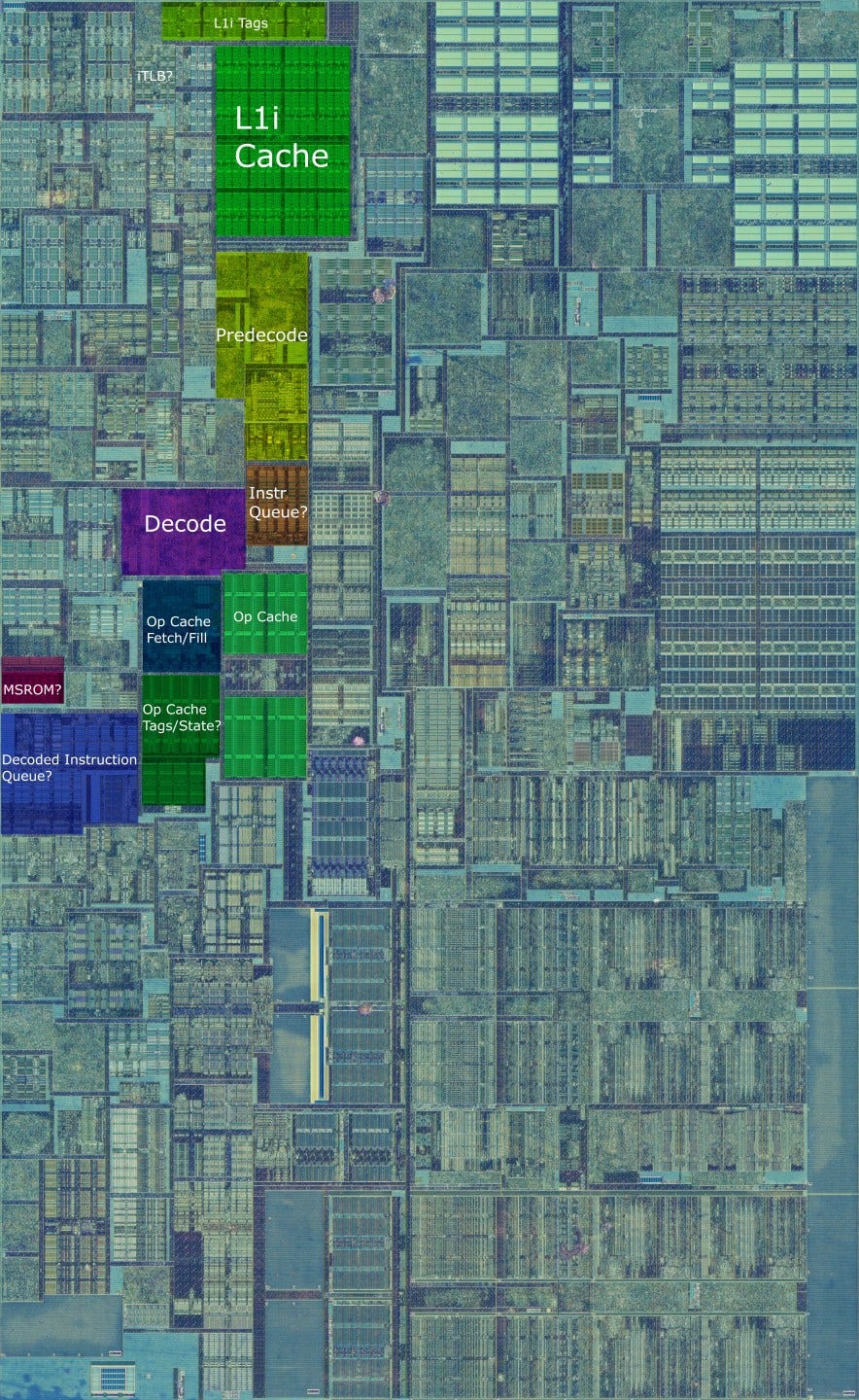
Skylake also gets improved decoders capable of emitting 5 micro-ops per cycle. However, the decode unit can only handle 4 instructions per cycle, so you can only get 5 micro-ops out of the decoders when one of the instructions decodes into two or more micro-ops. Most instructions decode into a single micro-op on Skylake, including ones that combine a memory and ALU operation. The extra bandwidth from the decoders is therefore unlikely to have a large impact.
Intel also increased the micro-op cache’s bandwidth. It can now fetch 6 micro-ops per cycle, up from four on Haswell. Intel’s micro-op cache has stored micro-ops in lines of six since Sandy Bridge, so fetching an entire line of micro-ops at once makes a lot of sense. This effectively makes the frontend 6-wide, though its effect on performance is blunted because the rename stage afterward is only 4-wide.
Skylake and Haswell therefore have similar instruction bandwidth when code footprints fit within the micro-op cache or L1i, because Skylake’s frontend is bottlenecked by the renamer. However, Skylake has a nice bandwidth advantage when pulling code from L2 or beyond. Intel likely gave Skylake more memory level parallelism capabilities and more aggressive prefetch on the instruction side.

If we swap over to 4 byte NOPs, which are more representative of instruction lengths encountered in integer code, Skylake can get relatively high instruction bandwidth from any level of cache. Even when fetching code from L3, Skylake can maintain almost 3.5 IPC, which isn’t far off from the core’s width.

Haswell also does quite well in this test, and maintains respectable instruction side bandwidth when it has to fetch code from L2 or L3. 2.2 to 2.5 IPC is still nothing to sneeze at, and should be enough to feed the backend especially when it’s choking on cache and memory latency. Both Intel CPUs are well ahead of AMD’s Piledriver, which can barely fetch more than 4 bytes per cycle when pulling code from L2.
Rename and Allocate
The rename stage serves as a bridge between the in-order frontend and out of order backend. Skylake’s renamer is 4 wide, just like Haswell’s. Both cores can recognize common zeroing idioms, and eliminate register to register copies.

Performance counters also show Skylake eliminating the XOR r,r and SUB r,r zeroing idioms at the renamer, without sending any micro-ops down to the ALU ports. That’s not a particularly big deal for Skylake, since it has four ALUs and thus plenty of ALU throughput. For comparison, Piledriver can break dependencies between zeroing idioms, but doesn’t eliminate them. AMD has to use ALU ports to set registers to zero, which increases pressure on its two ALUs.
Backend: Out of Order Resources
To avoid getting stuck on long latency instructions, CPUs use out of order execution to move past them in search of independent instructions that can keep the execution units busy. Deeper buffers allow the CPU to move further ahead before the pipeline backs up. As is tradition with every Intel microarchitecture update, Skylake gets a bigger backend with more reordering capacity.

Entries in the scheduler, integer register file, and store queue are often in high demand, so all of those structures got a boost. Intel paid particular attention to the scheduler, giving it a massive increase in entry count. To pull this off, they ditched one of the last remaining bits of DNA left from P6 by getting rid of the unified scheduler. Unified schedulers can flexibly allocate their entries among ports attached to it and take fewer total entries to reach a certain performance level than a distributed scheduler. But multi-ported structures are generally very expensive, and an octa-ported unified scheduler with 97 entries was probably too much. So, Intel split the scheduler into two parts. A 58 entry scheduler serves Skylake’s four math ports and the store data port, while a separate 39 entry scheduler handles the three AGU ports.
While not completely unified, Skylake’s scheduler is still more unified than the schedulers we see on AMD’s Zen lineup, at least if we look at the integer side. Each of Skylake’s schedulers still has a lot of entries serving a lot of ports. Since Sandy Bridge, Intel’s big core architectures have become more and more unrecognizable as P6 descendants, and Skylake takes yet another step in that direction.
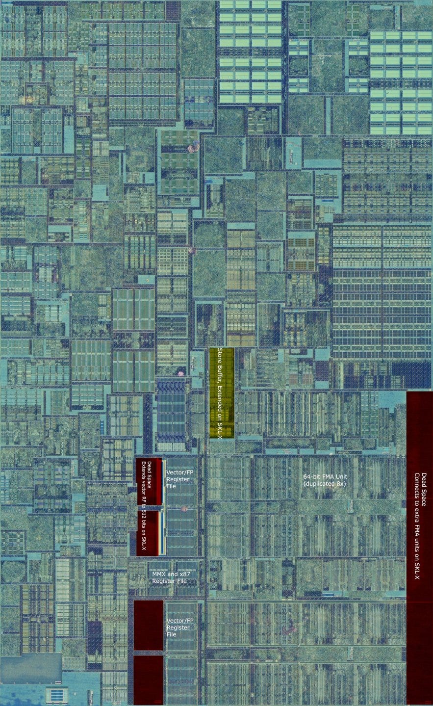
Skylake’s register file layout also received major changes, though the picture is more complicated here. Intel made a major move by adding a separate physical register file to hold results from MMX and x87 instructions. Prior Intel CPUs used a single vector register file to handle renaming for both x87/MMX registers and SSE/AVX ones. At first, Skylake’s change makes little sense. SSE (and its later extensions) were meant to replace x87 and MMX, so there’s not a lot of vector/FP heavy programs out there mixing MMX/x87 and SSE/AVX instructions.

The new register file does improve reordering capacity for SSE/AVX registers because MMX/x87 state doesn’t have to be stored in the main 256-bit vector register file. But such an improvement could have been accomplished in a far more straightforward manner by simply adding entries to the vector register file. Client Skylake has a chunk of unused die area next to the vector register file, so there’s certainly space available to employ that strategy.
To understand why Intel made such a major change that doesn’t have a tangible effect on client performance, we have to look at server Skylake and AVX-512. There, the new register file also serves as the mask register for avx-512. Masking is a new feature in AVX-512 that lets code “mask off” lanes, a bit like how GPUs handle branching. Having a separate register file for mask registers makes a lot of sense for AVX-512 code, as it would prevent mask register writes from competing with regular integer instructions for register file capacity. Unfortunately, client Skylake doesn’t support AVX-512, so the extra register file represents a lot of wasted engineering effort and die area from the client perspective.
Overall, Skylake’s larger out-of-order execution buffers mean that it’s a bit less backend bound than Haswell:
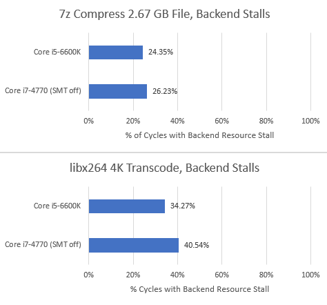
The decrease in resource stalls is pretty small, but that’s to be expected. Increases in reordering capacity run into diminishing returns, and Skylake doesn’t make massive structure size increases like Sunny Cove did.
Backend: Execution Units
Client Skylake’s port layout is similar to Haswell’s. There are four integer execution ports, two general purpose AGU ports, and a store-only AGU port. Three of the integer execution ports, numbered 0, 1, and 5, handle floating point and vector execution as well.

Even though port layout wasn’t changed, Intel did beef up floating point and vector execution capabilities. On the floating point side, latency for floating point adds, multiplies, and fused multiply adds are all standardized at four cycles and two per cycle throughput, suggesting the fused multiply add (FMA) units are handling all of those operations. Haswell could see pressure on port 1 if code had a lot of FP adds, but couldn’t take advantage of FMA. Skylake fixes this by letting FP addition work on both port 0 and port 1.

Intel added more vector execution units too, again reducing pressure on certain ports. Vector integer multipliers got duplicated across ports 0 and 1. Ports 0, 1, and 5 can all handle vector integer addition. Bitwise operations on floating point types (i.e., vorps) can execute on all three vector execution ports, while Haswell could only handle them on port 5. Skylake should therefore be a tad stronger than Haswell when dealing with vectorized workloads.
Backend: Load/Store Execution
Any pipelined CPU faces the annoying task of figuring out whether a load should get data from the memory subsystem, or have data forwarded to it from an in-flight store ahead of it. Skylake handles store to load forwarding a lot like Haswell, but there are small improvements. While Haswell takes 5-6 cycles to forward a store’s data to a later load, Skylake can almost always do so in 5 cycles. Rarely, Skylake is able to forward data in less than 5 cycles if the store and load’s addresses match exactly.

Otherwise, there’s not much difference between Haswell and Skylake. Both seem to do a quick initial check to see if stores and loads access the same 4 byte region, and often take an extra cycle to do a more thorough check if they do. Store forwarding only fails if the load only partially overlaps with a store. In that case, latency increases to 15 cycles.

On both architectures, stores crossing a 64 byte cacheline take two cycles to complete. Loads that cross a cacheline boundary can often complete in a single cycle, likely because the L1 data cache has two load ports. Haswell and Skylake’s load/store units are both massively superior to Piledriver’s. Piledriver takes around three more cycles to forward store results, and more crucially, can’t forward results to partially overlapping loads when crossing a 16 byte boundry. Failed store forwarding penalties are generally higher on Piledriver as well.

AMD also suffers from more misaligned access penalties, since those happen when crossing 16 byte boundries instead of 64 byte ones like on Intel.
But one area where AMD does have an advantage is Meltdown vulnerability. AMD’s architectures don’t wake up instructions dependent on a faulting load, making them invulnerable to Meltdown. Intel CPUs however seem to check whether a load result is valid at a later pipeline stage, allowing a faulting load to cause speculative side effects (like getting a certain cacheline loaded into L1D). Skylake is vulnerable to this as well, but Intel introduced a mitigation with the Whiskey Lake variant. On Whiskey Lake and subsequent Skylake variants, a faulting load’s result will always be zero. While this isn’t as watertight as not producing a load result at all, it does reduce the attack surface for Meltdown.
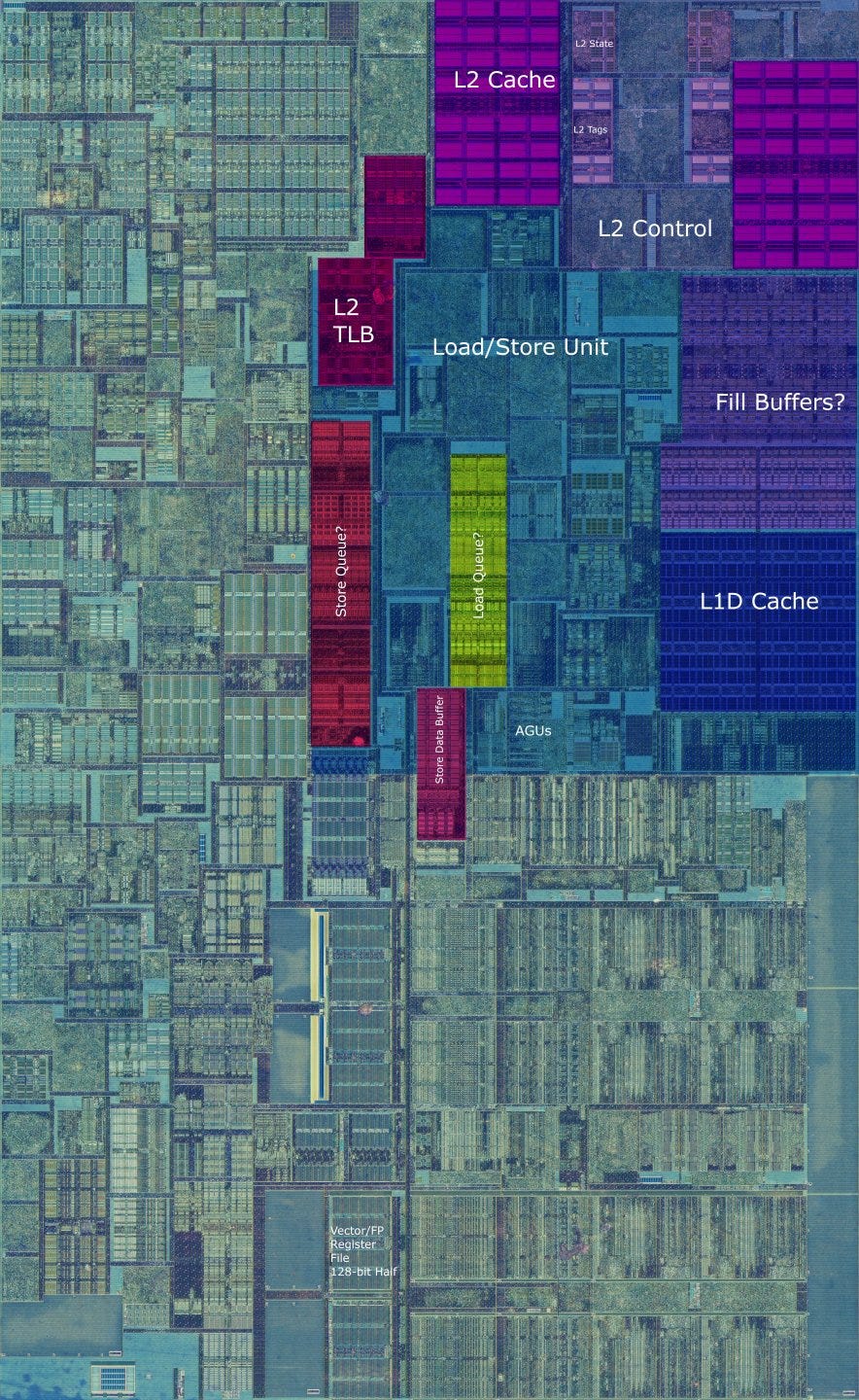
Cache and Memory Access
Skylake’s memory hierarchy is almost identical to Haswell’s, at least on client implementations. Intel found a winning formula with Sandy Bridge’s triple level cache hierarchy. Cores get a 32 KB L1 data cache and a modestly sized 256 KB L2 cache to insulate them from L3 latency. The L3 is constructed with slices distributed across the ring bus with one slice per core, effectively giving the L3 as many banks as there are cores and allowing bandwidth to scale with increasing core count.
In terms of cache geometry, Skylake decreases the L2 cache’s associativity from 8-way to 4 way. This was likely done to allow expanding the L2 cache’s capacity in Skylake X by adding more cache ways. Expanding a 256 KB 8-way L2 to 1 MB by adding more ways would have resulted in a ridiculous 32-way associative cache, so Intel made a small sacrifice on the client side to allow a different server configuration.
Latency
As far as cache latency goes, the only notable change from Skylake to Haswell is a gentler curve up to L3 latency as L2 capacity is exceeded, hinting at a different L2 cache replacement policy. At Skylake’s launch, that’s not a bad thing because Intel had a class leading cache hierarchy. Latencies in an absolute sense are very good. L3 latency is under 10 ns, while L2 latency is just above 3 ns. AMD’s Piledriver also has a triple level cache hierarchy, but each level of cache is much slower than Intel’s.

Piledriver does have a small window between 256 KB and 2 MB where its L2 cache can provide data at lower latency than Intel’s L3. But CPUs have to translate virtual addresses to physical ones before going to their L2 and L3 caches. Switching over to 4 KB pages, we can see that Piledriver takes quite a bit of additional latency when loading translations from its L2 TLB. Adding L2 TLB and L2 cache latency puts Piledriver only slightly ahead in that 256 KB to 2 MB region.

To improve average address translation latency, Skylake increases L2 TLB size from 1024 entries on Haswell to 1536 on Skylake. Associativity for the L2 TLB drops from 8 way to 6 way (at least as reported by cpuid), which helps keep L2 TLB latency and power draw under control.

Skylake’s L2 TLB size increase is more than enough to make up for the reduced associativity, and we see a drop in L2 TLB misses.
Bandwidth
For its time, Haswell was a bandwidth monster for any code that could utilize 256-bit AVX instructions. Skylake carries on that tradition, and makes slight improvements to cache bandwidth beyond L2. Most likely, this is because Intel increased the size of the queue between L2 and L3 from 16 entries to 32 entries. This allows more memory level parallelism from L3, letting a core better hide L3 latency and get improved bandwidth from L3 (and DRAM).

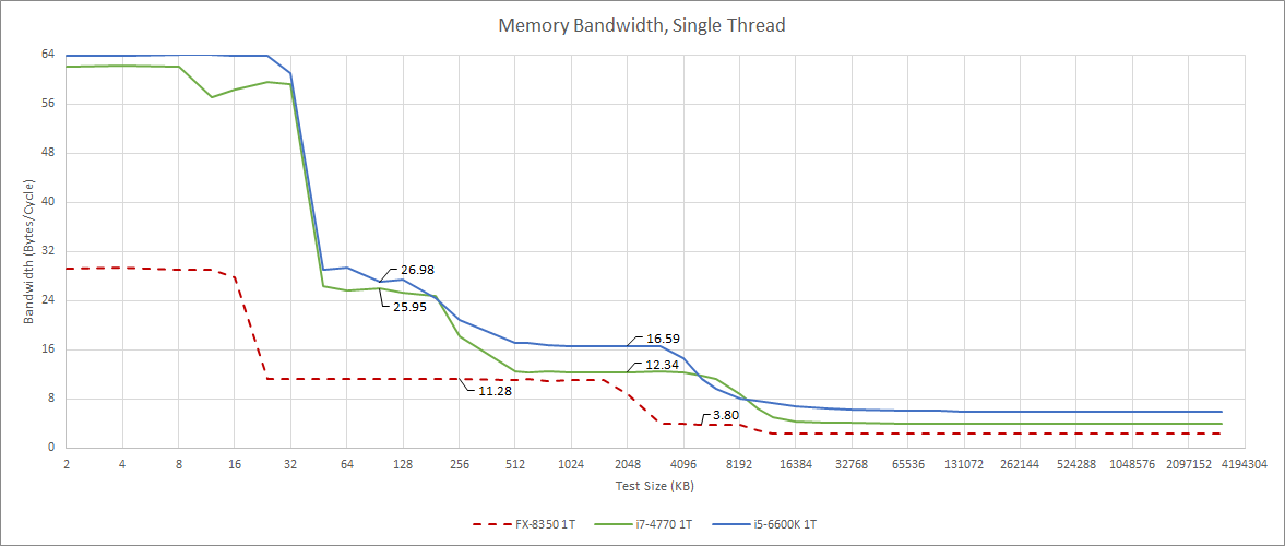
Piledriver was far behind Haswell, and of course remains behind Skylake. A single thread on Piledriver can’t even pull more bandwidth from L2 than Haswell or Skylake can from L3. Multi-threaded bandwidth paints a similar picture.

Again, Haswell and Skylake enjoy superior bandwidth at every level in the cache hierarchy. However, Piledriver does take a small lead if thread-private data fits within its larger 2 MB L2 caches, but doesn’t fit within Skylake or Haswell’s 256 KB L2. Core-private caches are easier to optimize for low latency and high bandwidth than shared ones, and AMD took advantage of that. Compared to the Intel chips, Piledriver has plenty of total cache capacity because its L3 isn’t inclusive of L2 contents. But Piledriver’s L3 bandwidth is again disappointing at just under 40 GB/s. Haswell and Skylake both achieve several times more bandwidth from their L3 caches.
Server Skylake (Skylake-X)
Up to Haswell, Intel used the same core architecture across server and client SKUs. Skylake largely uses the same architecture on server as well, but makes a few significant modifications. All of these changes work together to improve Skylake-X’s vector and multithreaded performance. We’ll go through these in no particular order, starting with the cache setup.
Server Skylake switches from using a ring based network-on-chip to one based on a mesh. A mesh allows more cores and cache slices to be connected and reach each other with lower average hop counts than with a ring. Using a mesh, Intel was able place 28 cores on a monolithic die, massively increasing per-socket multithreaded performance compared to Haswell, which only scaled up to 18 cores.

Theoretically, this sounds great. But in practice, a mesh’s advantage in lowering hop count seems to be offset by needing to run the mesh at lower clock speeds. That could be because a single node in a ring setup only needs two connections, while a mesh node can connect to four adjacent neighbors. In any case, Skylake-X’s mesh based L3 suffers from much higher latency. Bandwidth from L3 is lower as well:

Skylake-X therefore gets a much larger 1 MB L2 cache to insulate it from the slower L3. These changes make sense for multithreaded performance as well. As mentioned before, it’s much easier to scale bandwidth for core-private caches, so Skylake-X’s strategy for high multithreaded performance is to keep as much data in L2 as possible. Feeding the cores from L2 also makes sense for vector performance. AVX-512 support makes Skylake-X cores more bandwidth hungry than their client cousins, and a high bandwidth L2 is better suited to satisfy those bandwidth demands than a shared L3. This is especially the case for Skylake-X, which can deliver very high bandwidth from its L2 cache with AVX-512.
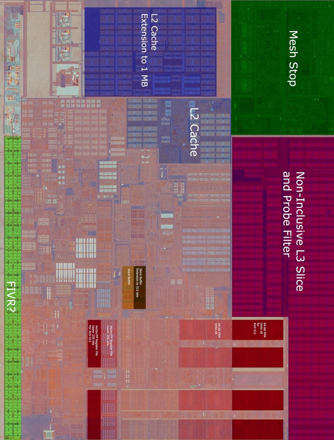
Those cache changes mean the L3 plays a less important role. In a sign of Intel’s future strategy, Skylake-X also makes the L3 non-inclusive. With the L2 size increase, an inclusive L3 would use most of its capacity duplicating L2 contents.
AVX-512 also brings a set of changes within the core. The L1 data cache can handle two 512-bit loads and a 512-bit store every cycle, doubling bandwidth compared to client Skylake. With AVX-512 code, Skylake-X enjoys massive L1 bandwidth, even though it typically runs at lower clocks than client Skylake.
Intel’s diverged approach to client and server SKUs makes sense, considering client and server workloads have different priorities. A cache setup that emphasizes multithreaded performance scaling makes sense with server workloads, which scale to higher core counts than client applications. First class AVX-512 support makes sense for HPC applications, which are quick to take advantage of new instruction set extensions. However, client Skylake made sacrifices to enable this flexibility:

Reviewers like Anandtech pointed out that Skylake delivered a minor 5.7% performance per clock increase over Haswell, which is quite small compared to Haswell’s 11.2% boost over Ivy Bridge. I feel like Intel could have delivered a performance boost closer to 10% if they focused completely on optimizing Skylake for client workloads. But that wasn’t a priority for them.
Skylake Soldiers On
So far, we’ve been mostly comparing Skylake with its desktop competitors at launch, namely Haswell and AMD’s Piledriver. But as the years went on, Skylake found itself competing on a changing landscape with increasingly tough competition from AMD. Zen 1 launched in 2017 with desktop SKUs that provided up to eight cores, giving it clear multithreaded performance advantage over quad core client Skylake parts. Zen 1’s per-core performance wasn’t a match for Skylake’s, but the gap was much smaller. In 2019, Zen 2 doubled core count again while making significant gains in per-core performance.
To keep Skylake in the game, Intel made improvements on multiple fronts. 14 nm process tweaks extended the power/performance curve, while improving performance at lower power targets. That strategy generally succeeded in keeping per-core performance competitive against AMD’s.

Intel also took advantage of their modular design to implement more cores and L3 cache slices. While this mainly served to counter Zen’s jump in multithreaded performance, the increased L3 capacity helped low threaded workloads too. Against Zen 1, this worked fairly well. Higher clock speeds and better performance per clock meant each Skylake-derived core generally punched harder than a Zen 1 core, so Intel wasn’t as far behind for well threaded applications as core count alone would suggest.
L3 cache latency increases by around 11 cycles when going from four core/L3 ring stops to ten, bringing actual latency from 8-9 ns to just over 10 ns. Latency is therefore still very reasonable, especially for a cache that’s twice the size serving twice as many cores. Intel’s strong ring bus architecture and modular design deserves a lot of credit for allowing Intel to keep pushing Skylake while their 10nm efforts hit repeated delays.

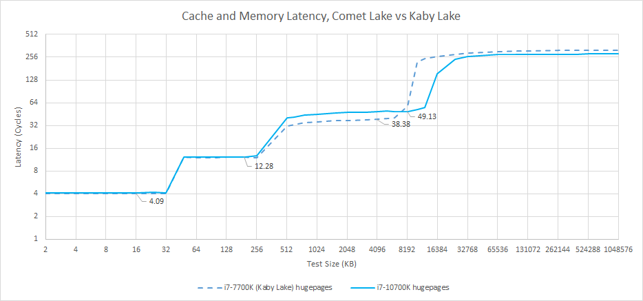
But after 2017, Intel’s cache setup no longer stood head and shoulders over everything else, because AMD made huge strides with their cache architecture. Zen 1 increased L1D size to match Skylake’s, at 32 KB. The L2 cache provided twice as much capacity as Skylake’s while maintaining 12 cycle latency. AMD’s engineers also gave themselves an easier problem to solve by sharing L3 across only four cores or less. As a result, Zen 1’s L3 can be accessed in roughly the same number of cycles as Kaby Lake’s.

Zen 2 continued this trend by doubling L3 size. At the same time, AMD took advantage of TSMC’s 7 nm process to increase clock speeds, lowering actual latency at all cache levels. The 3950X’s L3 latency ends up just above 8 ns, making it faster than Comet Lake’s L3 while also giving a single thread access to 16 MB of last level cache.
AMD’s massive improvements in cache bandwidth also eroded Skylake’s advantage. Zen 1’s L2 provides twice as much bandwidth per cycle as Piledriver’s, while the overhauled L3 design does a good job of catching up to Intel’s.
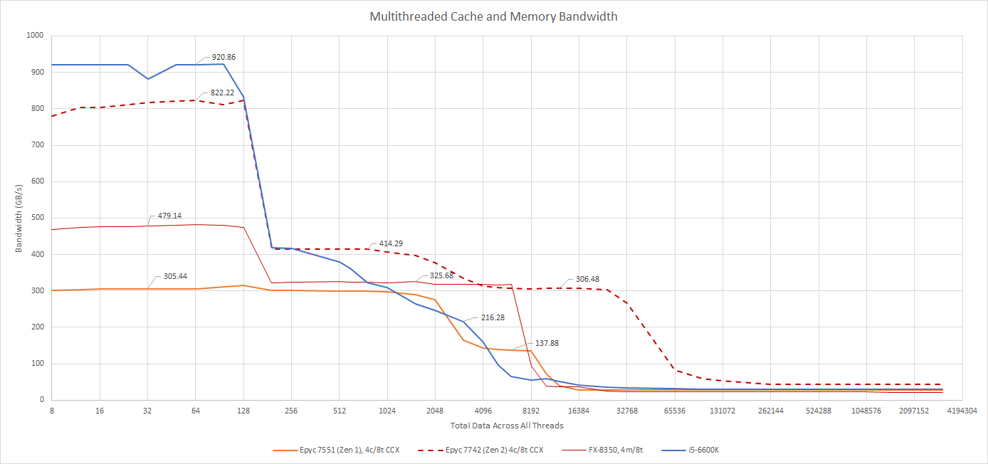
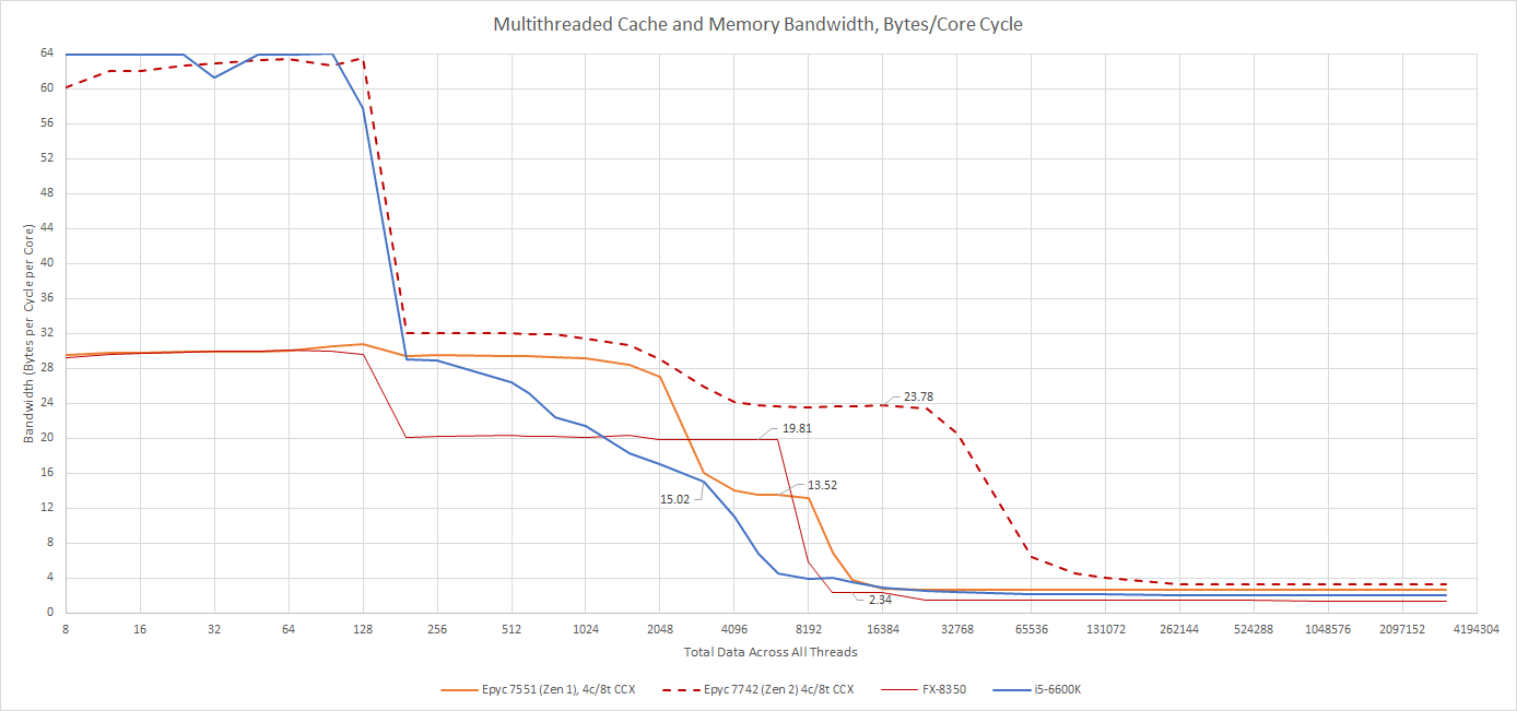
Within L1D sized regions, Skylake still maintains a large advantage over Zen 1, but Zen 2’s full width AVX execution changes that. When we get to L3, AMD’s Zen 2 shows off a very impressive L3 design that beats Skylake’s in all respects.
Skylake saw AMD catch up in other areas as well. Skylake’s 256-bit registers and execution units could give it a nice advantage in certain applications. Zen 1 split 256-bit instructions into two internal 128-bit operations, which would consume more execution engine resources. But Zen 2 introduced 256-bit registers and execution units, and Skylake’s vector performance advantage evaporated. AMD also increased core structure sizes with each generation, eroding Intel’s advantage.

To feed their beefier backend, AMD gave Zen a renamer that puts Skylake’s to shame. Zen can eliminate register to register MOVs even when they’re in a long dependency chain, while Skylake’s move elimination often fails in such a scenario. AMD also boosted renamer throughput to 5 instructions per cycle, or 6 micro-ops. That effectively makes Zen a 5-wide core, while Skylake remains 4-wide.
AMD’s instruction side bandwidth also saw massive improvements. At launch, Skylake enjoyed far superior instruction fetch bandwidth from its L2 and L3 caches, while Piledriver performed badly once it missed its L1i. After Zen, Skylake no longer enjoyed an instruction bandwidth advantage for large code footprints. When dealing with larger instructions (i.e., large immediates or AVX instructions), Skylake’s micro-op cache gave it a nice edge over Piledriver. But Zen erased that advantage too, with a micro-op cache of its own, and a larger one than Skylake’s to boot:

Zen 2 takes this further by increasing micro-op cache size to 4096 ops, making Skylake’s 1536 entry one look tiny by comparison. Zen 1 and 2 also made large improvements in their branch predictors, catching up to and then surpassing Skylake’s in accuracy.
But AMD didn’t surpass Skylake in all areas. Intel’s dated architecture still delivered very competitive vector performance. Skylake was also faster than Zen 1 or 2 when handling taken branches. AMD had been improving in that regard, and Zen finally introduced the ability to handle branches back to back. But Skylake was still faster at following branch targets when there were a lot of branches in play, and that advantage can’t be overstated. Both Zen 1 and Zen 2 can lose a lot of frontend bandwidth from wasted cycles after taken branches, meaning that Skylake can still pull ahead in very branchy but otherwise high IPC code.

On one hand, Intel’s repeated failures to replace Skylake meant that the company was stagnating, and forced to push an old architecture to its limits. But on the other hand, the way Skylake remained competitive so far into its service life shows that it’s an impressively solid architecture. Because Skylake wasn’t a huge leap over its predecessor, this also shows how strong of a foundation Intel built with Sandy Bridge and Haswell. AMD had to work for nearly half a decade and make use of a process node advantage before their per-core performance was competitive against Skylake.
Final Words
Client Skylake only slightly improves over Haswell, and doesn’t get a big situational performance boost from ISA extensions. Prior Intel architectures were more impressive. Sandy Bridge introduced 256-bit AVX support while delivering a large performance boost over Nehalem. Haswell added FMA and 256-bit vector integer support with the AVX2 instruction set extension, while delivering a decent performance increase over Sandy Bridge. I think Intel originally intended for Skylake to act as a stopgap until Cannon Lake and Sunny Cove could make their presence felt. But that’s not because Intel was being complacent.
Instead, Intel decided to shift their priorities for a generation. Client performance was de-prioritized in favor of spending more engineering effort on enabling different core configurations for client and server. This strategy made a lot of sense because Intel faced no serious competition after Haswell. AMD’s Piledriver was not competitive against Sandy Bridge, let alone later Intel’s later generations. Piledriver’s descendants, Steamroller and Excavator, didn’t see full desktop releases at all and weren’t scaled beyond 2 module, 4 thread configurations. AMD was so far behind that Intel’s only competition was older generations of their own products, and Skylake was going to succeed in the client market as long as it delivered some sort of improvement over Haswell.
Skylake did exactly that. It launched in 2015, faced no competition, and succeeded in the client market. Intel probably planned to release Cannon Lake across its client lineup a year or two after Skylake. If everything went well, Cannon Lake would benefit from Intel’s then new 10 nm process to deliver both performance and power consumption improvements. At the same time, it would bring AVX-512 support into client platforms, justifying some of the AVX-512 related design decisions made with Skylake (like the mask register file). Sunny Cove would show up not long after, and use much larger core structures along with many overdue improvements to put client performance back on track.
But as we all know, that strategy didn’t pan out. Cannon Lake never made it to desktop, or even high performance laptops. Sunny Cove was a disappointment too. It didn’t get a desktop launch until Intel backported it to 14 nm with Rocket Lake, and we all know how that went. Sunny Cove didn’t even get a high core count mobile SKU until 2021, when octa-core Tiger Lake was released. Skylake wound up holding the line year after year, while AMD raced to catch up with successive Zen generations. Zen 1 brought AMD’s per-core performance up to an acceptable level while using a core count advantage to challenge Intel’s multithreaded performance. With Zen 2, AMD’s per core performance became very competitive against Skylake, and only left Intel with a small lead in gaming. Finally, Zen 3 beat Skylake in nearly all respects, including taken branch handling.
For Intel, Skylake’s long life was definitely unplanned and not great for the company. But I wonder if the Skylake situation was a long term blessing for the PC scene. Intel had a monopoly over the high performance CPU market by the end of 2015. Their architecture was so advanced that, no one else could come close. Intel being stuck with Skylake for over half a decade gave AMD a chance to get back on their feet, bringing competition back to the CPU market.
To close, I think Skylake’s impact will be felt for quite a long time. Skylake variants are probably going to serve PC users well into the late 2020s. PC upgrade cycles tend to be quite long, and Skylake’s last refresh (Comet Lake) was only definitely superseded a year ago. Alder Lake and Zen 3 have definitely surpassed Skylake, but the Skylake architecture alone is still very strong and more than capable of handling every day tasks. Later Skylake variants, especially those with higher core counts and clock speeds in the upper 4 GHz range, still offer excellent performance. Beyond the architecture itself, Skylake’s long life is also responsible for the more competitive CPU scene we see today. AMD is back again after more than a decade of struggling behind Intel, and more competition means better prices and better products.
If you like our articles and journalism and you want to support us in our endeavors then consider heading over to our Patreon or our PayPal if you want to toss a few bucks our way or if you would like to talk with the Chips and Cheese staff and the people behind the scenes then consider joining our Discord.