
Examining Centaur CHA’s Die and Implementation Goals

In our last article, we examined Centaur’s CNS architecture. Centaur had a long history as a third x86 CPU designer, and CNS was the last CPU architecture Centaur had in the works before they were bought by Intel. In this article, we’ll take a look at Centaur CHA’s physical implementation. CHA is Centaur’s name for their system-on-chip (SoC) that targets edge server inference workloads by integrating a variety of blocks. These include:
Eight x86-compatible CNS cores running at up to 2.5 GHz
NCore, a machine learning accelerator, also running at 2.5 GHz
16 MB of L3 cache
Quad channel DDR4 controller
44 PCIe lanes, and IO links for dual socket support
We’re going to examine how CHA allocates die area to various functions. From there, we’ll discuss how Centaur’s design goals influenced their x86 core implementation.
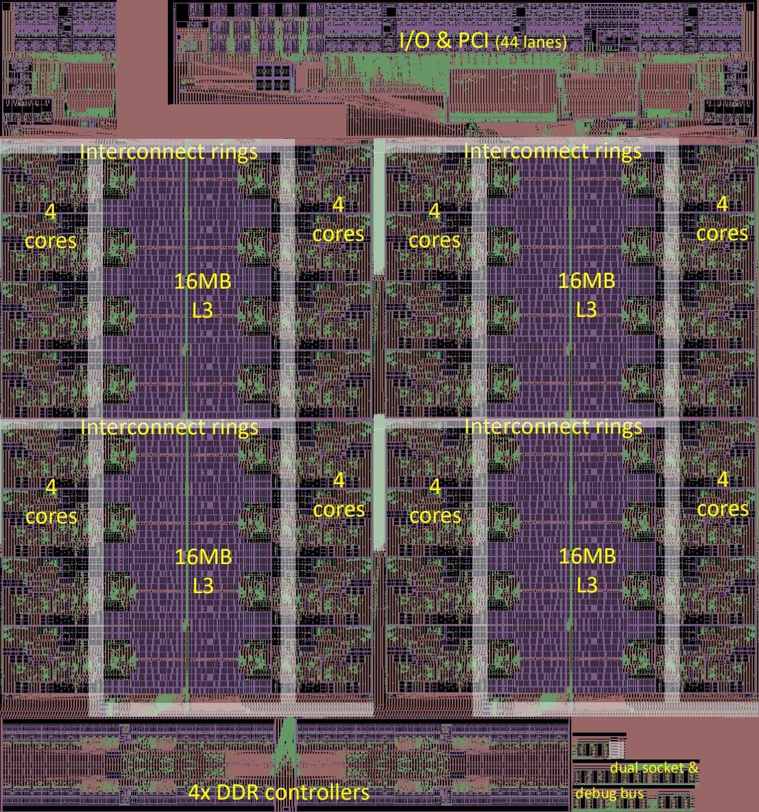
Compared to Haswell-E
Centaur says CNS has similar IPC to Haswell, so we’ll start with that obvious comparison. CHA is fabricated on TSMC’s 16nm FinFET process node, with a 194 mm2 die size. Haswell-E was fabricated on Intel’s 22nm FinFET process node and the 8 core die is 355 mm2. So by server and high end desktop standards, the CHA die is incredibly compact.
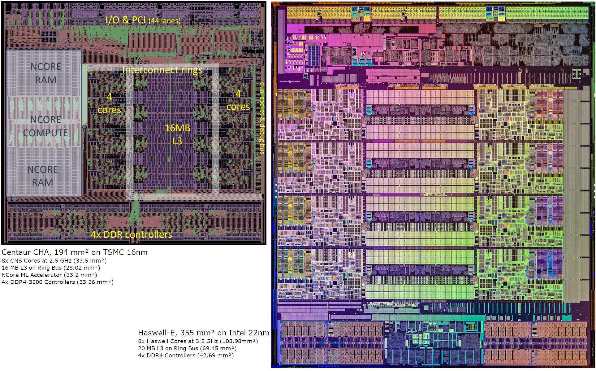
CHA ends up being just slightly larger than half of Haswell-E, even though both chips are broadly comparable in terms of core count and IO capabilities. Both chips have eight cores fed by a quad channel DDR4 controller, and support dual socket configurations. Differences from the CPU and IO side are minor. CHA has slightly more PCIe lanes, with 44 compared to Haswell-E’s 40. And Haswell has 20 MB of L3 cache, compared to 16 MB on CHA.
Now, let’s break down die area distribution a bit. The Haswell cores themselves occupy just under a third of the die. Add the L3 slices and ring stops, and we’ve accounted for about 50% of die area. The rest of the chip is used to implement IO.

CHA also has eight cores and similar amounts of IO. Like with Haswell-E, IO takes up about half the die. But the eight CNS cores and their L3 cache occupy a third of the die, compared to half on Haswell-E. That leaves enough die area to fit Centaur’s NCore. This machine learning accelerator takes about as much area as the eight CNS cores, so it was definitely a high priority for CHA’s design.

Centaur and Intel clearly have different goals. Haswell-E serves as a high end desktop chip, where it runs well above 3 GHz to achieve higher CPU performance. That higher performance especially applies in applications that don’t have lots of parallelism. To make that happen, Intel dedicates a much larger percentage of Haswell-E’s die area towards CPU performance. Haswell cores use that area to implement large, high clocking circuits. They’re therefore much larger, even after a process node shrink to Intel’s 14nm process (in the form of Broadwell).

In contrast, Centaur aims to make their cores as small as possible. That maximizes compute density on a small die, and makes room for NCore. Unlike Intel, CNS doesn’t try to cover a wide range of bases. Centaur is only targeting edge servers. In those environments, high core counts and limited power budget usually force CPUs to run at conservative clock speeds anyway. It’s no surprise that clock speed takes a back to seat to high density.
The result is that CNS achieves roughly Haswell-like IPC in a much smaller core, albeit one that can’t scale to higher performance targets. We couldn’t get a Haswell based i7-4770 to perfectly hit 2.2 GHz, but you get the idea:

7-Zip has a lot of branches, and a lot of them seem to give branch predictors a hard time. In our previous article, we noted that Haswell’s branch predictor could track longer history lengths, and was faster with a lot of branches in play. That’s likely responsible for Haswell’s advantage in 7-Zip. Unfortunately, we don’t have documented performance counters for CNS, and can’t validate that hypothesis.
Video encoding is a bit different. Branch performance takes a back seat to vector throughput. Our test uses libx264, which can use AVX-512. AVX-512 instructions account for about 14.67% of executed instructions, provided the CPU supports them. CNS roughly matches Haswell’s performance per clock in this scenario. But again, Haswell is miles ahead when the metaphorical handbrake is off:

CNS is most competitive when specialized AVX-512 instructions come into play. Y-Cruncher is an example of this, with 23.29% of executed instructions belonging to the AVX-512 ISA extension. VPMADD52LUQ (12.76%) and VPADDQ (9.06%) are the most common AVX-512 instructions. The former has no direct AVX2 equivalent as far as I know.
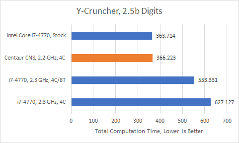
Even though its vector units are not significantly more powerful than Haswell’s, CNS knocks this test out of the park. At similar clock speeds, Haswell gets left in the dust. It still manages to tie CNS at stock, showing the difference high clock speeds can make. We also can’t ignore Haswell’s SMT capability, which helps make up some of its density disadvantage.
Compared to Zeppelin and Coffee Lake
Perhaps comparisons with client dies make more sense, since they’re closer in area to CHA. AMD’s Zeppelin (Zen 1) and Intel’s Coffee Lake also contain eight cores with 16 MB of L3. Both are especially interesting because they’re implemented on process nodes that are vaguely similar to CHA’s.
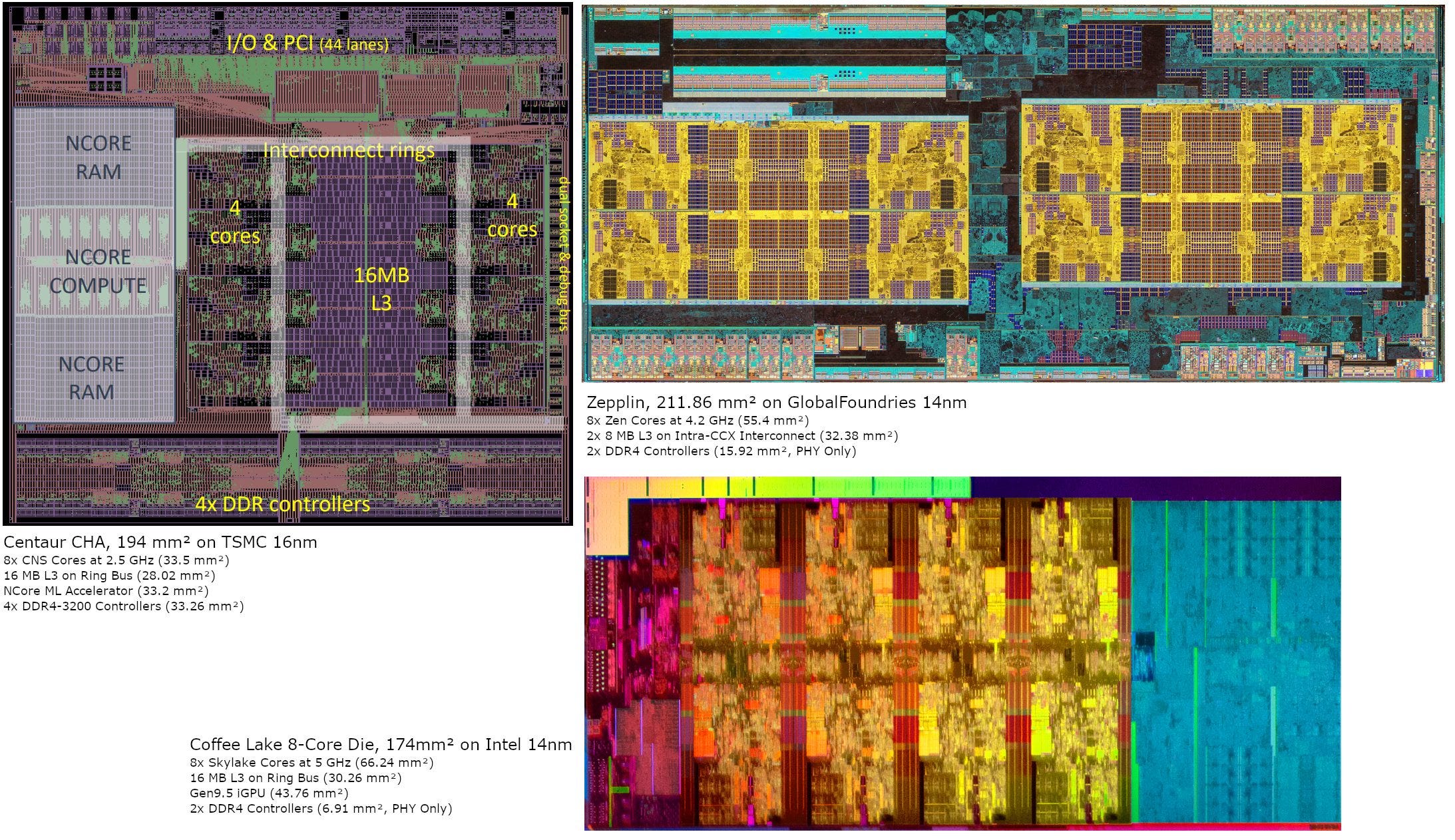
Let’s start with Zeppelin. This AMD die implements eight Zen 1 cores in two clusters of four, each with 8 MB of L3. It’s about 9% larger than CHA, but has half as many DDR4 channels. Zeppelin has fewer PCIe lanes as well, with 32 against CHA’s 44.

L3 area is in the same ballpark on both Zeppelin and CHA, suggesting that TSMC 16nm and GlobalFoundries 14nm aren’t too far apart when high density SRAM is in play. Core area allocation falls between CHA and Haswell-E’s, although percentage-wise, it’s closer to the latter.
A lot of space on Zeppelin that doesn’t belong to cores, cache, DDR4, or PCIe. That’s because Zeppelin is a building block for everything. Desktops are served with a single Zepplin die that provides up to eight cores. Workstations and servers get multiple dies linked together to give more cores, more memory controller channels, and more PCIe. In the largest configuration, a single Epyc server chip uses four Zeppelins to give 32 cores, eight DDR4 channels, and 128 PCIe lanes.
Zeppelin’s flexibility lets AMD streamline production. But nothing in life is free, and die space is used to make that happen. For client applications, Zeppelin tries to bring a lot of traditional chipset functionality onto its die. It packs a quad port USB 3.1 controller. That takes space. Some PCIe lanes can operate in SATA mode to support multi-mode M.2 slots, which means extra SATA controller logic. Multi-die setups are enabled by cross-die links (called Infinity Fabric On Package, or IFOP), which cost area as well.
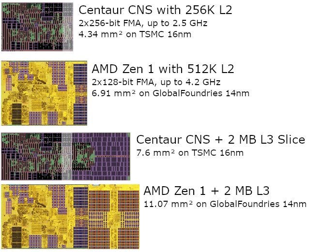
AMD’s Zen 1 core was probably designed with that in mind. It can’t clock low because it has to reach desktop performance levels, so density is achieved by sacrificing vector performance. Zen 1 uses 128-bit execution units and registers, with 256-bit AVX instructions split into two micro-ops.
Then, Zen 1 took aim at modest IPC goals, and gave up on extremely high clock speeds. That helps improve their compute density, and lets them fit eight cores in a die that has all kinds of other connectivity packed into it. Like Haswell, Zen uses SMT to boost multithreaded performance with very little die area overhead.

In its server configuration, Zen 1 can’t boost as high as it can on desktops. But it still has a significant clock speed advantage over CNS on low threaded parts of workloads. Like Haswell, Zen 1 delivers better performance per clock than CNS with 7-Zip compression.

With video encoding, CNS again falls behind. Part of that is down to clock speed. Zen 1’s architecture is also superior in some ways. AMD has a large non-scheduling queue for vector operations, which can prevent renamer stalls when lots of vector operations are in play. In this case, that extra “fake” scheduling capacity seems to be more valuable than CNS’s higher execution throughput.

Finally, CNS leaves Zen 1 in the dust if an application very heavy on vector compute, and can take advantage of AVX-512. In Y-Cruncher, Zen 1 is no match for CNS.
Intel’s Coffee Lake
Coffee Lake’s die area distribution looks very different. Raw CPU performance is front and center, with CPU cores and L3 cache taking more than half the die.

About a quarter of Coffee Lake’s die goes to an integrated GPU. In both absolute area and percentage terms, Comet Lake’s iGPU takes up more space than Centaur’s NCore, showing the importance Intel places on integrated graphics. After the cores, cache, and iGPU are accounted for, there’s not much die area left. Most of it is used to implement modest IO capabilities. That makes Coffee Lake very area efficient. It packs more CPU power into a smaller die than CHA or Zeppelin, thanks to its narrow focus on client applications.
Like Haswell and Zen, the Skylake core used in Coffee Lake looks designed to reach very high clocks, at the expense of density. It’s much larger than CNS and Zen 1, and clocks a lot higher too.

Intel also sacrifices some area to make Skylake “AVX-512 ready”, for lack of a better term. This lets the same basic core design go into everything from low power ultrabooks to servers and supercomputers, saving design effort.
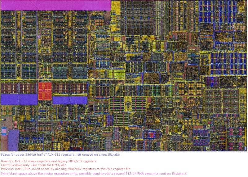
Perhaps it’s good to talk about AVX-512 for a bit, since that’s a clear goal in both Skylake and CNS’s designs.
AVX-512 Implementation Choices
CNS’s AVX-512 implementation looks focused on minimizing area overhead, rather than maximizing performance gain when AVX-512 instructions are used. Intel has done the opposite with Skylake-X.
To summarize some AVX-512 design choices:

To me, CNS is very interesting because it shows how decent AVX-512 support can be implemented with as little cost as possible. Furthermore, CNS demonstrates that reasonably powerful vector units can be implemented in a core that takes up relatively little area. To be clear, this kind of strategy may not offer the best gains from AVX-512:

But it can still offer quite a bit of performance improvement in certain situations, as the benchmark above shows.
Thoughts about Centaur’s Design
Centaur aimed to create a low cost SoC that combines powerful inference capabilities with CPU performance appropriate for a server. Low cost means keeping die area down. But Centaur’s ML goals mean dedicating significant die area toward its NCore accelerator. Servers need plenty of PCIe lanes for high bandwidth network adapters, and that takes area too. All of that dictates a density oriented CPU design, in order to deliver the required core count within remaining space.
To achieve this goal, Centaur started by targeting low clocks. High clocking designs usually take more area, and that’s especially apparent on Intel’s designs. There are tons of reasons for this. To start, process libraries designed for high speeds occupy more area than ones designed for high density. For example, Samsung’s high performance SRAM bitcells occupy 0.032 µm² on their 7nm node, while their high density SRAM takes 0.026 µm². Then, higher clock speeds often require longer pipelines, and buffers between pipeline stages take space. On top of that, engineers might use more circuitry to reduce the number of dependent transitions that have to complete within a cycle. One example is using carry lookahead adders instead of simpler carry propagate adders, where additional gates are used to compute whether a carry will be needed at certain positions, rather than wait for a carry signal to propagate across all of a number’s binary digits.
Then, AVX-512 is supported with minimal area overhead. Centaur extended the renamer’s register alias table to handle AVX-512 mask registers. They tweaked the decoders to recognize the extra instructions. And they added some execution units for specialized instructions that they cared for. I doubt any of those took much die area. CNS definitely doesn’t follow Intel’s approach of trying to get the most out of AVX-512, which involves throwing core area at wider execution units and registers.
Finally, Centaur set modest IPC goals. They aimed for Haswell-like performance per clock, at a time when Skylake was Intel’s top of the line core. That avoids bloating out-of-order execution buffers and queues to chase diminishing IPC gains. To illustrate this, let’s look at simulated reorder buffer (ROB) utilization in an instruction trace of a 7-Zip compression workload. A CPU’s ROB tracks all instructions until their results are made final, so its capacity represents an upper bound for a CPU’s out of order execution window. We modified ChampSim to track ROB occupancies every cycle, to get an idea of how often a certain number of ROB entries are utilized.

Most cycles fall into one of two categories. We either see less than 200 entries used. Or the ROB is basically filling up, indicating it’s not big enough to absorb latency. We can also graph the percentage of cycles for which ROB utilization is below a certain point (below). Again, we see clearly diminishing returns from increased reordering capacity.

Increasing ROB size implies beefing up other out-of-order buffers too. The renamed register files, scheduler, and load/store queues will have to get bigger, or they’ll fill up before the ROB does. That means IPC increases require disproportionate area tradeoffs, and Centaur’s approach has understandably been conservative.
The resulting CNS architecture ends up being very dense and well suited to CHA’s target environment, at the expense of flexibility. Under a heavy AVX load, the chip draws about 65 W at 2.2 GHz, but power draw at 2.5 GHz goes up to 140 W. Such a sharp increase in power consumption is a sign that the architecture won’t clock much further. That makes CNS completely unsuitable for consumer applications, where single threaded performance is of paramount importance. At a higher level, CHA also ends up being narrowly targeted. Even though CNS cores are small, each CHA socket only has eight of them. That’s because Centaur spends area on NCore and uses a very small die. CHA therefore falls behind in multi-threaded CPU throughput, and won’t be competitive in applications that don’t use NCore’s ML acceleration capabilities.
Perhaps the biggest takeaway from CNS is that it’s possible to implement powerful vector units a physically small core, as long as clock speed and IPC targets are set with density in mind.

Centaur did all this with a team of around 100 people, on a last-generation process node. That means a density oriented design is quite achievable with limited resources. I wonder what AMD or Intel could do with their larger engineering teams and access to cutting edge process nodes, if they prioritized density.
What Could Have Been?
Instead of drawing a conclusion, let’s try something a little different. I’m going to speculate and daydream about how else CNS could have been employed.
Pre-2020 – More Cores?
CHA tries to be a server chip with the die area of a client CPU. Then it tries to stuff a machine learning accelerator on the same die. That’s crazy. CHA wound up with fewer cores than Intel or AMD server CPUs, even though CNS cores prioritized density. What if Centaur didn’t try to create a server processor with the area of a client die?
If we quadruple CHA’s 8-core CPU complex along with its cache, that would require about 246 mm2 of die area. Of course, IO and connectivity would require space as well. But it’s quite possible for a 32 core CNS chip to be implemented using a much smaller die than say, a 28-core Skylake-X chip.
A fully enabled 28 core Skylake-X chip would likely outperform a hypothetical 32 core CNS one. But Intel uses 677.98 mm2 to do that. A few years ago, Intel also suffered from a shortage of production capacity on their 14nm process. All of that pushes up prices for Skylake-X. That gives Centaur an opportunity to undercut Intel. Using a much smaller die on a previous generation TSMC node should make for a cheap chip.
Before 2019, AMD could also offer 32 cores per socket with their top end Zen 1 Epyc SKUs. Against that, CNS would compete by offering AVX-512 support and better vector performance.
Post 2020 – A Die Shrink?
But AMD’s 2019 Zen 2 launch changes things. CNS’s ability to execute AVX-512 instructions definitely gives it an advantage. But Zen 2 has 256-bit execution units and registers just like CNS. More importantly, Zen 2 has a process node advantage. AMD uses that to implement a more capable out-of-order execution engine, more cache, and faster caches. That puts CNS in a rough position.

Core for core, CNS stands no chance. Even if we had CNS running at 2.5 GHz, its performance simply isn’t comparable to Zen 2. It gets worse in file compression:

Even in Y-Cruncher, which is a best case for CNS, Zen 2’s higher clocks and SMT support let it pull ahead.

Worse, TSMC’s 7nm process lets AMD pack 64 of those cores into one socket. In my view, CNS has to be ported to a 7nm class process to have any chance after 2020. It’s hard to guess what that would look like, but I suspect a CNS successor on 7nm would fill a nice niche. It’d be the smallest CPU core with AVX-512 support. Maybe it could be an Ampere Altra competitor with better vector performance.
Under Intel, CNS could bring AVX-512 support to E-Cores in Intel’s hybrid designs. That would fix Alder Lake’s mismatched ISA awkwardness. Compared to Gracemont, CNS probably wouldn’t perform as well in integer applications, but vector performance would be much better. And CNS’s small core area would be consistent with Gracemont’s area efficiency goal. Perhaps a future E-Core could combine Gracemont’s integer prowess with CNS’s vector units and AVX-512 implementation.
If you like our articles and journalism and you want to support us in our endeavors then consider heading over to our Patreon or our PayPal if you want to toss a few bucks our way or if you would like to talk with the Chips and Cheese staff and the people behind the scenes then consider joining our Discord.