
Intel’s Tremont: Atom Changes Course

Today we’ll look at Intel’s Tremont architecture to put Gracemont in perspective. It’s Gracemont’s direct ancestor, and represents a shift in Intel’s Atom strategy. It delivers a massive 30% performance-per-clock jump – at least according to Intel – over its predecessor, Goldmont Plus. At the same time, Tremont debuted several techniques that feature prominently in Gracemont.
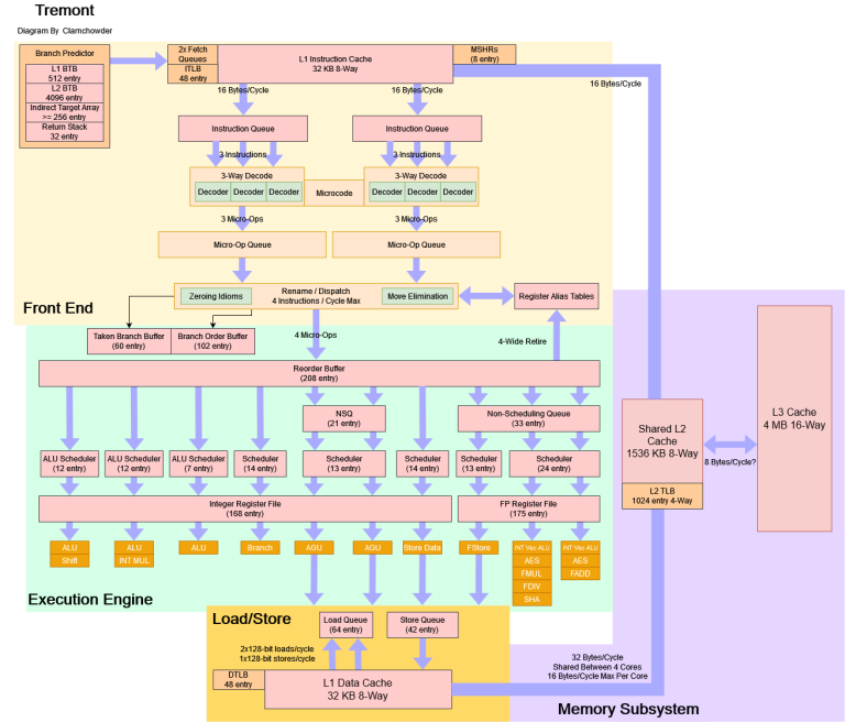
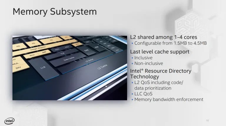
Block Diagram
Tremont looks like a smaller Gracemont or alternatively, Gracemont looks like a bigger Tremont:
Branch Prediction
As we mentioned in the previous article, accurate branch prediction is great for both performance and power efficiency so we’ll have Intel themselves introduce Tremont’s branch predictor:
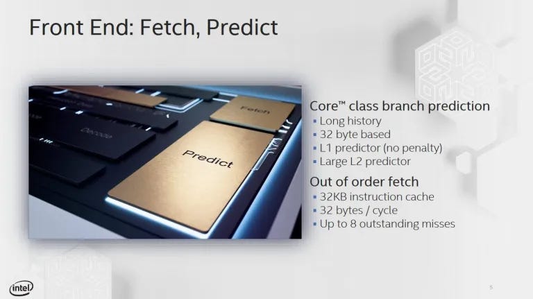
Compared to previous architectures, Tremont’s out of order decode scheme means branch prediction is even more important. Because its fetch and decode clusters reach farther ahead than a traditional decoder does, an incorrect prediction could have a heavy impact on fetch and decode bandwidth. Thankfully, Intel wasn’t kidding around when they went for “Core class branch prediction”.
Pattern Recognition
We can confirm Tremont’s predictor is indeed quite capable, with long history length tracking:
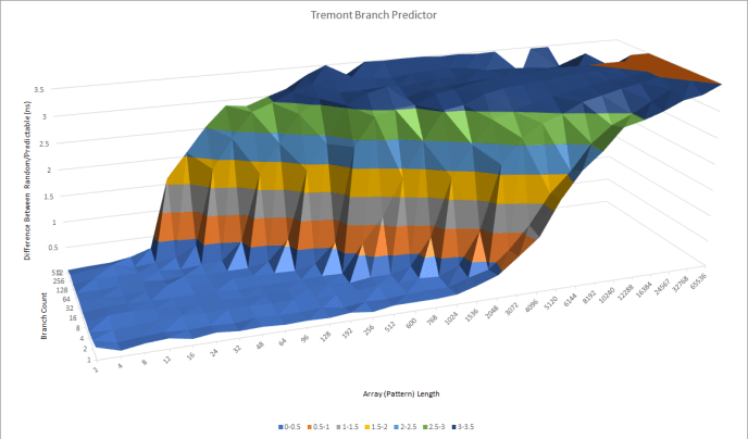
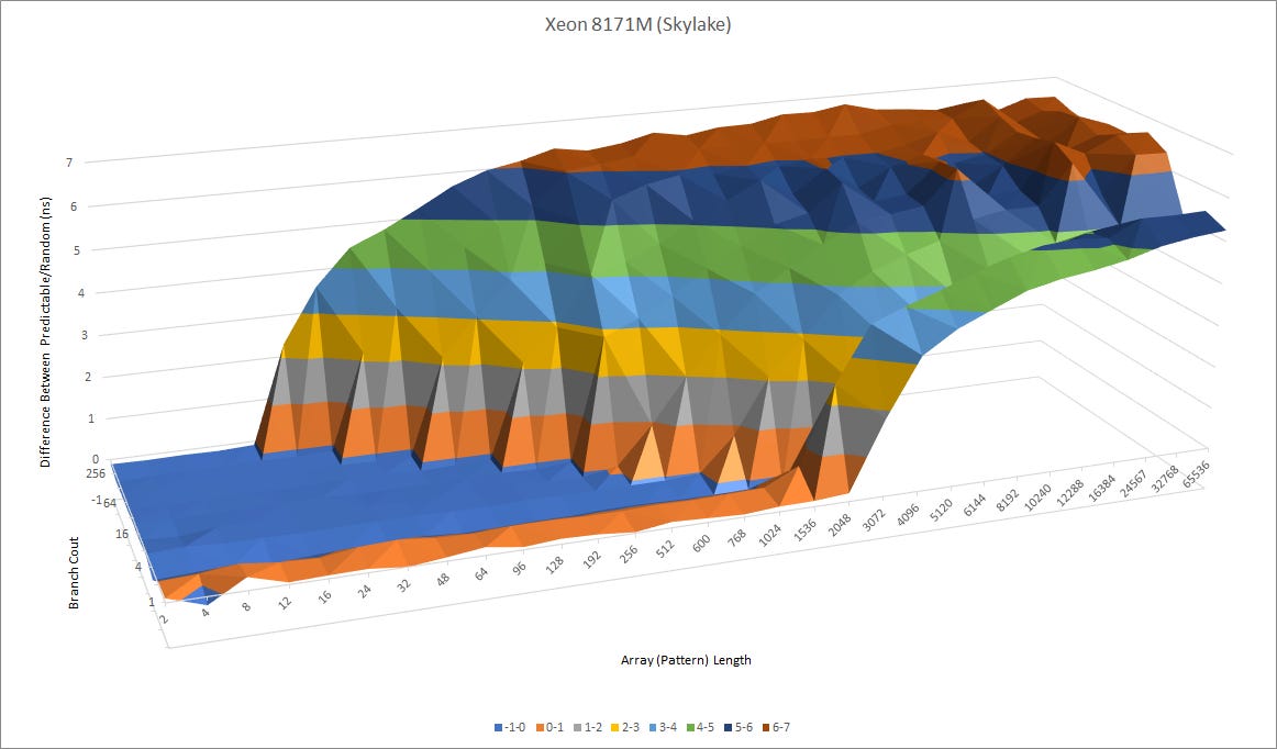
When Tremont was presented in 2019, Intel’s top of the line desktop CPUs still relied on the Skylake architecture and Tremont is definitely in the same class. We can also see a gentle increase in prediction latency at longer history lengths, confirming that Intel’s using an overriding L2 predictor. Unlike Zen 1 and Zen 2 though, Intel’s L1 predictor is already very capable. Even at history lengths approaching the branch predictor’s capabilities, there’s little increase in time per branch which suggests the L2 predictor rarely needs to override the first level.

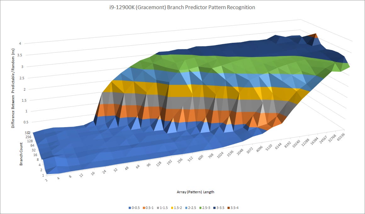
However compared to Gracemont, Tremont definely looks a generation behind. Clearly, Intel was determined to push hard on performance with Gracemont and needed branch prediction capabilities to match.
Branch Target Tracking
After determining whether the branch is taken, the predictor must tell the fetch unit where it thinks the branch will go. For that, Tremont uses a 4096 entry branch target buffer (BTB), split into two levels:
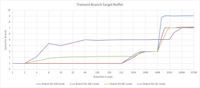
Tremont can do back to back predictions for up to 512 branch targets and the L2 BTB can track up to 4096 branch targets, though hitting that second level will cost two extra cycles in the frontend. Here’s a condensed comparison against BTBs in Intel’s “Core” lineup:

Compared to “Core” class predictors, Tremont’s target tracking capacity is similar, though Intel puts another pipeline stage in front of the L2 BTB to keep power consumption under control. However, Tremont’s ability to do zero bubble predictions is quite impressive compared to other Intel architectures, and is only bested by Gracemont and AMD’s Zen 3.
Real World Branch Predictor Performance
In terms of accuracy, Tremont’s direction predictor turns in a competent performance and it’s a bit like Gracemont compared to Golden Cove.
Performance Impact
Tremont has very advanced performance monitoring capabilities, which might hint at high performance aspirations. “Topdown” counters can break down bottlenecks at pipeline slot granularity. Similar counters are carried over to Gracemont, letting us see how Intel has progressed:
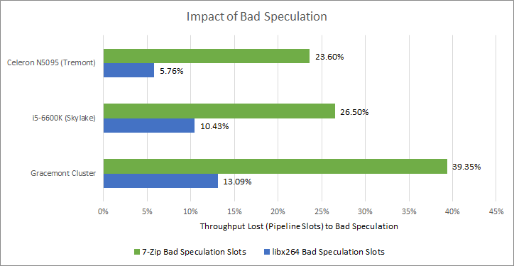
Even with an inferior branch predictor, Tremont loses fewer slots to branch mispredicts. This is partly because Gracemont’s larger reordering window lets it speculate farther ahead, meaning it has more to lose from a mispredict. Looking at the mispredicted area in our pattern recognition tests suggest Gracemont takes an additional cycle to detect a mispredict (pipeline length). If Intel wants Gracemont’s successor to hit even higher performance targets while maintaining excellent power efficiency, they’ll have to focus very hard on the branch predictor.
Frontend – Bringing Those Instructions In
Clustered Fetch and Decode
When we get to instruction fetch and decode, Tremont’s frontend gets one of the most eye catching changes: an out-of-order decoder arranged as two three-wide clusters. At first glance, this sounds impressive because every other CPU I’m aware of has used a strictly in-order frontend, with out-of-order execution only applying to the backend. However on deeper analysis, this design isn’t geared toward outright performance instead, it aims to increase frontend throughput with minimal area, power, and engineering time cost.
The low level characteristics of the microarchitecture within each decode cluster remain the same as in the Goldmont Plus microarchitecture. For example, instructions should avoid more than 4 Bytes of prefixes and escapes
Intel 64 and IA-32 Architectures Optimization Reference Manual, Section 4.1.2
The two clusters are likely two Goldmont Plus decoders, copy/pasted. Intel would save R&D effort by leaning on a validated and deployed block of logic with well known characteristics. For example, there’s no need to modify the instruction queue to let more decoders de-queue blocks of bytes from it, or tweak the micro-op queue to accept more micro-ops per cycle and, the on demand length decode circuit can remain unchanged. So, Tremont’s frontend looks a bit like this:
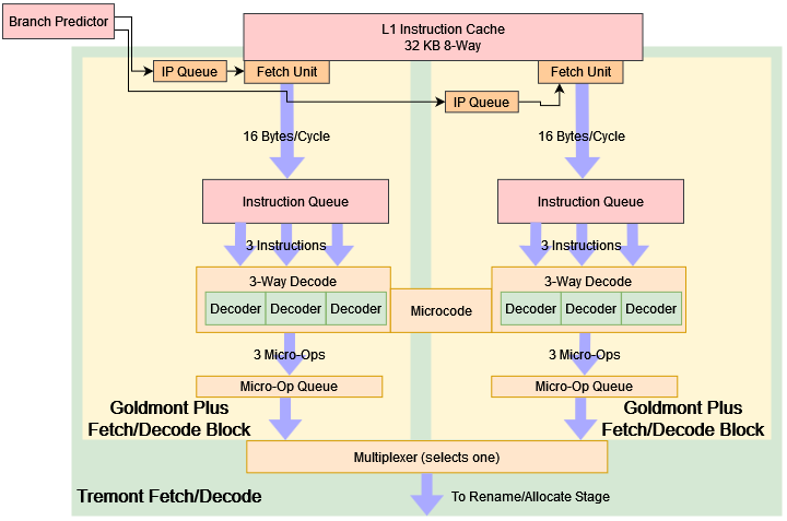
To make the two clusters work together, Intel uses the branch predictor as a simple and elegant form of glue. Taken branches are naturally present in real world code, at a rate of approximately one every ten to twenty instructions. The branch predictor already tracks where these branches go, in order to steer the fetch unit. Instead of feeding one fetch unit’s target queue, the Tremont’s predictor alternates between the two clusters, so that each cluster gets every other taken branch target and a multiplexer at the end stitches the instruction stream back together in exactly the same way.
But if taken branches are too far apart, the decoders will act like a single 3-wide decoder, rather than a 6-wide one. Intel is well aware of this, and their optimization manual notes “Inserting unconditional JMP instructions to the next sequential instruction pointer at intervals between 16 to 32 instructions may relieve this bottleneck if encountered.”
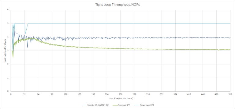
From our testing, Tremont’s decoder starts behaving like a 3-wide one after around 128 to 160 instructions without a taken branch. Its throughput peaks with 3 to 64 instructions in the loop. Average applications have 5% to 20% branches, and about half of those are taken so Tremont’s lack of automatic load balancing between the clusters shouldn’t be a big issue.
Instruction Side Bandwidth
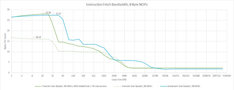
With a plain stream of NOPs, Tremont gets stuck on one decode cluster, and only achieves 16 bytes per cycle and it also has trouble getting full instruction bandwidth from L2. If we add unconditional jumps in to help Tremont load balance the clusters, L1 instruction cache bandwidth is similar to Gracemont’s at which point, Tremont’s biggest disadvantage is its smaller 32 KB instruction cache.
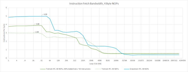
With 4 byte NOPs, we can test the decoders instead of L1i bandwidth. Again, our simple test from previous articles gets stuck on one cluster and only achieves 3 instructions per cycle. Adding taken branches removes the frontend bottleneck completely, and Tremont looks just like Gracemont. Both are limited by their rename stages.
From L2, Tremont and Gracemont can’t sustain 4 instructions per cycle the way big cores can. That’s probably due to a combination of higher L2 latency and less aggressive instruction-side prefetching. These little cores really want to hit the L1 instruction cache – more so that Sunny Cove and Golden Cove do. So, Intel increasing Gracemont’s L1i capacity to 64 KB makes a lot of sense. Alternatively, Intel could have reduced L2 latency and allowed deeper prefetching after a L1i miss but that means moving more data around, and data movement costs power.
Rename/Allocate
The rename and allocate stage serves as a bridge between the frontend and the out-of-order backend. With a 6-wide frontend, Tremont joins the club of x86 CPUs limited by rename width:

Tremont’s rename capabilities are slightly weaker than those of Skylake.
The renamer can recognize xor r,r, as independent but doesn’t eliminate them, meaning that they still require ALU ports. Independent MOVs can be eliminated, allowing a throughput of more than three per cycle. Dependent register to register MOVs can occasionally be eliminated, but the mechanism isn’t as bulletproof as the ones in Gracemont, Sunny Cove, or AMD’s Zen 2/3.

Still, Tremont’s renamer makes a reasonable tradeoff between reducing complexity and improving performance. Haswell and Skylake have similar move elimination capabilities, and Haswell’s performance counters show that move elimination succeeds more often than not. That suggests chained register to register MOVs are rare in practice. Similarly, compilers like GCC, Clang, and MSVC use xor r,r to zero registers (bitwise exclusive or with identical values will always result in zero). Taking care of those common cases already goes a long way. A more capable renamer might buy a little more performance, but with Tremont, Intel’s engineers probably decided it wasn’t worth the transistors.
Backend Resources
Tremont’s instruction reordering window is impressive for an Atom core. In many areas, it’s comparable to Haswell (HSW) and Skylake (SKL).

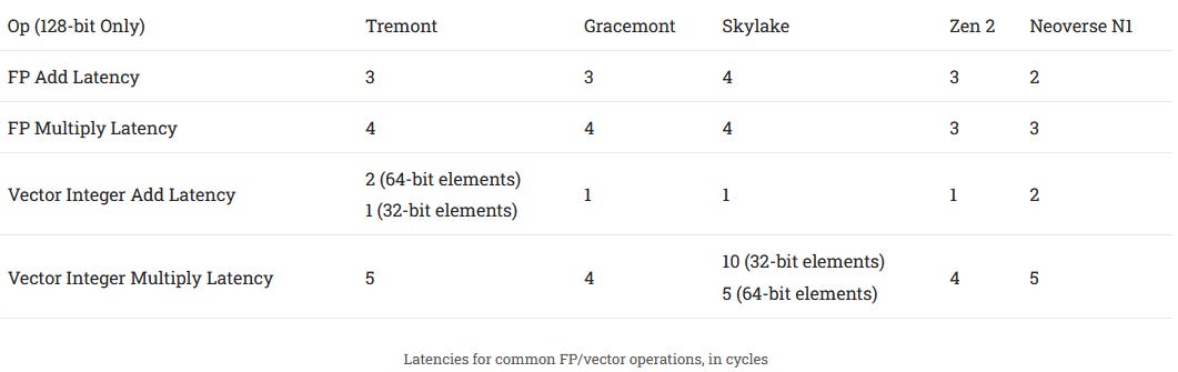
Unlike Haswell and Skylake, Tremont doesn’t focus on throughput and as such it completely lacks AVX support meaning its vector registers are 128-bit. That lets Intel increase the number of vector registers to a number comparable to that of HSW and SKL, while consuming less area and power. Because Tremont lacks SMT support, it doesn’t have to spend registers saving architectural register state for a second thread which means more of Tremont’s integer and FP registers can go towards renaming capacity.
Scheduling and Execution
Like other Atoms and AMD’s Zen 1/2, but unlike Intel’s Core CPUs, Tremont uses distributed integer scheduling queues. In total, we think Tremont has 45 scheduler entries on the integer side, but it’s not that simple. One execution port and its associated queue only handles branch instructions, leaving 31 entries available for common integer instructions. For comparison, Zen 2’s distributed scheduler has 64 entries, and is more flexible. All 64 entries are available for common integer operations, and half of those can be used for branches. Skylake is down a few entries compared to Zen 2, but still has way more than Tremont. And more importantly, Skylake’s unified scheduler can make each entry go further, because any entry can be used for any port.
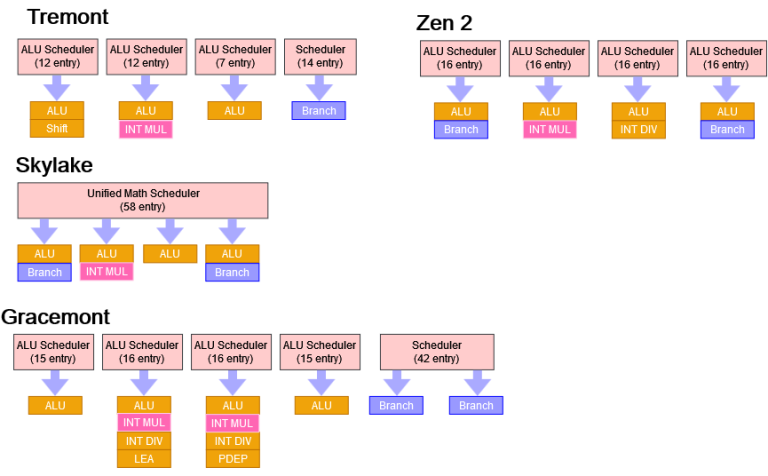
Next to Skylake and Zen 2, Tremont’s integer scheduler looks like it prioritizes low power at the expense of performance. Gracemont dramatically increases integer scheduling capacity and looks a lot more like a big core.
Tremont’s three ALU ports shouldn’t be a bottleneck in most cases, since the renamer can only feed the backend with four instructions per cycle. Even in pure integer workloads, those integer instructions will be mixed with branches (which go to a separate port on Tremont) and memory accesses but port count isn’t everything. Tremont has a slightly weak integer multiplier:

Tremont makes similar sacrifices with other less common integer operations. For example, LEA, bitwise rotate, and bit test/set instructions only go to one port. Big cores like Skylake and Zen have multiple ports for those operations.
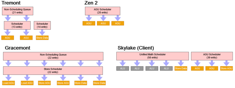
For memory scheduling, Tremont combines small scheduling queues with a moderately sized non-scheduling queue. That lets it reduce scheduler power while not stalling the renamer if more than 13 memory instructions are waiting to execute. This scheme might not be as effective at extracting instruction level parallelism as a plain 34 entry scheduler, since only the first 13 memory instructions can be checked for execute-readiness but it should be much more power efficient.
In terms of execution throughput, Tremont can do two 128-bit memory operations per cycle, one of which can be a store. That’s similar to Sandy Bridge. It’s nothing impressive, but shouldn’t be a bottleneck in most applications.
Tremont’s floating point side looks like a mini-Gracemont. The floating point scheduler by itself is small with only 24 entries but a 33 entry non-scheduling queue lets Tremont’s backend have 57 floating point instructions waiting to execute before stalling the renamer. That’s basically the same as Skylake’s floating point scheduling capacity.
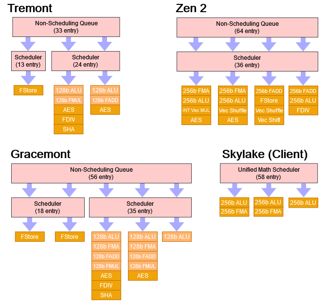
Again, Tremont can’t examine all 57 of those instructions every cycle to see if they’re ready to execute, so an instruction too far ahead may end up waiting in the non-scheduling queue even if an execution unit is available. But Skylake doesn’t have a clear advantage either because some of those unified scheduler entries will be used by integer instructions, since many FP/vector heavy workloads still have a lot of integer instructions.
Vector throughput is one of the weakest areas for Tremont. AVX support is completely missing so rendering, image manipulation, and video encoding will have to make do with 128-bit SSE instructions. No FMA (fused multiply add) further reduces floating point throughputso even with SSE, throughput is unexpectedly weak. For example, Tremont could only do one 2×64-bit integer addition per clock, even though Intel shows two ports to vector ALUs in their block diagram. 4×32-bit add executes at a rate of two per clock. Latency is worse with 64-bit elements too. Speaking of latencies:
Lack of AVX support is reasonable for an efficiency oriented core. But in a hybrid configuration, lack of AVX support prevents applications from taking advantage of the big core’s vector throughput. That’s because the operating system can move processes between cores at any time, should a program starts on a big core, detects AVX support, and later gets moved to a little core, it’ll crash if it tries to execute an AVX instruction. Intel corrected this deficiency in Gracemont.
But enough numbers and theoretical comparisons, let’s see what happens in practice:
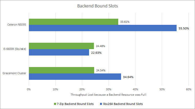
Tremont stalls a lot more on a full backend than Gracemont and Skylake. While this doesn’t seem good at first glance, remember that CPUs use a large reordering window to “hide” time taken by long latency instructions. These long latency instructions are often L1 data cache misses and as we’ll see later, Tremont in Jasper Lake form does not have an impressive memory hierarchy. Now, let’s break down those backend-caused stalls:
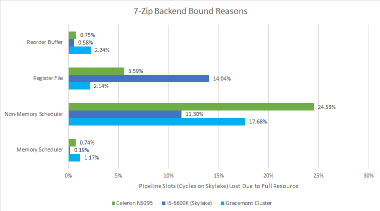
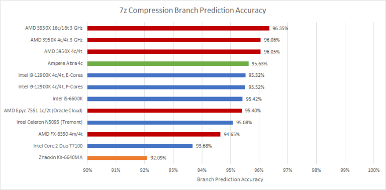
7-Zip compression is a pure integer workload, and Tremont’s integer scheduler struggles. Skylake’s larger unified scheduler does better, pushing the limiting factor to the integer registers. With a larger integer scheduler and register file, Gracemont is a welcome improvement. However, none of the three CPUs here make good use of their ROB capacity.
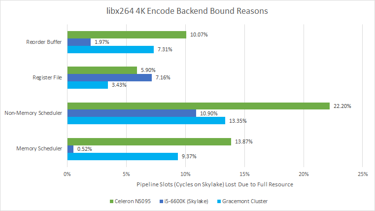
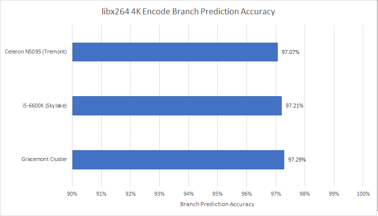
libx264 video encoding is a different story. It’s a well vectorized workload, and Tremont has a tough time. Again, Tremont’s distributed scheduler struggles to hide latency. The memory scheduler with its non-scheduling queue does better, but still causes a lot of stalls. The register files are also filling a bit, though it’s not bad enough to be embarrassing. Finally, some backend bound slots (10%) are attributed to the ROB filling. In a way, that’s good, because that means some other resource didn’t get exhausted first and ROB capacity is being well utilized. On the other, it means there’s too much latency for the core to handle without stalling.
Gracemont does better in all respects, thanks both to its bigger out-of-order resources and Alder Lake’s superior memory subsystem. Skylake does even better. Its unified math scheduler can bring its entire capacity into play regardless of whether the application is spamming integer or floating point instructions. Its smaller but wider vector register file suffers a bit compared to Gracemont – 85% of the register file related stalls were because the vector register file filled up. Skylake’s higher bandwidth and lower latency cache comes into play too, and are probably responsible for its lack of ROB stalls and overall performance win (coming in a hair ahead of Gracemont, even at a lower clock).
Cache and Memory Access
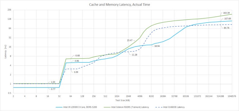
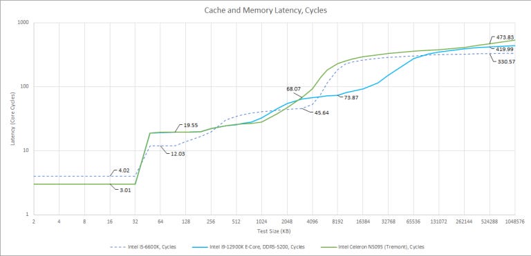
Tremont’s memory hierarchy is similar to Gracemont’s, which is to be expected, but weaker all around because Tremont focuses more on low power then Gracemont.
Latency
Gracemont and Tremont’s L1D and L2 caches have the same latency in clock cycles, but Gracemont clocks higher. Tremont’s L2 is smaller as well, at 1.5 MB compared to Gracemont’s 2 MB. When we get to L3, Tremont has lower latency in clock cycles, but higher actual latency because of its low clock speed. Gracemont has an advantage there, thanks to Alder Lake’s shared L3. It’s not fast either, but at 30 MB it’s a lot bigger.
Address Translation
Again, Tremont is very similar to Gracemont. Both have fully associative L1 DTLBs, which are a touch smaller than the ones found on big cores and, both have 4-way associative L2 TLBs with 9 cycles of extra latency. However, Tremont’s L2 TLB is smaller, meaning it’ll suffer more in applications with large memory footprints or scattered accesses. For a comparison with the big core line, it’s similar in capacity to Haswell’s.

From Tremont to Gracemont, the Atom line got the same L2 TLB coverage increase as the Core line did from Haswell to Sunny Cove. Gracemont (and Tremont) both make sacrifices though. Latency to the L2 TLB is higher, and associativity is lower. Higher latency means less work has to be done in each pipeline stage, while lower associativity means fewer tag comparisons are needed to check for a hit. So both of those differences are likely down to Atom’s focus on efficiency.
Bandwidth
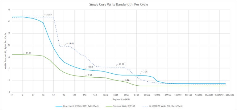
In bandwidth testing for our last article, we saw Gracemont getting its lunch money taken by big cores with full-width AVX support and Tremont does even worse.
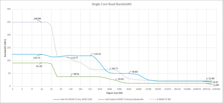
Starting with read bandwidth and a single thread, Tremont is hammered by low clock speed and narrow datapaths. Gracemont’s L3 bandwidth was already disappointing, so Tremont’s looks downright embarrassing. Even if we divide by clock speed to display bytes per cycle, it doesn’t look much better:
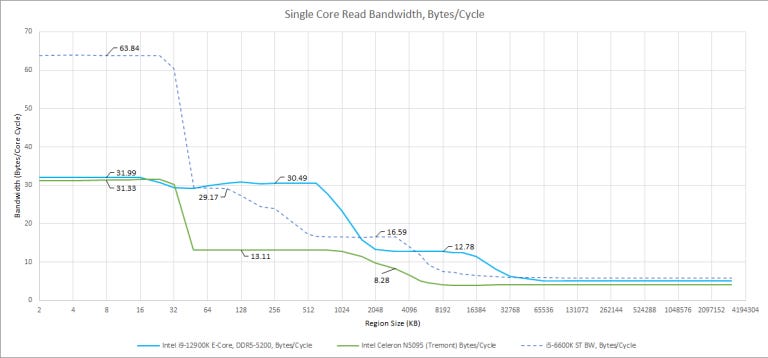
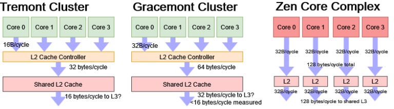
Unlike Gracemont’s L2, which could give 32B/cycle of bandwidth to a single core, Tremont’s cores only have a 16B/cycle L2 path. L3 bandwidth per clock is also abysmally poor and only mobile SoCs have worse bandwidth to their system level caches. For example, a Cortex A75 core on a Snapdragon 670 achieved 5.22 bytes per cycle in the SLC region. Here’s a comparison against other non-mobile chips with 128-bit datapaths:
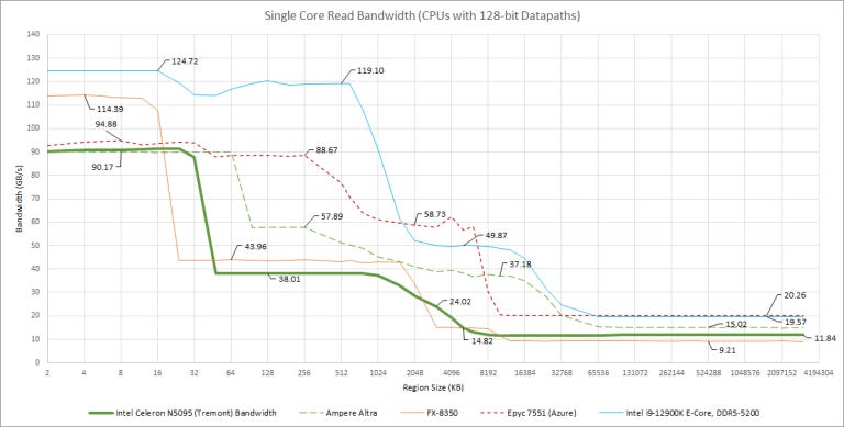
Most of the cores here can do two 128-bit loads every cycle from their L1 data caches, so differences are mostly down to clock speed and things get more interesting as we get to the L2 cache. Tremont has Piledriver-like L2 bandwidth characteristics, which isn’t great then things get worse as we hit L3. Bandwidth hungry vectorized workloads will feel great suffering, especially when multiple threads are in play:
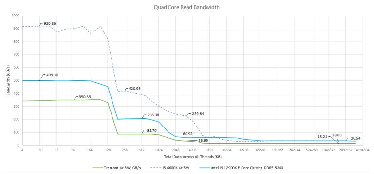
Bandwidth scaling is quite poor and with four threads, we only see a 55% increase in L3 bandwidth. Memory bandwidth scaling is even worse, likely because of the single channel DDR4 controller. If we graph bytes per cycle, a shared L2 bandwidth bottleneck shows up too:
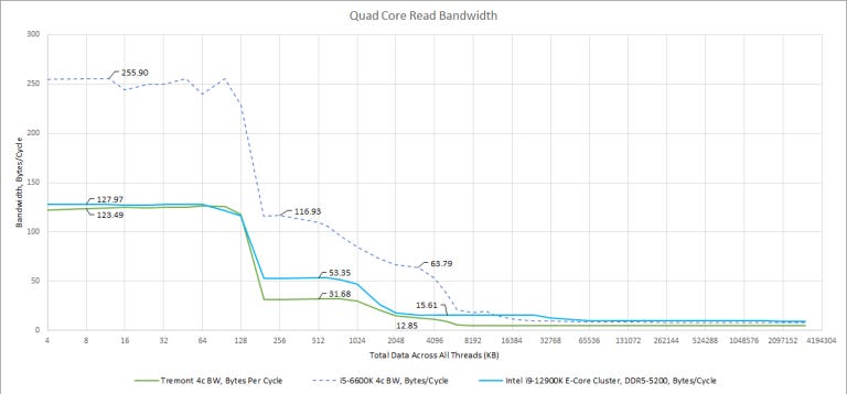
Tremont’s L2 paths are half the width of Gracemont’s. A single core can’t get more than 16 bytes per cycle from L2, and the whole L2 is limited to 32 bytes per cycle regardless of how many cores are loaded. Previously we thought Gracemont’s bandwidth looked weak, next to high performance desktop cores, but looking from Tremont’s perspective, it looks like Intel beefed up Gracemont’s cache bandwidth to let it do a passable job with vectorized workloads.
We’ve done more analysis of Tremont’s memory subsystem, but we have put it in the appendix to keep things short and sweet.
Different Targets for Atom
Intel’s own presentations also indicate ambitions beyond cell phones and tablets. For example, cache quality-of-service restrictions have no place in a single user client machine. But in the cloud, that’s often used to control each tenant’s share of cache capacity and bandwidth.
Tremont has ambitions beyond the cloud too. Intel’s presentation mentions 5G networking and Internet of Things as targets, and Tremont appears in Snow Ridge form for edge computing. And as we all know, Atom wound up on desktop too. In Lakefield, Tremont (and Sunny Cove) helped Intel figure out their heterogeneous core strategy.
Where Does Tremont Stand?
With those goals in mind, the Atom team implemented Total Memory Encryption to protect enterprise deployments from cold boot attacks. “Accelerator interfacing instructions” make the core better suited to working with offload devices like GPUs. And of course, Tremont needed to punch harder than previous Atoms to contribute on desktop CPUs. So Tremont gets big-core like branch prediction capabilities, reordering depth, and core width.
Still, this feels like a an architecture in transition: The all-important caches are weak, execution resources are a bit thin compared to big cores, the integer scheduler is small even compared to that of contemporary ARM CPUs like Neoverse N1 which can be a stumbling block that prevents Tremont from extracting as much instruction level parallelism as other equally wide cores. A smattering of Atom-style tradeoffs round out the picture, leaving Tremont in no man’s land. It’s significantly stronger than prior Atom architectures yet it stops short of approaching desktop CPUs in both performance per clock and clock speed.
But that’s not really a bad thing, because Tremont in Jasper Lake form still has excellent power consumption characteristics which really hits home with regards to what Intel wanted out of Tremont:
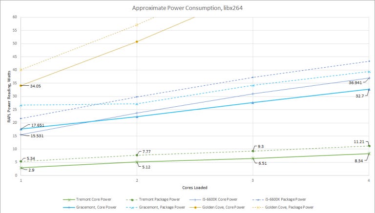
The Celeron N5095 absolutely sips power. When one core is loaded, it doesn’t suffer high power draw from shared components like Gracemont amd when the encoding job uses all four cores, each Tremont core draws just over 2 watts. Celeron also consumes very little non-core power; the package power was just 2-3 watts higher than core power, compared to over 6 watts of uncore power on Skylake (and Alder Lake).
With four cores active, Tremont, Skylake, and Gracemont encoded the video at 0.98, 2.01 and 1.97 FPS, respectively. Tremont was half as fast but draws around a quarter of the power, so it’s definitely more power efficient yet at the same time, a user would notice if the encoding job took twice as long, so it’s definitely a tradeoff.
Wrapping it Up
Tremont’s strengths:
4-wide core and 6-wide frontend mean plenty of potential throughput
High reordering capacity, especially for branches
Clever use of Zen style non-scheduling queues to reduce backend stalls
Fast branch predictor with reasonable accuracy
Low power consumption, excellent power efficiency
Well tuned for low clocks, with 3-cycle L1D access and low mispredict penalty
And its weaknesses:
Clustered decoder can get tripped up by huge unrolled loops
Small integer scheduler. Too small.
No AVX support hurts heterogenous core configurations
Poor memory subsystem – high latency and low bandwidth
Intel’s Tremont architecture is interesting not because of its absolute performance, but because it represents a change in Intel’s Atom strategy. At its start, Atom cores went into netbooks, tablets, and even cell phones and with those power and thermal restrictions, Intel’s engineers tried to give Atom adequate performance in everyday workloads. They optimized for the most common integer operations and made sacrifices everywhere else which meant that performance was medicore and fragile, and in turn, limiting Atom’s reach.
Tremont looks to change that. Intel announced Tremont in 2019, which means its development was underway in 2017 – about when Zen launched. Intel likely saw the threat posed by small, efficient cores. AMD and ARM could pack more cores into a socket and win in throughput bound loads, where Intel’s per-thread advantage would count for little. The phone effort went nowhere after a couple of generations, so Intel decided it was time to make the Atom line defend its own turf and by covering the low power, everyday use case, Atom potentially lets Intel’s big cores aim for higher performance by de-prioritizing the ability to scale down in power.
If you like our articles and journalism and you want to support us in our endeavors then consider heading over to our Patreon or our PayPal if you want to toss a few bucks our way; if you would like to talk with the Chips and Cheese staff and the people behind the scenes then consider joining our Discord.
Appendix
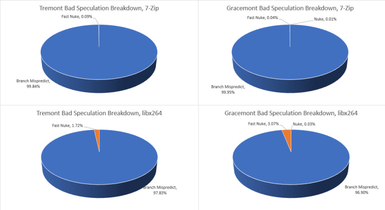
Bad Speculation Causes
Retirement Bandwidth
We didn’t directly measure Tremont’s retirement bandwidth, nor could we find anything Intel said on the matter. So, we simply programmed counters with the instructions retired event (event 0xC0, umask 0) with different count masks. We always got zero counts when the count mask was over 4, indicating that Tremont never retired more than 4 instructions in one cycle.
Undocumented Counters on Skylake
For backend resource stalls, we wanted to make the best comparison we could to Skylake. But Intel doesn’t document any performance monitoring events for Skylake’s register files filling up. However, Sandy Bridge documents a couple interesting events:

Since Intel’s descriptions are about as useful as a math textbook (where tradition demands that symbols used are never defined), we used our structure size benchmarks to figure out what the events actually count. Unit masks in performance monitoring events are used to select a more specific sub category. For example, a hypothetical event could monitor the number of users that access a drink machine. Then, unit masks could restrict counting to just users that choose apple juice, or orange juice. The unit mask is usually a bitmask, meaning that setting a bit to 1 selects a sub-category.
When we use a test that bottlenecks on register file capacity, we see high counts from the ALL_FL_EMPTY event regardless of whether we test using floating point or integer registers. The unit mask of 0xC, or 1100 in binary, suspiciously means two bits are set. If we individually set those bits, we get high counts with the fourth bit if the FP register file is hit. And high counts with the third bit set if we hit the integer register file. The first bit produces high counts with a test that hits both register files. We repeated these tests on Skylake to make sure the event still works there, even though it’s undocumented.
In summary, here’s how we think the event works on Skylake:

To estimate how often Skylake couldn’t send a micro-op to the backend because no registers were available for renaming, we added up the counts for bits 1, 3, and 4.
But please treat our figures as rough estimates. Performance counters measure awfully specific things and similar counters can have slightly different meanings on different architectures. And using undocumented counters means we have zero guarantees about counter accuracy, even if we’ve done basic validation to see if the counters work. We’re providing the figures in the article to give a rough idea of where bottlenecks are.
Extended Memory Subsystem Analysis: Write Bandwidth
Writes are similar to reads, though bandwidth is generally lower. That’s understandable, since CPUs typically execute far more reads than writes. Tremont can only do a single 128-bit store per cycle. Gracemont has matched load and store bandwidth, at least to the L1 data cache. It’s pretty impressive for an efficiency oriented core like Gracemont to match Skylake’s store bandwidth.
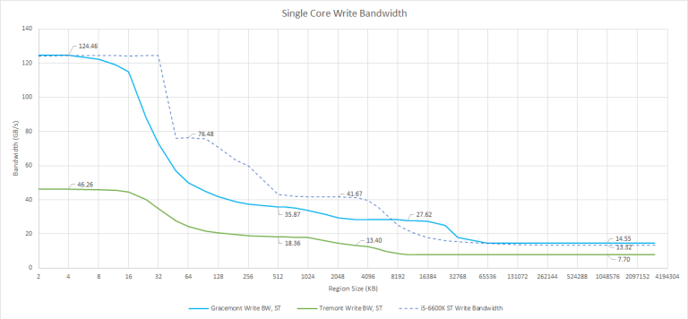
However, once we get into lower cache levels, Skylake takes a clear lead. Just like we saw with reads, Skylake is a big core designed for high bandwidth. While Alder Lake’s L3 can provide plenty of bandwidth to big cores, Gracemont is unable to take full advantage of it. In DRAM sized regions, Gracemont pulls ahead even with a single core. Since the core doesn’t need to wait for data from the memory subsystem to complete a write, this test is less sensitive to DDR5’s high latency. Tremont, in Jasper Lake form, suffers in all areas. It simply doesn’t have a memory subsystem optimized for high bandwidth.
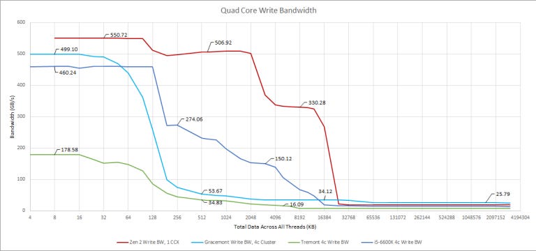
The pattern is similar when we hit more cores. Gracemont gets a slight lead against the i5-6600K in L1D regions by holding 3.8 GHz when four cores are loaded, while the Skylake i5 drops to 3.6 GHz. Tremont sees some scaling L2 write bandwidth scaling from more threads. But L3 write bandwidth doesn’t really scale, and overall performance remains poor.
Store to Load Forwarding
Pipelined CPUs have to deal with memory dependencies. Before executing any load, it has to figure out whether to get the data from a previous in-flight store, or directly talk to the memory subsystem. When a store’s data is sent to a later load, that’s called store forwarding. But that process isn’t as simple as seeing if a load’s address is equal to that of a prior store. Stores might only partially overlap with a load. Or a store might totally contain a smaller load, even if their addresses don’t match. Henry Wong has a more thorough explanation of this, along with a batch of test results, so let’s jump right into what Tremont does:
Tremont’s store forwarding only works if the load’s address is aligned with the store, with respect to the load size. That is, a 64-bit store’s upper or lower half can be forwarded to a subsequent 32-bit load. All other cases fail, including ones where the load is completely contained within the store. If store forwarding succeeds, it takes five cycles for the load to get a result. Failed store forwarding costs 11-12 cycles. If either the load or a store crosses a cache line boundary, store forwarding always fails, and another penalty cycle gets added.
That’s a significantly weaker showing than Skylake, where store forwarding always succeeds if a load is contained within a larger store. Latency is two cycles higher if the load crosses a cache line, but that’s much better than outright failing and taking 12-13 cycles like Tremont.
Perhaps the best comparison is Neoverse N1, as implemented in Ampere Altra. Like Tremont, N1 can only forward either the upper or lower half of a 64-bit store to a 32-bit load. Forwarding latency seems slightly longer, but N1’s forwarding mechanism continues to work across a 64 byte cacheline boundary.
Neoverse N1 and Tremont both make similar tradeoffs in their load/store units, which is fascinating. Both of those architectures emphasize low power over absolute performance, and that involves all kinds of minor tradeoffs not visible in a block diagram or marketing presentation.