
Nvidia’s Ampere & Process Technology: Sunk by Samsung?
While chronic GPU shortages dominate the current news cycle (exacerbated by a myriad of individual factors set to continue for the foreseeable future), the massive increase in power requirements for high-end graphics cards is just as newsworthy. These higher-power GPUs don’t just raise your power bill; they can require a PSU upgrade or exhaust a large amount of heat into your room while in use.
AMD remained at a roughly 300w power target in the high-end market when it transitioned from its Vega 10 GPU to Vega 20 and then Navi 21. Nvidia’s GA102 chip that powers the RTX 3080 and 3090 is able to draw up to 350w at stock, and north of 400w in some factory-overclocked models. While this has given AMD a slight, yet noticeable, advantage in power efficiency over Nvidia for the first time in ten years—having last held this distinction with the Cayman GPU powering the HD 6900 series of graphics cards—some have pointed fingers at Samsung’s 8N process technology as the root of Ampere’s struggles and argued that Nvidia’s architecture would be clearly superior to AMD’s if AMD did not possess a substantial process advantage. TSMC’s N7 process is indeed better in some respects than the Samsung node used by Nvidia, yet the facts clearly show that issues with the Ampere architecture run far deeper than just the choice of process technology, and that AMD’s architectural merits are not to be dismissed merely as a node advantage.
Samsung 8N: Just a Renamed 10nm?
Samsung’s 8N process, a development of its commercial 8LPU process, has come under fire from some commentators who argue that it is merely a refreshed 10nm-class node and not in the same tier as TSMC’s 7nm nodes. While 8N is indeed a development of the Samsung 10LPE node, it is important to understand that Samsung values much more gradual jumps in process density and performance than some of its competitors. This mitigates risk and will often achieve values very close to a “new” node. Samsung can safely and economically improve older nodes by backporting technologies and features from newer nodes. For example, their 11LPP node (technically a development of a 14nm-class process) uses a 10nm backend-of-the-line (BEOL) as well as new libraries that provide a substantial increase in density very close to a “true” 10nm-class node.1 According to Samsung, 11LPP offers a 15% performance improvement or 42% lower power at the same performance, as well as a theoretical 57% density increase when used with the new 6.75T libraries.
Therefore, while not quite as performant as “name-brand” 10nm, 11LPE is extremely close in density and performance characteristics, and therefore warrants its branding as being closer to 10nm than 14nm.
A similar situation is present with the 8LPU node on which 8N is based. Samsung planned to introduce EUV lithography on their mainstream 7nm node, unlike competitor TSMC which first created a DUV-based 7nm node and then introduced EUV as a sub-node. (The first mainstream TSMC process node to use EUV lithography was N5, which entered full production in 2020 and is primarily utilized by Apple at the time of writing.) Therefore, Samsung wanted to develop their 10nm technology as close to 7nm as possible. It aided them in the EUV transition and provided an option for customers uninterested in EUV-based nodes. “8nm” was created explicitly as a stopgap between 10nm and 7nm rather than just being a refreshed 10nm, according to Samsung principal engineer Hwasung Rhee.2 Like TSMC’s DUV-based N7 node, it is intended as a long-lived node and the best non-EUV node that Samsung offers, with at least a 15% density improvement. 8LPU offers further performance improvements over 8LPP for high-performance computing through the use of a new uLVT library.3
A Mobile Comparison
As neither AMD nor Nvidia have released gaming-focused GPUs this generation on both Samsung and TSMC nodes with identical or even similar architectures, the closest apples-to-apples comparison of Samsung 8LPU and TSMC N7 will be in the mobile arena. Both Samsung’s Exynos 9820 and Huawei’s Kirin 980 smartphone SoCs use almost identical ARM Mali G76 GPUs, but the Samsung chip is built on 8LPU and the Huawei chip on N7. In the GFXBench Manhattan 3.1 benchmark, the Exynos chip actually displays superior performance-per-watt to the Kirin despite using the same GPU and is within spitting distance of the Snapdragon 855, also built on TSMC N7.4 The Exynos 9820 is also significantly ahead of Samsung’s previous Exynos 9810 chip, built on the 10LPP process. While some of this is undoubtedly attributable to architecture, the Exynos series is not considered to have leadership performance in most areas and yet is still able to provide comparable performance-per-watt to the competition on the 8LPP process. As the Exynos 9820 does not use 8LPU and the further advancements that it brings, these numbers are likely a conservative lower limit for competitiveness, rather than an upper bound.
Before continuing, it is important to note that this does not mean Samsung 8LPU is necessarily better than or even equal to TSMC N7 and its derivatives. TSMC’s process is ahead in several key metrics, especially fin pitch, and is by all accounts the better node for most use cases. However, the assertion that products built on 8LPU must be a full-node or even a half-node behind those built on N7 simply does not hold up to scrutiny.
Comparing Density: AMD vs. Nvidia
When Nvidia’s gargantuan A100 HPC accelerator was revealed in May 2020, many were amazed at both the sheer number of transistors comprising the chip and the transistor density which Nvidia and TSMC achieved. Despite being built on the same N7 process, Nvidia managed a transistor density more than 50% higher than AMD’s Navi 10 GPU. When the consumer-focused Ampere GPUs released later in the year with density figures more similar to AMD’s GPUs, some took this as proof of Samsung’s inferiority; Nvidia was achieving drastically higher densities with TSMC vs. Samsung, and the node performance must have been much worse with Samsung as well, hence the inflated TDPs. In order to understand why this is mistaken, it will be helpful to consult the following table:

The release of AMD’s MI100 GPU, built on the same node as A100 and serving as its direct competitor, clarifies the situation. Both of these GPUs run at considerably lower clock speeds than gaming GPUs and are therefore able to achieve much higher density. In the case of A100, this was especially important due to the necessity of remaining under TSMC’s reticle limit (858mm2), which likely necessitated some additional design compromises. AMD was nowhere near the reticle limit with their HPC GPU, but still achieved higher transistor density than Nvidia on the same node, demonstrating that their physical design capabilities are about equal. Nvidia achieved a slightly higher transistor density with Ampere than AMD’s Navi 10 at similar clockspeeds (roughly 1800–1900 MHz in standard workloads), but AMD leapt ahead by a similar margin with their RDNA2 GPUs.
What explains RDNA2’s transistor density despite targeting far higher clockspeeds (2300–2600 MHz) than either Ampere or Navi 10? One answer would be the introduction of AMD’s Infinity Cache technology. By placing a large amount of SRAM on-die, AMD is able to use a smaller memory bus on their high-end GPU than Nvidia requires (256-bit vs. 384-bit). Memory controllers occupy substantial area on-die and typically do not shrink as well as logic with successive advancements in process technology. In contrast, TSMC’s N7 is renowned for its exceptional SRAM density, an advantage which AMD has fully utilized in both Zen 2 and RDNA2.5
Samsung Nodes: Good for Mobile Only?
One persistent truism is that Samsung’s process nodes are mostly targeted at mobile SoCs and do not work well for high-performance computing use cases such as gaming GPUs. In order to check the validity of this claim, it is worth reviewing Nvidia’s Pascal architecture from 2016, which was dual-sourced on TSMC’s N16 and Samsung’s 14LPP nodes depending on the individual chip. The GTX 1050 Ti, based on the GP107 GPU fabricated by Samsung, typically operates at around 1715 MHz in a gaming workload.6 For comparison, the GTX 1060, based on the GP106 GPU fabricated by TSMC, regularly operates in the 1840 MHz range.7 While this would seem to be a significant disadvantage for Samsung, the GTX 1050 Ti operates without a PCIe power connector and regularly hits a hard limit of 75w power consumption, placing a cap on attainable clockspeeds; the GTX 1060 can draw substantially more power and therefore boost higher. This is reflected in a performance-per-watt comparison, where the GTX 1050 Ti is almost 10% more efficient than the 1060 as a result of the power cap.8 Despite some design and competitive differences between the two nodes, the proximity of these two GPUs in key metrics like power and clock speeds shows that the two process nodes are at least in the same class for gaming GPU use cases. It is also worth noting, of course, that AMD used the 14LPP process licensed to GlobalFoundries for its highly acclaimed Ryzen 1000 “Summit Ridge”, Threadripper 1000 “Whitehaven”, and Epyc “Naples” processors, all of which featured excellent performance and power figures in a high-clockspeed HPC environment.
Clockspeed Superiority: Not Just the Node
One aspect of the 2020 generation of graphics cards that has fueled perceptions of a node imbalance has been the sky-high clockspeeds that AMD has achieved with its RDNA2 architecture. Since AMD released its Graphics Core Next architecture in 2011, Nvidia has generally achieved higher clockspeeds on the same process node. This first became extremely apparent with Nvidia’s superlative Maxwell architecture, whose enormous GM200 top-of-the-line GPU was easily overclockable to over 1300 MHz in most operations.9 AMD’s competing Fiji GPU, marketed as “an overclocker’s dream”, was only able to achieve a little over 1100 MHz despite its similar proportions to GM200.10 This gap widened during the FinFET generation, with the aforementioned GTX 1060 easily reaching 1830 MHz while the comparable Polaris 10-powered RX 480 hovered around 1250 MHz on average at similar voltages.11 It might be reasonable to conclude that, should this trend continue, Nvidia would easily reach upwards of 2300–2500 MHz on TSMC 7nm, outpacing AMD as they have generally done for the last decade.
However, it should be apparent that clockspeed is not merely determined by the process node—with smaller transistors able to switch faster at a lower voltage—but also by physical design. One possible method for improving performance on the same process node is by working more directly with the fabrication process itself—what is generally known today as design technology co-optimization (DTCO). By leveraging transistor-level optimizations on the 28nm node, Nvidia was able to significantly improve both maximum frequency and power efficiency with its Maxwell architecture without a node improvement.12 Another method is path optimization—essentially identifying slow portions of the design and optimizing them so that the entire chip can operate at a higher frequency. This was what Nvidia leveraged with their Pascal architecture alongside FinFET transistors, and was why Nvidia achieved nearly 45% higher clockspeeds while AMD’s Polaris saw less than a 20% improvement in the same generation.13

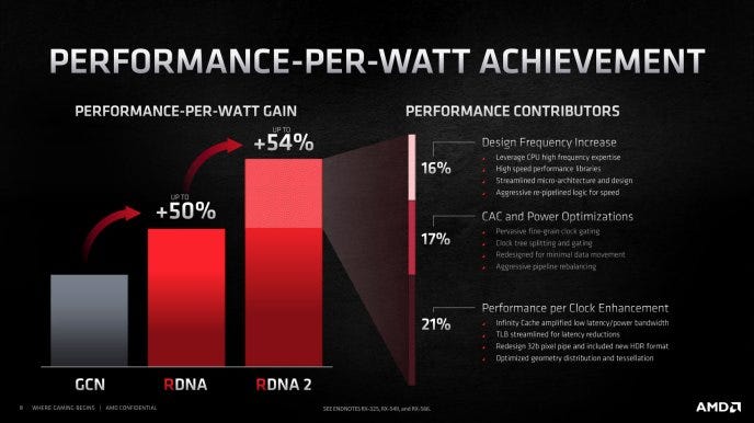
With its RDNA2 architecture, AMD leveraged two years’ worth of design experience with both CPUs and GPUs manufactured on the TSMC N7 node to provide substantial efficiency and performance improvements. AMD occupies a unique position due to its willingness to utilize cutting-edge process nodes very early in their lifetime (the large Vega 20 GPU was released only a few months after N7 began mass production) and the resulting wealth of experience it has with the N7 node in particular (RDNA2 is AMD’s third-generation 7nm GPU family). AMD can also take advantage of advancements by its CPU team when designing its GPUs, an advantage that few other companies possess. One of the best examples of this cross-pollination is AMD’s Infinity Cache technology, which was made possible by leveraging the design of the L3 cache found in EPYC processors. In addition, AMD specifically cited its high-frequency CPU design expertise as one source of the frequency increase they were able to achieve with RDNA2.
Now that AMD is sharing this design expertise across all divisions, it will not be as straightforward for Nvidia to achieve similar or higher frequency with their designs, especially when they have far less experience with a node than AMD does. As another reminder that 7nm is not an automatic path to high clockspeed without an equally tuned architecture, AMD’s Radeon VII based on the Vega 20 GPU only achieves an average frequency of 1775 MHz in a gaming workload, still lower than the 1830 MHz of 16nm-based Pascal GPUs.14
Ampere on N7: A Historical Parallel
In order to predict what might occur in a hypothetical situation where Nvidia shrunk Ampere to 7nm on TSMC’s process, we can review a similar situation from 2009 with several parallels to today. In the 2008 graphics card market, Nvidia’s top-of-the-line product was the GTX 280 powered by the GT200 GPU, produced on TSMC’s 65nm process and weighing in at a massive 576mm2. AMD’s highest-end competitor, the Radeon HD 4870, was powered by the 55nm RV770 GPU with a die size of only 255mm2 and was within 15% of the GTX 280’s performance while enjoying equal or slightly superior power efficiency.15 The smaller die size also allowed AMD to sell their cards far more cheaply than Nvidia. About eight months after the release of the GTX 280, Nvidia took advantage of the 55nm node themselves and shrunk the GT200 GPU to create the GT200B at a much more manageable size of 470mm2; this GPU powered the GTX 285. One might expect Nvidia to suddenly hold a large performance and efficiency lead, given that they were slightly behind or equal to AMD’s 55nm GPUs while on the less-advanced 65nm node. However, the GTX 285 only achieved a 5% performance increase over the GTX 280, and power efficiency was increased by a mere 10%.16 17 Despite GT200B only being around 81% of the size of GT200, it did not provide performance improvements in line with that figure. This is attributable to several factors but, in particular, die shrinks of an older architecture are almost never as effective as architectures specifically designed from the outset to use a newer node.
However, what is most important to take away from this example is that the 55nm die shrink did not substantially change the competitive field. AMD responded with a slight revision of their RV770 GPU that allowed it to reach higher clockspeeds and achieve slightly better efficiency, and this refreshed GPU was actually closer to the performance of the GTX 285 than the original was to the GTX 280.18 Therefore, if Nvidia were to shrink Ampere to the exact same node that AMD presently uses, and 8LPU has been demonstrated to be at least as close to TSMC’s N7 as 65nm was to 55nm—if not closer—it is reasonable to conclude that it, too, would not significantly change the competitive landscape.
Tracing Ampere’s Efficiency Issues
If Samsung’s process node is not wholly to blame for the higher power consumption of Ampere GPUs, then what is? The first, and perhaps most obvious, reason would be that Ampere is simply an inefficient or flawed architecture for gaming workloads. This has happened before with the Fermi architecture powering GTX 400 and 500 graphics cards; while AMD achieved a nearly 80% uplift in performance-per-watt moving from 55nm to 40nm, Nvidia’s performance-per-watt with the GTX 480 was worse than 65nm chips, let alone 55nm chips.19 This occurred in spite of a 40nm node shrink, new GDDR5 memory technology, and a radically re-designed architecture. The “fixed” refresh of the GTX 480, the GTX 580, was around 15% more efficient than the 480 but was still only equal to 55nm cards like the GTX 285.20 Nobody would believe that TSMC’s 40nm process was at fault for the lack-lustre efficiency of the Fermi architecture, especially in comparison to the gains of its competitors. Rather, the poor efficiency resulted from architectural choices like the double-pumped shader array that were reversed in the far more efficient Kepler architecture that followed.
One culprit for Ampere’s power usage may be its GDDR6X memory. Nvidia has traditionally shied away from using HBM in its consumer GPUs due to the extra packaging expenses, and has stuck with GDDR memory technology instead. However, the TU102 GPU behind the RTX 2080 Ti and Titan RTX already used a 384-bit 14 Gbit GDDR6 memory bus, leaving little room to expand without using an unproven 512-bit memory interface that had not been seen since 2013 and which would have led to further signalling and routing issues. Ampere is a particularly bandwidth-hungry architecture due to its high CUDA core count (like similar past architectures such as Vega), and 16 Gbit GDDR6 on a 384-bit bus would not have provided enough bandwidth for the GA102 GPU. Nvidia was forced to look elsewhere for a solution.
That solution was provided by Micron’s GDDR6X technology, a cutting-edge addition to GDDR6 that incorporates PAM4 signalling to drive much higher bandwidth from a similarly-sized memory interface. However, incorporating this technology has imposed a heavy power cost, likely due to the additional complexity of PAM4 signalling for the memory controller. This power cost can be clearly seen in the RTX 3070 Ti, which features a 70w higher TDP than the 3070 despite the only real difference being a switch to GDDR6X memory. AMD chose a different approach with its RDNA2 GPUs, foregoing next-generation memory technology in favour of a large L3 cache on-die. It is estimated by Chips and Cheese that the Infinity Cache on Navi 21 GPUs comprises 6.144 billion transistors and a die area of 135mm2, or nearly 25% of the total die area. This solution has upsides and downsides, but it has allowed AMD to avoid paying the heavy power cost of GDDR6X and allowed it to use a substantially smaller memory bus.
Another potential source of its power efficiency issues would be the large number of CUDA cores intrinsic to the design. With Ampere, Nvidia converted their separate integer pipeline added in Turing to a combined floating point/integer pipeline, essentially doubling the number of FP units per streaming multiprocessor. While this did result in a potential performance uplift of around 30% per SM, it also presents challenges for keeping the large number of cores occupied.21 Ampere has been shown to exhibit lower shader utilization and more uneven workload distribution when compared to the earlier Pascal architecture.22 These issues with occupancy resulting from a large core count are ones Ampere shares with other high core-count and power-hungry architectures such as Vega; like Vega, Ampere appears to be a better fit for compute-heavy workloads than many gaming workloads.
Implications for the Future
If there is one lesson that this article has hopefully hammered home, it is that process technology is not an instant fix to a bad architecture. By investing heavily in architecture design, Nvidia enjoyed a substantial performance and efficiency advantage over AMD that sometimes amounted to a full node shrink. It is possible that Nvidia will be able to re-take the efficiency crown in the future through this same process. However, a mere switch from Samsung to TSMC would not necessarily be enough to outweigh the downsides of a flawed architecture. If both AMD and Nvidia shrink their present architectures to 5nm, AMD could very well come out on top for a second time. It remains to be seen if Nvidia will truly fix Ampere’s flaws in the next generation or if they will rely on features like DLSS and a superior real-time raytracing implementation in order to drive sales.