The Nerfed FPU in PS5’s Zen 2 Cores
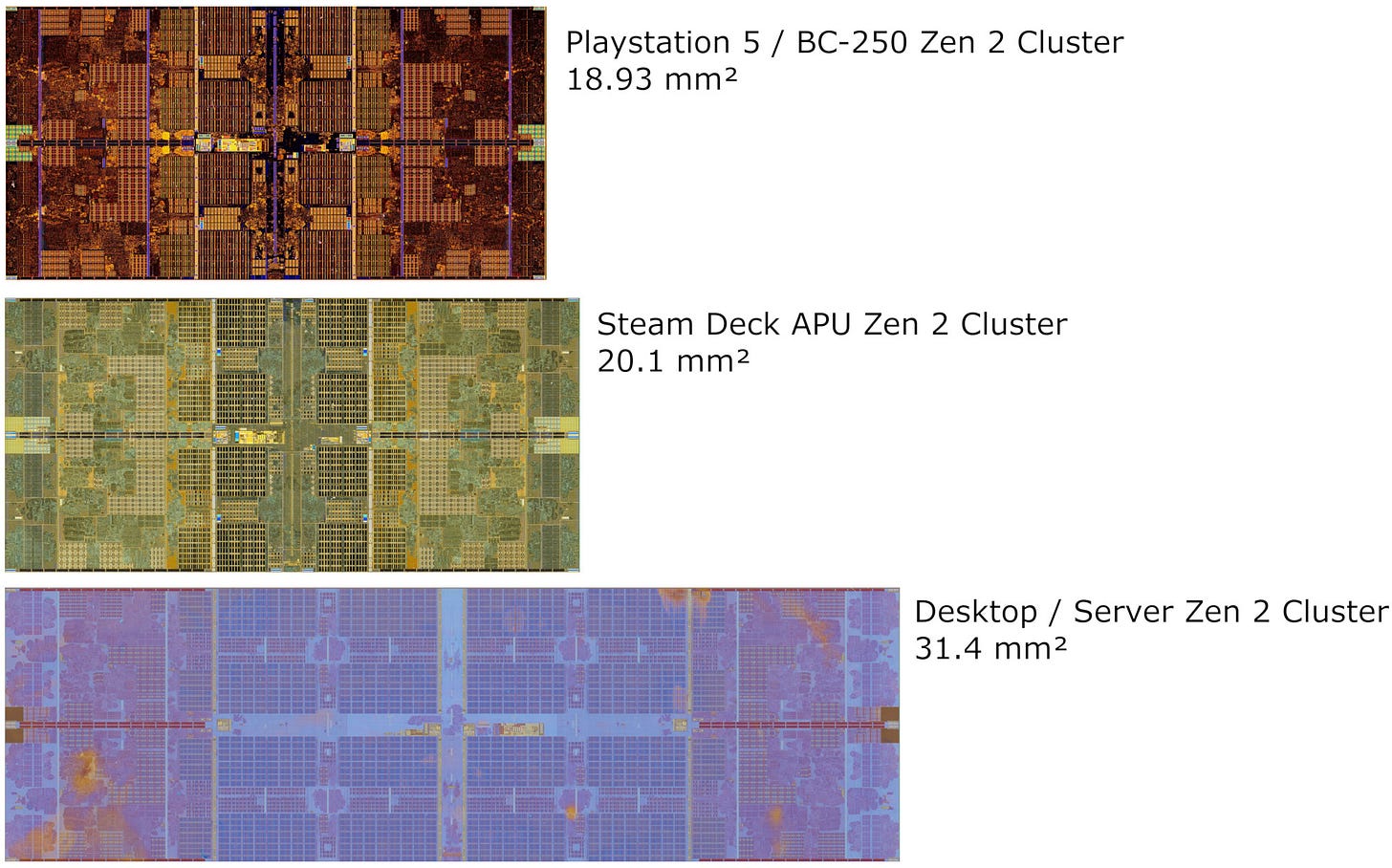
Fritzchens Fritz’s awesome die photos revealed that the Playstation 5’s Zen 2 cores spend less die area on their FPUs than their desktop cousins. Thanks to Brutus, I got to take a closer look at just how AMD got Zen 2’s FPU to drop from 0.91 to 0.59 mm2. Brutus specifically acquired and gave me access to AMD’s BC-250. The BC-250 uses a harvested PS5 chip with six enabled Zen 2 cores and a very cut down GPU, and is supposed to be used for crypto mining. That means I get access to the same PS5 style Zen 2 cores, and can target them with microbenchmarks and performance counters.
For this article, I’ll be referring to the BC-250’s Zen 2 cores as PS5 Zen 2 cores. It’s a lot easier to say PS5.
Overview
The FPU on the PS5’s Zen 2 cores occupies the same width along the short side of the core, but look very compressed on the other axis. There’s a lot less blank area, and less area looks allocated to the execution units on either side too.
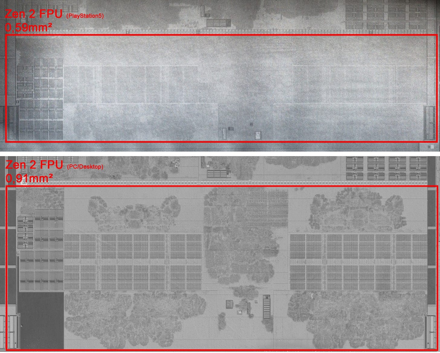
But AMD didn’t get this area reduction for free. Instead, they cut down the FP pipes and eliminated some duplicate FP/vector execution units. Zen 2 nominally has a quad port FPU, with ports named FP0, FP1, FP2, and FP3. On the PS5, FP3 has been deleted. FP2 is relegated to only handling FP/vector stores, with all of its math execution units removed or moved to FP0/FP1. Long story short, AMD did this:
With those changes, the PS5’s Zen 2 cores effectively have a dual port FPU with the ability to co-issue stores. But the execution units weren’t the only things to shrink in Fritzchens Fritz’s images. The register file in the center is visibly changed as well. While it’s divided into the same number of blocks, the blocks are both closer together and smaller.
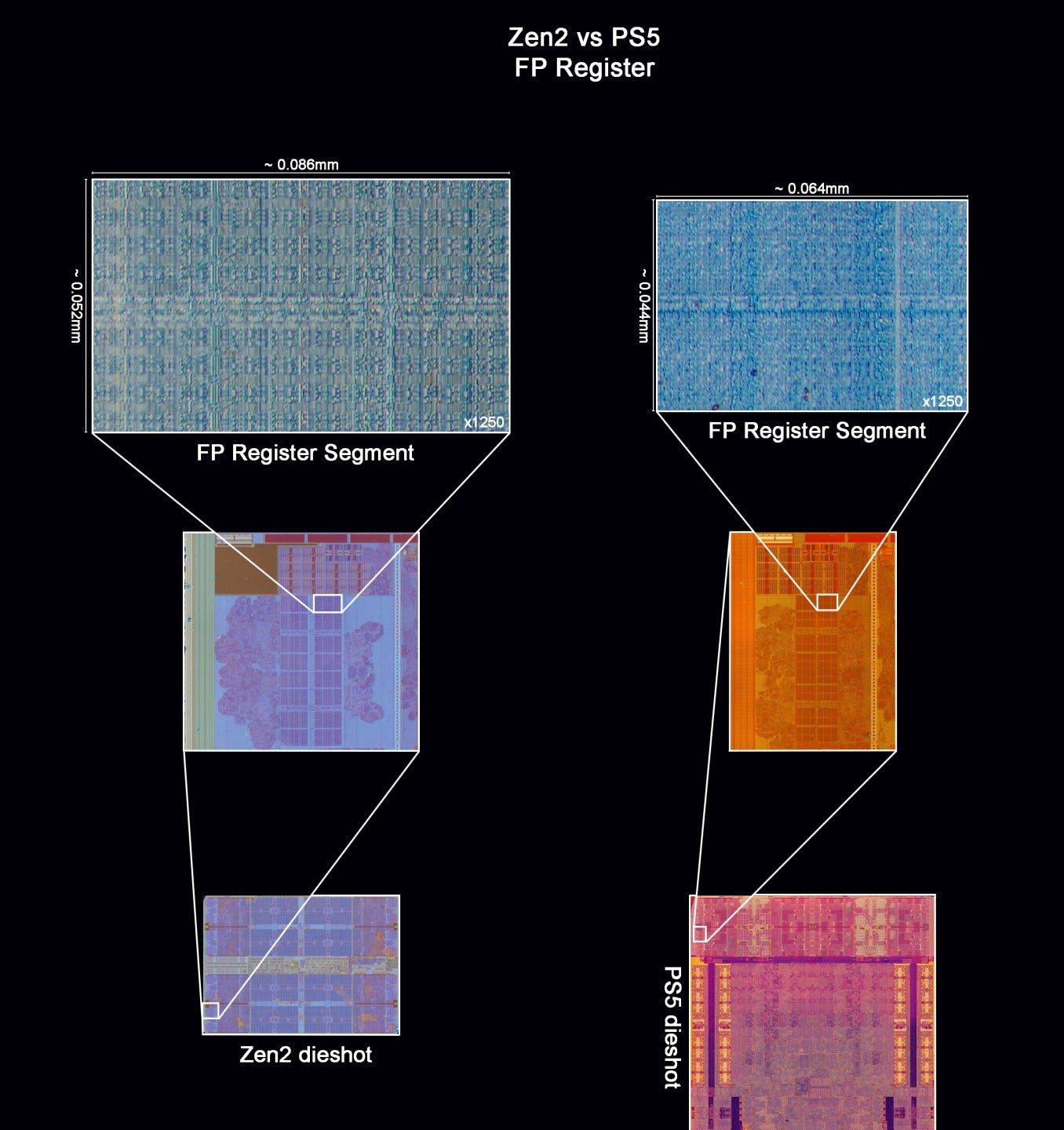
However, microbenchmarking speculative FP/vector register file capacity indicates the PS5’s FPU continues to have Zen 2’s full 160 entry register file. Using 256-bit FP adds as filler instructions produces a similar result, so each entry is still 256 bits wide.
I suspect AMD was able to make the register file smaller because they could make do with less register bandwidth after cutting down the execution pipes. AMD noted register file area was more dependent on port count and width than capacity.
And even the physical register file, which can now hold 512-bit registers, had only minimal growth since register file area is mostly limited by the width and number of access ports, and not so much the number of storage cells per entry.
While they made that observation for Zen 4’s AVX-512 implementation, it’s likely equally valid for the PS5’s cut down Zen 2 FPU. Many of AMD’s FPU modifications mean the register file can feed the execution pipes with fewer ports.
Feeding Zen 2’s four execution pipes could require up to 10 inputs, but AMD’s optimization manual says FP3’s source buses are reused to provide a third input for the FMA units on FP0 and FP1. I interpret this to mean Zen 2’s register file only had eight ports to help keep register file area under control. Zen 2 PS5 edition would only need six register read ports to feed its FP pipes, further cutting down register file area.

The PS5’s cut down FPU would have 192 and 128 bytes per cycle of read and write bandwidth respectively, or 672 GB/s read and 448 GB/s write at 3.5 GHz. For comparison, Zen 2 has 256 and 192 bytes per cycle of read and write bandwidth. At 3.5 GHz, that would be 896 GB/s of read bandwidth, and 672 GB/s of write bandwidth.
AMD also left the scheduler and non-scheduling queue (NSQ) intact. Therefore, the FPU’s all-important latency hiding capabilities remain unchanged. Performance counters (count mask = 4 on the FP pipe assignment event) indicate the scheduler or NSQ can still accept four micro-ops per cycle from the renamer. So, the FP renamer hasn’t been cut down either.

Zen 4 uses a similar strategy having less execution throughput paired with full-fat out-of-order structures to hide latency and keep it fed. We saw that strategy play out quite nicely, with Zen 4 getting a very decent performance uplift from AVX-512 despite having similar vector execution throughput to Zen 3.
But how that works out for Zen 2 is an interesting question. Cutting down execution hardware past a certain point can really hurt performance, just as going for an bargain basement GPU can drop you off a performance cliff.
Did We Need Those Pipes Anyway?
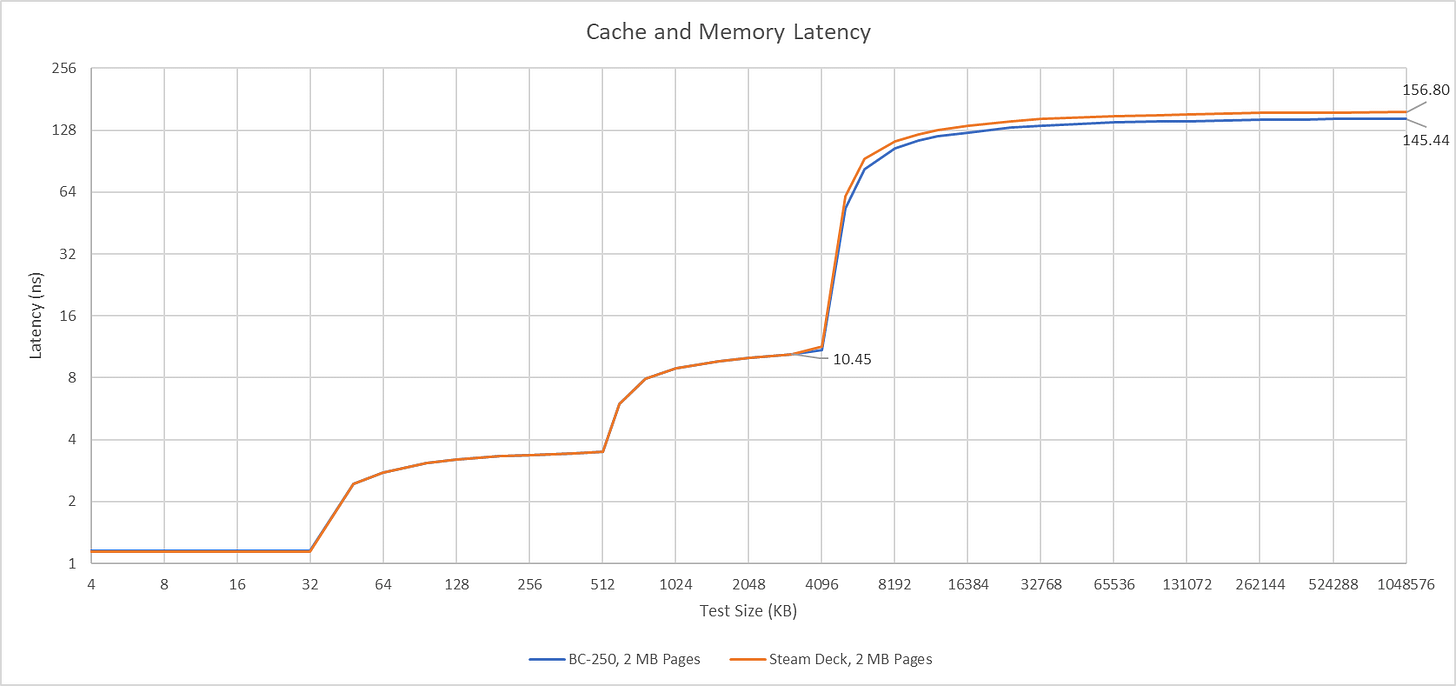
Unfortunately, there’s no way to get Zen 2 cores with cut down FPUs outside Sony’s custom APU, making comparisons difficult. But the Steam Deck’s APU comes close. Both have clock speeds capped to 3.5 GHz and 4 MB of L3 cache per cluster. LPDDR5 also approximates GDDR6’s horrible latency, though LPDDR5 is slightly worse.
However, there’s still a large bandwidth gap. CPU bandwidth on the Steam Deck is limited by the on-chip fabric. Meanwhile, the PS5’s CPU cores enjoy the highest DRAM bandwidth available to any Zen 2 implementation. I fell just short of 100 GB/s using a read-modify-write pattern with a 1 GB test array. If each cluster has a 32 byte per cycle read and write links to Infinity Fabric, the BC-250 probably has an Infinity Fabric clock of around 1.2 GHz.

Since bandwidth issues typically surface when a lot of cores are active, I’m locking benchmarks to three cores. I’m hoping the Steam Deck still has enough bandwidth to feed three cores in a single CCX. Using 3 cores in one CCX also creates the closest match between the two chips.
Both the Steam Deck and BC-250 were set up with Ubuntu Linux.
Setting a Baseline
7-Zip is a file compression program that’s heavy on scalar integer operations, but basically doesn’t touch the FPU. At the same time, its memory footprint is large enough to spill out of cache. That makes it a good test to set a baseline with.
The BC-250 is 4% faster. Memory latency is its biggest advantage over the Steam Deck’s APU, so that’s probably responsible for its lead. If the two chips end up within that margin in another test, I’ll call it a wash.
Moderate Vector Workloads: libx264 and SSIM
libx264 is a popular video codec, and still your only choice if you want embedded videos to play in Discord. Here, I’m transcoding a 4K Overwatch play of the game clip.
The Steam Deck APU pulls ahead by 14.9%. Zen 2 provides a performance monitoring event that counts micro-ops bound to each FP pipe, at the rename stage. Technically this event is undocumented in Zen 2, but I’ve tested it and it appears to work as expected. Furthermore, Linux’s perf utility still supports it.
Load from libx264 is evenly spread across Zen 2’s FP pipes, and no pipe stands out as an overloaded bottleneck. On the PS5’s nerfed FPU, load is shifted off FP2 and FP3 onto the first two pipes. They see higher utilization, but it’s not high enough to indicate a consistent bottleneck.
Out of order CPUs can smooth out spikes in demand for execution unit throughput by temporarily buffering more micro-ops in the backend while the execution pipes work to clear older ones out. But backend structures have limited capacity. If they fill, we can infer that a spike in demand or long latency operation exceeded the out of order engine’s capability to hide it, and thus caused a performance impact. Zen 2’s performance counters can tell us when this happened and pin down why. I’ll focus on the FPU’s register file and scheduler here.
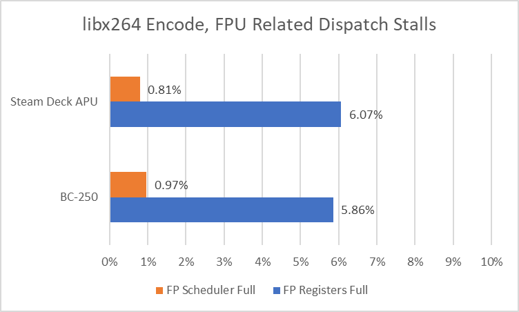
The FP scheduler will fill if too many FPU operations are waiting to be executed. That can happen because the FP pipes aren’t keeping up, or because there’s a long dependency chain. To be specific, a dispatch stall due to lack of scheduler resources happens when both the scheduler and non-scheduling queue are full. For simplicity, I’ll keep referring to it as a stall due to the FP scheduler filling, but remember that the combined 100 micro-op capacity of both structures have to be used before such a stall will happen.
Instructions that write to a FP or vector register also need a physical register allocated. If no entries are available, we get a dispatch stall too. Running out of space in the FP/vector register file doesn’t imply an execution bottleneck. But it does suggest some instructions that write to FP/vector registers are suffering from long latency.
Both Zen 2 variants are closely matched in terms of how often the renamer stalls due to a full FP register file or scheduler, which makes explaining the performance discrepancy difficult. The scheduler rarely fills, so steady-state execution throughput isn’t a bottleneck on either core. But the register file does, so long latency instructions are blocking retirement. My theory is that vanilla Zen 2 is able to clear out pending FP operations faster once that long latency instruction completes. In turn, that allows any FP micro-ops backed up into the non-scheduling queue to get into the scheduler faster. Because the FPU can only “see” in the 36 entry scheduler queue to extract instruction level parallelism, that lets normal Zen 2 feed its FP pipes more effectively.
My biggest takeaway from performance counters is that cut down Zen 2 would be a lot worse off if AMD decided to cut register file capacity in addition to nerfing the execution pipes. The register file is already a very hot structure, and making it less capable could drastically affect performance.
SSIM
Structural Similarity (SSIM) is a video quality metric. Calculating it also puts load on the FPU. The BC-250 and Steam Deck perform almost identically, with the Steam Deck ahead by 0.45%.
SSIM puts roughly even load on Zen 2’s four FP pipes, but FP2 does end up with more work. On the PS5’s nerfed FPU, more micro-ops are chucked onto FP0 and FP1 as expected, but FP2 gets a decent amount of work too. SSIM seems to be writing a lot of vector register contents to memory, which means the FP2 pipe is well leveraged.
Dispatch stall counters indicate the out-of-order engine is largely able to smooth out spikes in demand for the floating point execution units. The nerfed FPU does see slightly more dispatch stalls, but the FPU doesn’t seem to be a bottleneck in either Zen 2 implementation.
Heavy Vector Workload: Y-Cruncher
Y-Cruncher calculates digits of Pi. It’s well multithreaded and heavily leverages whatever SIMD extension you can throw at it. If you have enough cores in play, Y-Cruncher can easily become bound by DRAM bandwidth too. Here, I’m telling it to calculate 250 million digits.
The Steam Deck is ahead by 16.4%. Performance counters show heavy FP pipe utilization across all four of Zen 2’s pipes. On the PS5’s cut down FPU, FP0 and FP1 see even heavier load. FP0 is busy almost 70% of the time.
Performance counters indicate Y-Cruncher is demanding all the FP execution throughput it can get. Normal Zen 2 sees its FP scheduler fill and block the renamer for 6.48% of core cycles. Nerfed Zen 2 has it much worse. 17.32% is a lot of stall cycles. For perspective, Zen 2 suffers fewer total dispatch stall cycles from all resources combined when running Cinebench R15. And usually, Zen 2 rarely sees FP scheduler full stalls because the 36 entry scheduler and 64 entry non-scheduling queue together have such high capacity that you’re likely to run out of something else first.
We can rule out execution latency as the cause of scheduler fills because the two Zen 2 implementations appear to have identical execution latencies.
What About Gaming?
Zen 2 was designed to handle a large variety of desktop, mobile, and server workloads with the same core architecture. The quad pipe FPU lets the core perform well with video and photo editing, and can be crucial in throughput bound workloads like Y-Cruncher. But vector execution units can cost considerable area and power. Long, long ago in a galaxy far, far away, games relied on the CPU to render graphics and a better FPU could lead to better gaming performance. But no modern game does that, so a quad pipe FPU is overkill.

A dual pipe FPU makes a lot of sense for the PS5, which is meant only for gaming. The PS5’s CPU will never have to handle the wide range of workloads that desktop and server Zen 2 cores are expected to. A smaller FPU can save power and area without delivering noticeably different performance, and is a great fit for the PS5.
Final Words
PS5’s Zen 2 cores represent an early AMD effort to reduce core area. They show that AMD is very capable of customizing their cores to meet customer demands, even if they don’t publicly advertise configuration options as Arm Ltd does. The cut down FPU in Zen 2 reminds me of Cortex A510’s ability to be configured with different FP pipe counts, letting customers make the performance and area tradeoff they want.
I find myself liking the tradeoff AMD made for the PS5. They cut execution units that were unlikely to help for the PS5’s workloads. At the same time, they maintained the same number of FP register file, scheduler, and non-scheduling queue entries. Execution latencies were also unchanged. A game like CoD Cold War still needs to execute a few billion FPU operations per second. The cut down FPU is more than capable of handling that while its out of order structures absorb any temporary spikes in demand.
I suspect the PS5’s FPU configuration would be adequate even for a lot of consumers. A lot of applications don’t heavily exercise the FPU, and some that do (like SSIM calculation) can get by with minimal performance loss. Some heavier applications like Y-Cruncher do see a larger performance loss, but a 16.4% difference might not always be noticeable.
Even though AMD has made millions of chips with nerfed FPUs for Sony, I haven’t heard of them repeating the strategy. I’m guessing that’s because cutting down the FPU doesn’t make enough of a difference to hit extra market segments. A 35% reduction in FPU area by itself is impressive. But the size of a quad core cluster only goes down by 5.8%. That’s not enough to enable a dramatic core count increase or a much smaller and cheaper die.
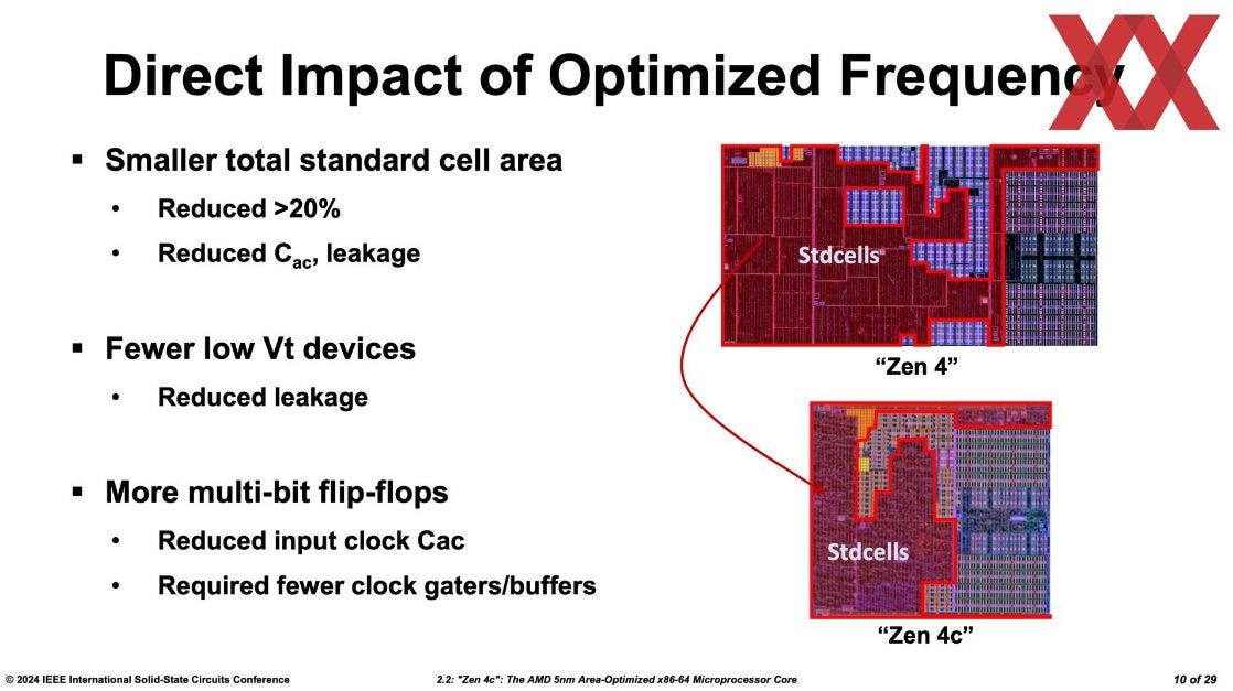
For Zen 4, AMD settled on a different area reduction strategy. Zen 4c leaves the architecture unchanged and targets lower clock speeds to reduce area. Remarkably, even the FPU and its full width 512-bit register file remain unchanged. Limiting Zen 4c to around 3.6 GHz let AMD use denser 6T SRAM for L1 caches, branch prediction storage, and translation caches. A smaller clock mesh and other optimizations let Zen 4c achieve a 35% area reduction for the entire core, not just the FPU. AMD continued by cutting L3 capacity in half, which made a lot of sense because the L3 takes up more area than the cores themselves on server and desktop Zen 2 compute dies (CCDs).
As a result, AMD was able to pack 16 cores into a die that’s just slightly larger than the standard 8 core Zen 4 CCD. That kind of change can open up new market segments, unlike shrinking Zen 2’s FPU in isolation.
We’d like to thank Brutus for dealing with the BC-250.
If you like our articles and journalism, and you want to support us in our endeavors, then consider heading over to our Patreon or our PayPal if you want to toss a few bucks our way. If you would like to talk with the Chips and Cheese staff and the people behind the scenes, then consider joining our Discord.






What surprised me was the CPU memory bandwidth: the APU should be using the same GDDR6 memory (unique on a CPU) with roughly 350 GB/s of bandwidth, yet I measured only about 30 GB/s, which is worse than a DDR4-based system. What could be the reason?
So we are thinking (my team and I) of buying some of these for use on BOINC. BOINC is a distributed computing software that does "science" research for different projects. Most of these projects are CPU based. Anyway you'd be willing to run some tests on some of these projects for us?