Testing AMD’s Giant MI300X
Editor Note (6/26/2024): We have rephrased the acknowledgment section to make more clear that we got no direct support from AMD on this article. Our testing is fully independent, and AMD did not have any involvement during our tests. However, since our expertise is limited in the area of Machine Learning, we reached out to AMD to verify that our numbers are reproducible. This was our only communication with AMD in relation to this article.
AMD’s Radeon Instinct MI300X is the latest in the company’s compute focused CDNA line. NVIDIA has dominated the GPU compute market for time immemorial, thanks to a combination of strong compute GPUs and a dominant software ecosystem (CUDA) that isn’t compatible with competing GPUs. AMD has been trying to strengthen their software side with ROCm, but their first two CDNA generations simply weren’t big enough to challenge NVIDIA’s A100 or H100. With MI300X, AMD is building the biggest, baddest GPU they can to challenge NVIDIA on the hardware front too.
We previously covered the CDNA 3 architecture as presented by AMD. In short, MI300X uses a massive chiplet setup. Eight compute dies, each with 38 CDNA 3 compute units and 4 MB of L2, sit on top of a 256 MB Infinity Cache. All that gets fed with eight HBM3 stacks, providing 5.3 TB/s of bandwidth and 192 GB of DRAM capacity.
Please note that all of our H100 data, except for the inference throughput data, was generated using the PCIe version of H100, which features slower HBM2e memory, fewer CUDA cores, and a reduced TDP of 350 watts. Our inference throughput data was generated on a H100 SXM5 box which has 3.35TB per second of memory bandwidth (compared to the 2.04TB/s of H100 PCIe), 18 more SMs compared to the PCIe version, as well as having an increased TDP of 700 watts.
Acknowledgements
Before diving into the nitty-gritty data, we would like to thank Jon and Clint from Hot Aisle, who without whom this article would not be possible. We would also like to thank Elio from Eliovp and Nscale who assisted us with optimizing our LLM runs. AMD did not directly assist with any of testing but did make sure that our results were reproducible on other MI300X systems.
Cache and Memory Access
Prior CDNA generations were close relatives of AMD’s GCN architecture, and inherited a relatively simple two-level caching setup. CDNA 3 brings over RDNA 2/3’s Infinity Cache to create a third level of cache. Because the L2 cache only has to insulate the cores from Infinity Cache rather than DRAM, L2 capacity goes down to 4 MB. Overall, CDNA 3 shares a lot of RDNA 2’s design goals when it comes to caching.
Compared to CDNA 2, CDNA 3’s cache setup improves latency across the board. L1 latency improves even though cache capacity increases. MI300X’s L2 cache impressively matches RDNA 2’s for latency, even though RDNA 2 clocks higher. However, RDNA 2 still offers better latency for small test sizes. AMD calls RDNA 2’s first level cache a L0, and that name is fitting in this comparison because its mid-level 128 KB L1 cache offers comparable latency to MI300X’s 32 KB L1.
For larger test sizes, CDNA 3’s Infinity Cache comes into play and gives it a massive advantage over CDNA 2. But measuring Infinity Cache latency isn’t so simple. Both MI210 and MI300X see a latency increase at 64 MB, indicating possible address translation penalties.
Like CPUs, GPUs use virtual memory to let multiple processes run concurrently without fear of buggy code in one process corrupting memory used by another. They also use Translation Lookaside Buffers (TLBs) to cache address translations because traversing paging structures with every memory access would be dumb. Missing the TLB increases memory latency as seen by software. MI300X indeed seems to suffer this around the 64 MB mark, because testing with a 4 KB pointer chasing stride shows a clear jump there.

An MI300X XCD appears to be able to store 16384 entries in its TLB, considering that MI300X uses 4K pages and we see a latency jump at 64MB. The latency jumps for L1 and L2 spill out at much higher capacities while the jump at 64 MB didn’t go anywhere, indicating the hardware is tracking data at different granularity. Caches track data with relatively small cache lines (128 bytes on CDNA 3), while TLBs cache translations at the page granularity (4KB on CDNA3). A TLB miss on CDNA 3 appears to have a 47.1 ns penalty, which could come from accessing a second level TLB or going for a page walk.
GPUs usually have multiple TLB instances, so we can increase TLB coverage by dividing the pointer chasing array between multiple workgroups. Now, we can see MI300X’s full 256 MB Infinity Cache from a latency test, alongside 32 MB of total L3 capacity. Infinity Cache latency is around 218 ns. It’s higher latency than RDNA 2’s Infinity Cache, but much better than accessing VRAM.
NVIDIA’s H100 and AMD’s MI300X trade blows depending on test size. H100 has a fast and large L1 cache with 256 KB of capacity, though actual capacity usable as cache can vary because the same storage gets used for software managed local memory. MI300X’s L2 cache offers lower latency, but is much smaller than H100’s. But H100’s L2 is split into two 25 MB halves, and latency increases to the “far” half is worse than Infinity Cache latency on MI300X. MI300X arranges the Infinity Cache across four IO dies, so data coming from the cache has to traverse multiple die boundaries. H100 in contrast is a monolithic design, so Infinity Cache managing to achieve lower latency than H100’s far L2 partition is pretty impressive.
H100 has slightly faster VRAM access from a single thread’s point of view, though at least part of that is likely due to TLB misses on MI300X. If TLB misses are reduced by splitting the array across multiple workgroups, VRAM latency is comparable to H100’s.
Bandwidth
GPUs emphasize high bandwidth because they’re meant for extremely parallel tasks. MI300X’s L1 caches provide massive bandwidth across the GPU, easily outpacing NVIDIA’s H100 PCIe. In an absolute sense, the numbers are pretty ridiculous too. We’re talking about tens of terabytes per second.
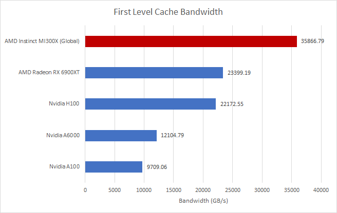
L2 bandwidth is excellent too. MI300X has a 4 MB L2 instance on each compute die, so L2 accesses don’t have to cross die boundaries. Bandwidth from the eight L2 instances adds up to provide crazy bandwidth. In fact, MI300X’s L2 bandwidth lands in the same ballpark as first level cache bandwidth on H100 PCIe.

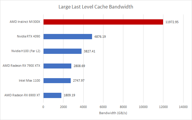
After L2, a lot of recent GPUs use a very large last level cache to maintain high performance without relying too much on memory technology. How GPU makers pull this off varies. NVIDIA and Intel opted to expand L2 capacity, while AMD adds an extra level of cache. For convenience I’ll call this strategy “large last level caching”.
MI300X has the biggest baddest last level cache around, with 256 MB of capacity and more bandwidth than many GPUs have from their L2. Measured figures are a bit off the 17 TB/s theoretical figure, but even 11.9 TB/s is ahead by ridiculous margins. Against NVIDIA’s H100 PCIe, MI300X has more than four times as much cache capacity and a 3x bandwidth lead.
For workloads that don’t play nice with cache, MI300X still overmatches H100 PCIe but not by the same margin. It only has a 2.6x lead in measured bandwidth.

For these tests, we were only able to access a H100 PCIe card from Lambda Cloud. The SXM version of H100 comes with HBM3 and 3.3 TB/s of theoretical bandwidth, and should get a bit closer to MI300X.
Local Memory
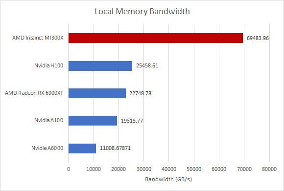
Besides the global memory space backed by VRAM, GPUs have a local memory space backed by small on-die memories. Unlike a cache, software has to explicitly move data into local memory to take advantage of it. But if they can manage it, local memory provides guaranteed low latency and high bandwidth access to that data. MI300X implements local memory with a 64 KB Local Data Share on each Compute Unit, much like prior GCN-based designs. On H100, each SM has a 256 KB block of memory that’s split between L1 cache and local memory, which NVIDIA calls Shared Memory. Up to 224 KB of that block can be allocated as local memory.
MI300X’s local memory bandwidth beats everything else I tested, again including H100. It’s also fun to see how close a consumer graphics oriented GPU like the RX 6900 XT can get to NVIDIA’s H100 in this test.
Besides offering guaranteed high bandwidth, software can expect low latency access to data stored in local memory. With a pointer chasing pattern, MI300X shows a notable improvement over MI210. However, it’s still not a match for consumer cards like the RX 6900 XT. NVIDIA’s H100 offers even better latency to local memory.
Another way to test latency is bouncing a value between two threads through local memory, creating a limited core to core latency test of sorts. Both threads have to share the same block of local memory, which means they’re running on the same MI300X Compute Unit or H100 Streaming Multiprocessor.
MI300X again improves over MI210. NVIDIA GPUs take a heavier latency penalty from handling contended atomics compared to simple reads from a single thread. H100 falls behind MI300X, if only by a hair. The RX 6900 XT leads the pack here, with its higher clock speed and RDNA 2 architecture playing a role.
Global Memory Atomics
Local memory atomics offer speed, but come with a lot of restrictions on which threads can exchange data. Atomics on global memory, which is backed by VRAM, allow data movement and synchronization between any pair of threads.
MI300X has varying performance with global memory atomics, likely depending on where the threads are located on the GPU. Unfortunately I can’t run an all-to-all core to core latency test as with a CPU, because GPU hardware manages where threads get placed. Threads can’t ask to be pinned onto a specific core. However, I can launch one workgroup per CU, and test pairs of workgroups against each other.
Latency ranges from about 116 ns to 202.5 ns depending on which pair of workgroups are exchanging data. Values towards the high end likely correspond to workgroups located on different XCDs, and vice versa for lower latency values. This variability shows the difficulty of constructing such a massive GPU. Just like CPUs, giant GPUs need complex multi-level cache coherency mechanisms.
Compute Throughput
Last time we looked at CDNA 2 in AMD’s MI210, which generally fell short of NVIDIA’s H100 PCIe. MI210 could get close with packed operations, but even then it couldn’t take a lead. H100 was simply a much larger GPU. MI300X flips that around. It’s much larger than H100, and offers a lot more compute throughput. Packed operations, as with INT16, can extend MI300X’s lead even further.
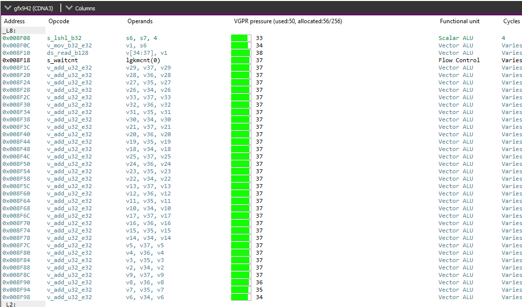
My INT32 add test also behaves as if MI300X is packing values and performing math at double rate, but something definitely went wrong because I don’t think MI300X has that capability. Saving the compiled OpenCL programs and disassembling them shows the compiler is emitting plain INT32 adds.
Contrast that with INT16 adds, which do benefit from packed, double rate execution:
But even disregarding that INT32 result, MI300X on a different planet compared to H100 PCIe. H100 does close the gap somewhat with FP16, but H100 has problems there too. NVIDIA doesn’t advertise support for FP16 through OpenCL, so I’m testing on H100 by not doing the check and using the half datatype anyway.
Special function operations like inverse square roots continue to execute at 4 operations per SIMD cycle, just as on GCN. Those operations are likely less important.
Link Bandwidth
Here, I’m measuring how fast I can copy data between CPU and GPU memory. MI300X benefits from a PCIe Gen 5 x16 interface, and clobbers the competition. NVIDIA’s H100 should support PCIe Gen 5 too, but I wasn’t able to get anywhere near as much bandwidth.

The test system from Hot Aisle had two AMD Epyc 9754 CPUs, each with four MI300X GPUs attached to it. Impressively, I could get the same bandwidth when copying data between a CPU and a GPU that wasn’t directly attached.
However, transferring data to a GPU attached to a remote socket does reduce throughput for low copy sizes. That’s probably because latency tends to dominate with small transfers. With larger transfers, the GPU’s DMA engine can queue up enough requests to hide latency.
Some Light Benchmarking
FluidX3D
FluidX3D uses the lattice Boltzmann method to simulate fluid behavior. It features special optimizations that let it use FP32 and still deliver accurate results in “all but extreme edge cases”. I’m using FluidX3D’s built in benchmark.
With more of everything, MI300X posts a 1.86x performance lead over NVIDIA’s H100 PCIe. FluidX3D can also be compiled to use FP16 for storage. Computations are still performed after converting FP16 values to FP32, so the FP16 modes are mainly there to alleviate memory bandwidth bottlenecks. In exchange, extra math operations for data type conversion tend to increase compute pressure. FP16S uses the standard IEEE FP16 format, while FP16C is a custom FP16 format that needs even more compute for conversion in exchange for better accuracy.
The FP16 storage modes extend MI300X’s lead, as the bottleneck moves from VRAM bandwidth to compute throughput. MI300X’s lead increases slightly to 1.92x with FP16S. With FP16C, MI300X is 2.35x faster than H100 PCIe.
Compute Gravitational Potential
CGP is a self-penned test based on a high school internship project. It takes a map of column density and does a brute-force gravitational potential calculation, which could be used to identify “clumps” with star forming potential. Gravitational forces are very small across large distances, so FP64 is used to handle them. I spent about a day writing this and did not put effort into optimization. The code should be considered representative of what happens if you throw a cup of coffee at a high school intern and tell them to get cracking. To benchmark, I used a 2360×2550 image of the Polaris flare from the Herschel Space Observatory’s SPIRE instrument.
With the quad core Nehalem-based machine I had access to during that internship, generating those results with multithreaded CPU code took a whole weekend. Using OpenCL on MI300X, I can get the results today in 18.2 seconds.
NVIDIA’s H100 PCIe also did a decent job, finishing in just over 54 seconds. However, MI300X is nearly 3x faster, and I know which GPU I would rather use if my high school self could travel forward in time. The Raphael iGPU included with AMD’s Zen 4 desktop CPUs is another option. It can do the same work in 4.2 hours, which leaves time for a coffee break.
This workload could be a best case for MI300X because its memory footprint is just 92 MB. Both the input image and result can fit entirely in MI300X’s Infinity Cache.
Power and thermal limits however leave some performance on the table, and MI300X can’t reach its maximum boost clock of 2.1 GHz. In fairness, NVIDIA’s H100 PCIe also can’t run this workload at maximum clocks because of power and thermal limits. FP64 compute just seems to be very power hungry.
Machine Learning Inference
Machine learning has received a lot of attention lately, especially with large language models that can tell people how to make pizzas with non-toxic glue. With vLLM, and Mistral’s 7.3 billion parameter model, MI300X offers about 16% better inference latency than NVIDIA’s H100 PCIe. Against older GPUs like A100, MI300X has an even larger lead.
These results are consistent with AMD’s slides, which showcase MI300X’s latency advantage over H100 PCIe. AMD tested with Llama, but it’s a good sign that Mistral also enjoys a latency advantage.
An LLM generates tokens one at a time; the full set of model weights, plus the context, has to be read in from VRAM for each new token generated. Taking LLaMA 3 70B as an example, in float16 the weights are approximately 140GB, and the generation context adds another ~2GB. MI300X’s theoretical maximum is 5.3TB/second, which gives us a hard upper limit of (5300 / 142) = ~37.2 tokens per second.

These computations are dominated by Multi-Head Attention, an algorithm that assesses relationships between each token and (as implemented in the majority of LLMs) all the tokens that came before it in the sequence. For a given input sequence, e.g. “What is a road? A road”, the results of those calculations will always be the same.
If we run that sequence through the model and it generates an “is” token, to generate the next token we need to run the entire new “What is a road? A road is” sequence through the model again from the top. This is a lot of redundant computation – we already calculated the values for most of this sequence last time! This is where flash-attention optimization comes in. With flash-attention you can reduce the number of times that you have to go out to memory so you can get much better performance.

But we can improve performance even more with KV caching. With KV caching, we save the result of the Attention calculations for the previous sequence in HBM. When the new sequence is processed, rather than recomputing Attention values for the entire sequence, we load the cached result from “What is a road? A road” and pick up the calculations where they were left off – as if the sequence had been “What is a road? A road is” right from the start. The cached KV values are typically only a few GB, vastly reducing the required bandwidth per token.
Starting with Mixtral 8-7B inference performance, MI300X puts up a very good showing. Looking at the difference between KVcache enabled and disabled, there is a nearly 34x increase in the tokens per second. Then compared to GH200, at the same input and output length of 128, we see that MI300X ends up about 10% ahead. Comparing to 2 H100 SXM5 GPUs, at the same input and output length of 2048, a single MI300X ends up around 70% the performance. It’s fairly impressive when you consider that it’s two H100 SXM5s versus one MI300X.
Turning to LLaMA3-70B, MI300X wins by default here. A single H100 SXM5 with 80GB of HBM3 cannot run LLaMA3-70B while using FP16, and 2 H100 SXM5s cannot match the performance of a single MI300X. Looking at the H100 SXM5 INT8 result, it is likely that even at INT8 H100 SXM5 is running out of memory for KVcache so it is likely not caching tokens.
Final Words: Attacking NVIDIA’s Hardware Dominance
AMD has been a second place player for a long time. Their GPUs can rarely compete in the same market segment as NVIDIA’s. When they do, NVIDIA is able to win on features. Terascale 2 provided competitive performance at lower power in 2009, but NVIDIA’s Fermi handled better with extreme tessellation factors. More than a decade later, AMD’s RX 6900 XT could go head to head with NVIDIA’s Ampere, but lost when raytracing was thrown into the mix. At other times, NVIDIA’s dominance was completely unquestioned, with no AMD GPU in that generation able to fight in the same neighborhood as NVIDIA’s best regardless of add-on features.
The competitive situation is even more dire for compute GPUs. NVIDIA’s CUDA software ecosystem provided pre-optimized libraries and only worked on their GPUs. NVIDIA’s compute GPUs themselves were much larger and more capable than competing AMD options. H100 for example dominated against AMD’s MI210. AMD did build a MI250X with two CDNA 2 dies, but had to expose each die as a separate logical GPU. If you wanted the biggest compute GPU money could buy, it had to come from NVIDIA.
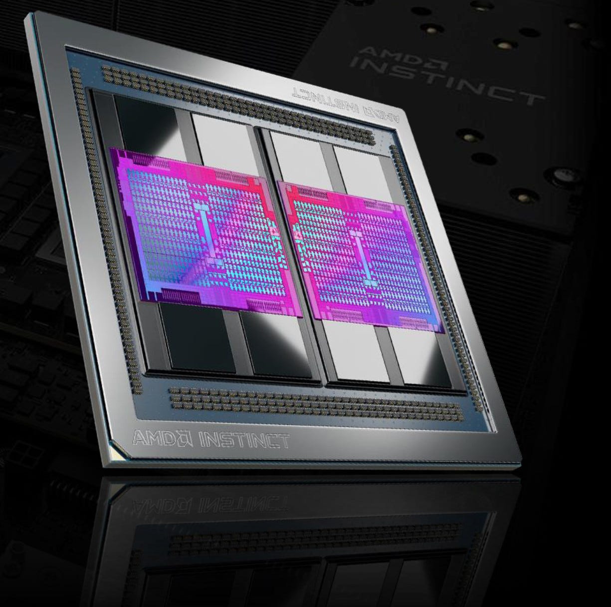
AMD’s Radeon Instinct MI300X changes that. For the first time in the history of compute-focused GPUs, AMD has built a much larger GPU than NVIDIA. To accomplish this, AMD used a very ambitious chiplet setup coupled with techniques brought over from other projects. Infinity Cache was first tested in AMD’s RDNA 2. Vertically stacked cache was tested in Zen 3. Zen 2 debuted a hub-and-spoke chiplet architecture with compute chiplets accessing memory through an IO die. Experience from those less aggressive setups certainly added to AMD’s confidence when they started working on CDNA 3.
MI300X does a lot of new and difficult things too. Instead of one IO die, there are four connected by very high bandwidth links. Compute dies are stacked on top of IO dies, which are stacked on top of an interposer to create a triple level setup. On the architecture side, CDNA 3 is no small iteration over CDNA 2. CDNA 3 Compute Units have tweaked caches, more scheduler entries, more compute throughput, and a new dual issue scheme to feed it. AMD deserves a lot of credit for putting MI300X together without eating half a decade of delays. And it’s refreshing to see AMD shoot for first place.
But we must now talk about the elephant in the room, and that is AMD’s software stack. While it is absolutely night and day from where it was when we tested MI210, ROCm is nowhere near where it needs to be to truly compete with CUDA. Upstream flash-attention still has no real support for CDNA3; there are open PRs with a Triton implementation for FP16 and FP32, but no bfloat16, and HIPifying the existing kernels either doesn’t work or doesn’t take full advantage of the available on-chip cache.
AMD has been working on this, but they are still a long way away from where they need to be. Something that would vastly improve their software stack is if ROCm was universal like CUDA is. With CUDA you can pick up any NVIDIA GPU, from the lowly 50 series of cards shoved into a laptop all the way up to the 90 series of cards, and be confident that CUDA will run on it. This allowed developers to optimize solely for CUDA and its well-optimized libraries. That is not the case with ROCm, you can’t pick up an AMD GPU or APU and be sure that it runs ROCm and all of the associated libraries. At Computex, we had a chance to ask Dr. Lisa Su about widespread ROCm, where she said,
“ROCm on AMD is important. The focus with ROCm has been on Data Center GPU side, and that’s where a lot of effort is, that’s where performance is. We want people to be able to use ROCm on all devices. We’ve started to expand with ROCm on Radeon, and over time we’ll see ROCm on APUs as well.”
Dr. Lisa Su, CEO and President of AMD, Computex 2024 Press Q&A
This is a good sign that AMD will have widespread support across all of AMD’s GPUs and APUs and we hope that this support comes quickly. There have been LLVM commits that show that AMD is going to use SPIR-V as an intermediate representation between ROCm and the assembly language, similar to NVIDIA’s PTX. Hopefully this will allow for widespread ROCm, and all ROCm libraries’, support across all of AMD’s products: from the integrated graphics found on AMD’s CPUs and APU to all of AMD’s Radeon GPUs, along with continuing to improve the ROCm experience on their Datacenter GPUs.
When it is all said and done, MI300X is a very impressive piece of hardware. However, the software side suffers from a chicken-and-egg dilemma. Developers are hesitant to invest in a platform with limited adoption, but the platform also depends on their support. Hopefully the software side of the equation gets into ship shape. Should that happen, AMD would be a serious competitor to NVIDIA.
Again, we would like to thank Jon and Clint from Hot Aisle for access to the system, Elio from Eliovp and Nscale for helping us with optimizing our inference tests, and AMD for making sure our results are reproducible on other systems. If you like our articles and journalism, and you want to support us in our endeavors, then consider heading over to our Patreon or our PayPal if you want to toss a few bucks our way. If you would like to talk with the Chips and Cheese staff and the people behind the scenes, then consider joining our Discord.






Amazing work dudes!
I know its been 2 years... but want to help me do the same for CDNA4 ? I'm trying to build a PP inference engine for DS's V3.2 and just can't do shit with no numbers.
I also really want to profile inter-die latencies with NPS1 vs NPS4
I found a place renting them fully on demand 💪